Digital VLSI Design and Simulation with Verilog
Dr. Suman Lata Tripathi
Lovely Professional University, Phagwara, Punjab, India
Dr. Sobhit Saxena
Lovely Professional University, Phagwara, Punjab, India
Dr. Sanjeet Kumar Sinha
Lovely Professional University, Phagwara, Punjab, India
Dr. Govind Singh Patel
IIMT College of Engineering, Greater Noida, UP, India
This edition first published 2022 © 2022 John Wiley & Sons Ltd.
All rights reserved. No part of this publication may be reproduced, stored in a retrieval system, or transmitted, in any form or by any means, electronic, mechanical, photocopying, recording or otherwise, except as permitted by law. Advice on how to obtain permission to reuse material from this title is available at http://www.wiley.com/go/permissions.
The right of Suman Lata Tripathi, Sobhit Saxena, Sanjeet Kumar Sinha, and Govind Singh Patel to be identified as the authors of this work has been asserted in accordance with law.
Registered Office
John Wiley & Sons, Inc., 111 River Street, Hoboken, NJ 07030, USA
Editorial Office
9600 Garsington Road, Oxford, OX4 2DQ, UK
For details of our global editorial offices, customer services, and more information about Wiley products visit us at www.wiley.com.
Wiley also publishes its books in a variety of electronic formats and by print-on-demand. Some content that appears in standard print versions of this book may not be available in other formats.
Limit of Liability/Disclaimer of Warranty
While the publisher and authors have used their best efforts in preparing this work, they make no representations or warranties with respect to the accuracy or completeness of the contents of this work and specifically disclaim all warranties, including without limitation any implied warranties of merchantability or fitness for a particular purpose. No warranty may be created or extended by sales representatives, written sales materials or promotional statements for this work. The fact that an organization, website, or product is referred to in this work as a citation and/or potential source of further information does not mean that the publisher and authors endorse the information or services the organization, website, or product may provide or recommendations it may make. This work is sold with the understanding that the publisher is not engaged in rendering professional services. The advice and strategies contained herein may not be suitable for your situation. You should consult with a specialist where appropriate. Further, readers should be aware that websites listed in this work may have changed or disappeared between when this work was written and when it is read. Neither the publisher nor authors shall be liable for any loss of profit or any other commercial damages, including but not limited to special, incidental, consequential, or other damages.
Library of Congress Cataloging-in-Publication Data
Names: Tripathi, Suman Lata, author. | Saxena, Sobhit, author. | Sinha, Sanjeet Kumar, author. | Patel, Govind Singh, author.
Title: Digital VLSI design and simulation with Verilog / Suman Lata Tripathi, Sobhit Saxena, Sanjeet Kumar Sinha, Govind Singh Patel.
Description: Hoboken, NJ : John Wiley & Sons, 2022. | Includes bibliographical references and index.
Identifiers: LCCN 2021020790 (print) | LCCN 2021020791 (ebook) | ISBN 9781119778042 (hardback) | ISBN 9781119778066 (pdf) | ISBN 9781119778080 (epub) | ISBN 9781119778097 (ebook)
Subjects: LCSH: Integrated circuits--Very large scale integration--Design and construction. | Verilog (Computer hardware description language)
Classification: LCC TK7874.75 .T75 2022 (print) | LCC TK7874.75 (ebook) | DDC 621.39/5028553--dc23
LC record available at https://lccn.loc.gov/2021020790
LC ebook record available at https://lccn.loc.gov/2021020791
Cover image: © Raigvi/Shutterstock
Cover design by Wiley
Set in 9.5/12.5 STIXTwoText by Integra Software Services Pvt. Ltd, Pondicherry, India
10 9 8 7 6 5 4 3 2 1
Contents
Preface xi
About the Authors xiii
1 Combinational Circuit Design 1
1.1 Logic Gates 1
1.1.1 Universal Gate Operation 3
1.1.2 Combinational Logic Circuits 5
1.2 Combinational Logic Circuits Using MSI 6
1.2.1 Adders 6
1.2.2 Multiplexers 12
1.2.3 De-multiplexer 14
1.2.4 Decoders 15
1.2.5 Multiplier 17
1.2.6 Comparators 18
1.2.7 Code Converters 19
1.2.8 Decimal to BCD Encoder 20
Review Questions 21 Multiple Choice Questions 22 Reference 23
2 Sequential Circuit Design 25
2.1 Flip-flops (F/F) 25
2.1.1 S-R F/F 25
2.1.2 D F/F 26
2.1.3 J-K F/F 26
2.1.4 T F/F 28
2.1.5 F/F Excitation Table 29
2.1.6 F/F Characteristic Table 29
2.2 Registers 31
2.2.1 Serial I/P and Serial O/P (SISO) 31
2.2.2 Serial Input and Parallel Output (SIPO) 31
2.2.3 Parallel Input and Parallel Output (PIPO) 32
2.2.4 Parallel Input and Serial Output (PISO) 32
2.3 Counters 33
2.3.1 Synchronous Counter 33
2.3.2 Asynchronous Counter 33
2.3.3 Design of a 3-Bit Synchronous Up-counter 34
2.3.4 Ring Counter 36
2.3.5 Johnson Counter 37
2.4 Finite State Machine (FSM) 37
2.4.1 Mealy and Moore Machine 38
2.4.2 Pattern or Sequence Detector 38 Review Questions 41 Multiple Choice Questions 41 Reference 42
3 Introduction to Verilog HDL 43
3.1 Basics of Verilog HDL 43
3.1.1 Introduction to VLSI 43
3.1.2 Analog and Digital VLSI 43
3.1.3 Machine Language and HDLs 44
3.1.4 Design Methodologies 44
3.1.5 Design Flow 45
3.2 Level of Abstractions and Modeling Concepts 45
3.2.1 Gate Level 45
3.2.2 Dataflow Level 47
3.2.3 Behavioral Level 47
3.2.4 Switch Level 47
3.3 Basics (Lexical) Conventions 47
3.3.1 Comments 47
3.3.2 Whitespace 48
3.3.3 Identifiers 48
3.3.4 Escaped Identifiers 48
3.3.5 Keywords 48
3.3.6 Strings 49
3.3.7 Operators 49
3.3.8 Numbers 49
3.4 Data Types 50
3.4.1 Values 50
3.4.2 Nets 50
3.4.3 Registers 51
3.4.4 Vectors 51
3.4.5 Integer Data Type 51
3.4.6 Real Data Type 51
3.4.7 Time Data Type 52
3.4.8 Arrays 52
3.4.9 Memories 52
3.5 Testbench Concept 53
Multiple Choice Questions 53 References 54
4 Programming Techniques in Verilog I 55
4.1 Programming Techniques in Verilog I 55
4.2 Gate-Level Model of Circuits 55
4.3 Combinational Circuits 57
4.3.1 Adder and Subtractor 57
4.3.2 Multiplexer and De-multiplexer 66
4.3.3 Decoder and Encoder 71
4.3.4 Comparator 75
Review Questions 77
Multiple Choice Questions 77 References 78
5 Programming Techniques in Verilog II 79
5.1 Programming Techniques in Verilog II 79
5.2 Dataflow Model of Circuits 79
5.3 Dataflow Model of Combinational Circuits 80
5.3.1 Adder and Subtractor 80
5.3.2 Multiplexer 82
5.3.3 Decoder 85
5.3.4 Comparator 86
5.4 Testbench 87
5.4.1 Dataflow Model of the Half Adder and Testbench 88
5.4.2 Dataflow Model of the Half Subtractor and Testbench 89
5.4.3 Dataflow Model of 2 × 1 Mux and Testbench 90
5.4.4 Dataflow Model of 4 × 1 Mux and Testbench 91
5.4.5 Dataflow Model of 2-to-4 Decoder and Testbench 92
Review Questions 93
Multiple Choice Questions 94 References 95
6 Programming Techniques in Verilog II 97
6.1 Programming Techniques in Verilog II 97
6.2 Behavioral Model of Combinational Circuits 98
6.2.1 Behavioral Code of a Half Adder Using If-else 98
6.2.2 Behavioral Code of a Full Adder Using Half Adders 99
6.2.3 Behavioral Code of a 4-bit Full Adder (FA) 100
6.2.4 Behavioral Model of Multiplexer Circuits 101
6.2.5 Behavioral Model of a 2-to-4 Decoder 104
6.2.6 Behavioral Model of a 4-to-2 Encoder 106
6.3 Behavioral Model of Sequential Circuits 108
6.3.1 Behavioral Modeling of the D-Latch 108
6.3.2 Behavioral Modeling of the D-F/F 109
6.3.3 Behavioral Modeling of the J-K F/F 110
6.3.4 Behavioral Modeling of the D-F/F Using J-K F/F 112
6.3.5 Behavioral Modeling of the T-F/F Using J-K F/F 113
6.3.6 Behavior Modeling of an S-R F/F Using J-K F/F 114
Review Questions 115
Multiple Choice Questions 115 References 116
7 Digital Design Using Switches 117
7.1 Switch-Level Model 117
7.2 Digital Design Using CMOS Technology 118
7.3 CMOS Inverter 119
7.4 Design and Implementation of the Combinational Circuit Using Switches 120
7.4.1 Types of Switches 120
7.4.2 CMOS Switches 121
7.4.3 Resistive Switches 121
7.4.4 Bidirectional Switches 122
7.4.5 Supply and Ground Requirements 122
7.5 Logic Implementation Using Switches 123
7.5.1 Digital Design with a Transmission Gate 127
7.6 Implementation with Bidirectional Switches 127
7.6.1 Multiplexer Using Switches 127
7.7 Verilog Switch-Level Description with Structural-Level Modeling 131
7.8 Delay Model with Switches 131 Review Questions 132
Multiple Choice Questions 133 References 134
8 Advance Verilog Topics 135
8.1 Delay Modeling and Programming 135
8.1.1 Delay Modeling 135
8.1.2 Distributed-Delay Model 135
8.1.3 Lumped-Delay Model 136
8.1.4 Pin-to-Pin-Delay Model 137
8.2 User-Defined Primitive (UDP) 138
8.2.1 Combinational UDPs 139
8.2.2 Sequential UDPs 142
8.2.3 Shorthands in UDP 144
8.3 Task and Function 144
8.3.1 Difference between Task and Function 144
8.3.2 Syntax of Task and Function Declaration 145
8.3.3 Invoking Task and Function 147
8.3.4 Examples of Task Declaration and Invocation 147
8.3.5 Examples of Function Declaration and Invocation 148 Review Questions 148
Multiple Choice Questions 149 References 149
9 Programmable and Reconfigurable Devices 151
9.1 Logic Synthesis 151
9.1.1 Technology Mapping 151
9.1.2 Technology Libraries 152
9.2 Introduction of a Programmable Logic Device 152
9.2.1 PROM, PAL and PLA 153
9.2.2 SPLD and CPLD 154
9.3 Field-Programmable Gate Array 156
9.3.1 FPGA Architecture 158
9.4 Shannon’s Expansion and Look-up Table 158
9.4.1 2-Input LUT 159
9.4.2 3-Input LUT 160
9.5 FPGA Families 161
9.6 Programming with FPGA 161
9.6.1 Introduction to Xilinx Vivado Design Suite for FPGA-Based Implementations 163
9.7 ASIC and Its Applications 163 Review Questions 164
Multiple Choice Questions 164 References 167
10 Project Based on Verilog HDLs 169
10.1 Project Based on Combinational Circuit Design Using Verilog HDL 171
10.1.1 Full Adder Using Switches at Structural Level Model 171
10.1.2 Ripple-Carry Full Adder (RCFA) 174
10.1.3 4-bit Carry Look-ahead Adder (CLA) 174
10.1.4 Design of a 4-bit Carry Save Adder (CSA) 176
10.1.5 2-bit Array Multiplier 177
10.1.6 2 × 2 Bit Division Circuit Design 178
10.1.7 2-bit Comparator 179
10.1.8 16-bit Arithmetic Logic Unit 180
10.1.9 Design and Implementation of 4 × 16 Decoder Using 2 × 4 Decoder 181
10.2 Project Based on Sequential Circuit Design Using Verilog HDL 182
10.2.1 Design of 4-bit Up/down Counter 182
10.2.2 LFSR Based 8-bit Test Pattern Generator 183
10.3 Counter Design 185
10.3.1 Random Counter that Counts Sequence like 2,4,6,8,2,8…and so On 185
10.3.2 Use of Task at the Behavioral-Level Model 187
10.3.3 Traffic Signal Light Controller 188
10.3.4 Hamming Code(h,k) Encoder/Decoder 189 Review Questions 192 Multiple Choice Questions 192 References 193
11 SystemVerilog 195
11.1 Introduction 195
11.2 Distinct Features of SystemVerilog 195
11.2.1 Data Types 196
11.2.2 Arrays 197
11.2.3 Typedef 199
11.2.4 Enum 200
11.3 Always_type 201
11.4 $log2c() Function 202
11.5 System-Verilog as a Verification Language 203 Review Questions 203
Multiple Choice Questions 204 Reference 204
Index 205
Preface
Integrated circuits are now growing in importance in every electronic system that needs an efficient VLSI architecture design with low-power consumption, a compress chip area, speed, and operating frequency. The challenge for VLSI system designers is to optimize hardware-software integration for lowering the total cost of product acquisition. So, there is a demand for better technological solutions for advanced VLSI architectures that can be done through hardware description language (HDL). Verilog HDL is one of the programming languages that can provide better solutions in this new era of the VLSI industry. The prefabrication design and analysis of such advanced VLSI architecture can easily be implemented with Verilog HDL using available software tools such as Xilinx and Cadence.
This book mainly deals with the fundamental concepts of digital design along with their design verification with Verilog HDL. It will be a common source of knowledge for beginners as well as research-seeking students working in the area of VLSI design, covering fundamentals of digital design from switch level to FPGA-based implementation using hardware description language (HDL).
The book is summarized in 10 chapters. Chapters 1 and 2 describe the fundamental concepts behind digital circuit design including combinational and sequential circuit design. Chapters 3 to 8 focus on sequential and combinational circuit design using Verilog HDL at different levels of abstraction in Verilog coding. Chapter 9 includes implementation of any logic function using a programmable logic device such as PLD, CPLD, FPGA, etc. Chapter 10 covers a few real-time examples of digital circuit design using Verilog. Chapter 11 focuses on System Verilog, distinct features, computing Verilog and System Verilog with design example.
About the Authors
Dr. Suman Lata Tripathi completed her PhD in the area of microelectronics and VLSI from Motilal Nehru National Institute of Technology, Allahabad. She obtained her M.Tech in Electronics Engineering from Uttar Pradesh Technical University, Lucknow and B.Tech in Electrical Engineering from Purvanchal University, Jaunpur. She is associated with Lovely Professional University as a Professor with more than 17 years of experience in academics. She has published more than 55 research papers in refereed IEEE, Springer, and IOP science journals and conferences. She has organized several workshops, summer internships, and expert lectures for students. She has worked as a session chair, conference steering committee member, editorial board member, and reviewer in international/national IEEE/Springer Journal and conferences. She received the “Research Excellence Award” in 2019 at Lovely Professional University. She received the best paper at IEEE ICICS-2018. She has edited more than 12 books/1 book series in different areas of electronics and electrical engineering. She is associated with editing work for top publishers including Elsevier, CRC, Taylor and Francis, Wiley-IEEE, SP Wiley, Nova Science, and Apple Academic Press. She also works as series editor for, “Smart Engineering Systems” CRC Press, Taylor and Francis. She is associated as a senior member IEEE, Fellow IETE and Life member of ISC and is continuously involved in different professional activities along with her academic work. Her area of expertise includes microelectronics device modeling and characterization, low-power VLSI circuit design, VLSI design of testing, and advance FET design for IoT, Embedded System Design and biomedical applications etc.
Dr. Sobhit Saxena completed his PhD at “IIT Roorkee” from the Metallurgical & Materials Engineering Department. He has designed a new hybrid system of Li-ion battery and supercapacitor for energy storage applications. He worked as SEM (Scanning Electron Microscopy) operator for 4 years under the MHRD fellowship. He obtained his M.Tech in VLSI from Shobhit University, Meerut
and B.E. from MIT Moradabad in Electronics and Communication Engineering. He has vast teaching experience of more than 10 years in various colleges and universities. Currently, he is working as Associate Professor in the School of Electronics and Electrical Engineering, Lovely Professional University. He has been awarded the “Perfect Award” four times consecutively (2007–2010) for achieving 100% results. He has published around 12 research papers in SCIindexed journals and reputed international conferences held at different IITs. His area of expertise includes nanomaterial synthesis and characterization, electrochemical analysis and modeling and simulation of CNT based interconnects for VLSI circuits.
Dr. Sanjeet Kumar Sinha completed a doctoral program in the Department of Electrical Engineering of the National Institute of Technology (NIT) Silchar. He obtained his M.Tech in Microelectronics and VLSI Design from NIT Silchar. He is associated with Lovely Professional University as an Associate Professor with more than 10 years of experience in academia. Over the years, he has developed an innovative approach to teaching and conducting research with undergraduates through creating and presenting course materials in both laboratory and classroom settings. He has published around 35 research papers in refereed journals/conferences including Elsevier, IEEE transaction, etc. He has published book chapters in Elsevier, Taylor & Francis, etc. His area of expertise includes microelectronics device modeling and characterization, low-power VLSI circuit design, VLSI design of testing, fabrication & characterization of CNT FET, etc.
Dr. Govind Singh Patel received his Masters degree in Instrumentation & Control Engineering from MD University, Rohtak, India. He has studied and been awarded a PhD in Electronics and Communication Engineering from Thapar University, Patiala, India. He is working as Professor in the Department of Electronics and Communication Engineering, IIMT Engineering College, Greater Noida, UP, India. He has published more than 62 papers in National and International Journals. He has also filed four Indian patents. His area of expertise includes VLSI signal processing, communication systems, low-power VLSI circuit design, VLSI design &testing and advance electronics, design for IoT, and agriculture applications. His one book titled “Smart Agriculture: Deep Learning, Machine Learning and IoT” is in the process of publication with CRC Taylor and Francis.
Combinational Circuit Design
This chapter describes the combinational logic circuits design and their implementation with logic gates, multiplexers, decoders, etc. Combinational circuits are the major block of any digital design or function [1]. So, a detailed overview before the design and analysis of digital circuit with Verilog modules, plays a significant role in hardware optimization to achieve the desired outcomes.
1.1 Logic Gates
Logic gates are very useful when performing a few basic operations in any digital computer system. These logic gates perform many operations in complex circuits and other control systems, e.g., basic operations like AND, OR, and NOT. The functionality of each basic gate as well as the extended version are discussed in this chapter.
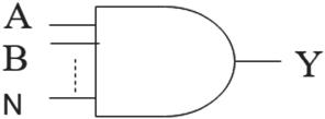
AND operation:
It performs the AND operation. The circuit diagram of the N input AND operation is shown in Figure 1.1.
Figure 1.1 Symbol of an AND gate.
Digital VLSI Design and Simulation with Verilog, First Edition. Suman Lata Tripathi, Sobhit Saxena, Sanjeet Kumar Sinha, and Govind Singh Patel. © 2022 John Wiley & Sons Ltd. Published 2022 by John Wiley & Sons Ltd.
Combinational Circuit Design 2
The AND gate may have N number of inputs and one output. If the number of inputs are N then N ≥ 2 conditions must be applied for input operation. Digital inputs are applied in terms of A, B, C……N, and the output is Y.
The mathematic equation is given below:
Y= A ANDB ANDC ANDD ANDN = A.B.C.DN = ABCD N ……… …… . . .
The truth table for an AND gate is provided in Table 1.1
Table 1.1 T. Table of AND gate.
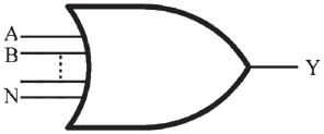
OR operation: It performs OR operation. The symbol for an OR operation is shown in Figure 1.2.
Figure 1.2 Symbol for an OR gate.
The OR gate may have N number of inputs and one output. If the number of inputs are N then N ≥ 2 conditions must be applied for input operation. Digital inputs are applied in terms of A, B, C……N, and the output is Y.
The mathematic equation is given below:
Y = AORB OR CORD ORN = A+B+C+D+ N .
The truth table for an OR gate is provided in Table 1.2.
Table 1.2 Truth table of an OR gate.
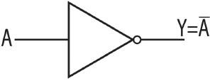
NOT operation:
This is also called an inverter. The symbol for the NOT gate is shown in Figure 1.3. It has a single input device and it generates an inverted output. Table 1.3 describes the truth table of a NOT gate. The mathematical equation is written as: Y = NOTA = A
Figure 1.3 Symbol for a NOT gate.
Table 1.3 Truth table of a NOT gate.
1.1.1 Universal Gate Operation
Universal gates are those in which any logical expression can be realized. The NAND and NOR gates are very popular and are widely used for realization of logical expressions. Therefore, these two NAND and NOR gates are used to implement other gates so these are called universal gates.
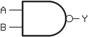
NAND operation
This is a universal gate. The operation NOT-AND is known as a NAND operation. It has N number of inputs and one output like other basic gates. However, two inputs and one output NAND gate are shown in Figure 1.4. Table 1.4 provides output values of a NAND gate in terms of inputs. The Boolean equation is given below: Y AB =
Figure 1.4 Symbol for a NAND gate.
Table 1.4 Truth table of a NAND gate.
NOR operation
This is a universal gate. The operation NOT-OR is known as a NOR operation. It has N number of inputs and one output similar to basic gates. The symbol diagram of two inputs and one output is shown in Figure 1.5. Table 1.5 gives output values of a NOR gate in terms of inputs. The Boolean equation is given below: Y AB =+
Figure 1.5 Symbol for a NOR gate.
Table 1.5 Truth table of a NOR gate.
EX-OR Operation
The operation EX-OR is used in many applications. It has N number of inputs and one output like other basic gates. The symbol diagram of two I/P and one O/P is shown in Figure 1.6. Table 1.6 provides the output values of an EX-OR gate in terms of inputs. Its mathematic equation is given below:
Y AB =⊕
Figure 1.6 Symbol for a NAND gate.
Table 1.6 Truth table of a NAND gate.
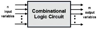
1.1.2 Combinational Logic Circuits
This type of circuit depends upon the I/Ps in that particular instant of time. A memory element is not available. A combinational circuit may have a number of sub-systems as shown in Figure 1.7.
There are many ways to design these combinational logic circuits. These include:
1. Boolean expression
2. Set of statement
3. Truth table
These designs are used to design combinational logic circuits. However, a number of methods are also available to simplify Boolean function. These include:
a) Algebraic method
b) K-map method
c) Variable entered method
d) Tabulation method
Standard representation for logical functions
Any logical functions can be represented in terms of their logical variables. Logical variables and their functions are in binary form. There are two standard forms generally being used in circuit designing.
1. Sum of product (SOP)
2. Product of sum (POS)
Apart from the form above, other forms are also available to design circuits. However, these forms are conveniently suitable for the design process. This is discussed in more detail in the next subsection.
1.2 Combinational Logic Circuits Using MSI
This subsection describes the simplification and realization of the combinational logic circuits using gates. These methods are used to integrate complex functions in the form of IC. There are many devices are available such as adders, multiplexers, de-multiplexers, decoders, and multipliers.
1.2.1 Adders
An adder is a combinational logic circuit that performs arithmetic sums of binary numbers and produces corresponding outputs.
Figure 1.7 Diagram of a combinational logic circuit.
1.2 Combinational Logic Circuits Using MSI 7
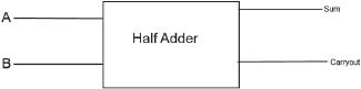
Half Adder
This is a basic adder that performs arithmetic sums of two inputs and gives the corresponding output in terms of sum and carry. The diagram of a H. adder is shown in Figure 1.8.
Figure 1.8 Block diagram of a H. adder.
A and B are I/Ps and O/Ps and are the sum and carry of the H. adder. The truth table is given in Table 1.7.
Table 1.7 Truth table of a half adder.
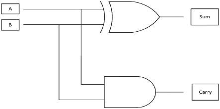
Mathematical expressions for the H. adder are:
SumABAB Carry AB =+ =⊕ = AB
The circuit diagram of the H. adder is shown in Figure 1.9.
Figure 1.9 Circuit diagram of a half adder.
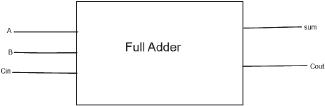
Full Adder
This performs the arithmetic sum of three inputs and gives the corresponding two outputs in terms of sum and carry. A block diagram of the full adder is shown in Figure 1.10. Table 1.8 provides the truth table of a full adder circuit where output variables (Sum, Cout) are expressed in terms of input values.
Figure 1.10 Block diagram of a full adder.
Table 1.8 Truth table of a full adder.
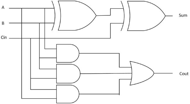
Boolean expressions for the F. adder are: K-Map for Sum:
K-Map for Cout:
Combinational Logic Circuits
Logic diagram of a full adder
A logical representation of the F. adder is shown in Figure 1.11.
Figure 1.11 Full adder logic block.
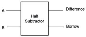
Half Subtractor
A half subtractor is a combinational logic circuit that performs the arithmetic difference between two inputs and provides the corresponding output in terms of difference and borrows as shown in Figure 1.12. Table 1.9 provides output variables (Difference, Borrow) of the half subtractor in terms of inputs (A,B).
Figure 1.12 Half subtractor.
Table 1.9 Truth table of the H. subtractor.
B Difference Borrow
1 Combinational Circuit Design 10
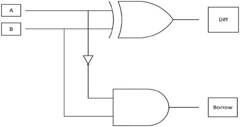
Boolean expressions for the H. adder are:
Diff = AB+AB = AB
Borrow = AB ⊕
Logic diagram of a H. Subtractor
The logical representation of a H. adder is shown in Figure 1.13.
Figure 1.13 Half subtractor logic block.
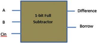
Full Subtractor
This performs the arithmetic difference of three inputs and gives corresponding two outputs in terms of Diff. and Borrow. A block diagram of the F. subtractor is shown in Figure 1.14. Table 1.10 provides output variables (Difference, Borrow) of the full subtractor in terms of inputs (A,B).
Figure 1.14 Block diagram of the full subtractor.
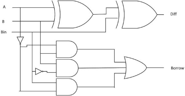
K-Map for Difference:
Table 1.10 Truth table of the full subtractor.
1.2 Combinational Logic Circuits Using MSI 11
A mathematical equation for the F. subtractor is:
Diff AB Bin =⊕ ⊕
K-Map for Borrow: B’Bin’ B’Bin BBin BBin’
BorrowABABBB in in =+ +
The logic diagram of the F. subtractor is shown in Figure 1.15.
Figure 1.15 Full subtractor logic block.
1.2.2 Multiplexers
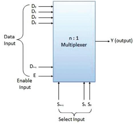
This is a type of combinational circuit. It has multiple inputs and a single output and its output depends upon the select lines. Select lines control the processing of the multiplexer which means that whatever the input is will be the output depending on select lines. If N select lines then input lines will be 2 N as shown in Figure 1.16.
Figure 1.16 Block diagram of the multiplexer.
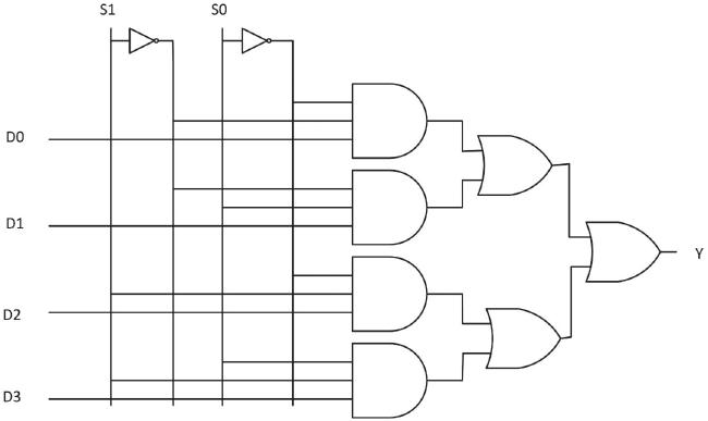
For simplicity of the expression, 4:1 MUX has been explained in the truth table. The truth table for 4:1 MUX is given in Table 1.11.
Table 1.11 Truth table of the 4:1 MUX.
The Boolean expression for Y can be expressed as:
++ 10 01 01 10 21 03
The logic diagram of a multiplexer is shown in Figure 1.17.
1.2 Combinational Logic Circuits Using
1.17 Logic diagram of the multiplexer.
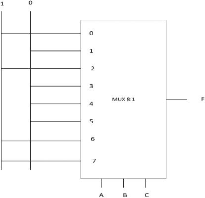
Example:
Implement the expression FA BC m ,, ,,, () = () ∑ 0 267 using a multiplexer.
Solution:
There are four variables; therefore, it needs four select lines for the process. And there are four Minterms which means these inputs are connected with logic 1 and the remaining with logic 0. For this implementation, 8:1 MUX is required. The implementation is shown in Figure 1.18.
Figure 1.18 Implementation of function.
Figure
Advantages of multiplexers:
1. Logic circuits can be implemented without simplification of the logic expression.
2. This reduces the integrated circuit count.
3. Logic design can be simplified.
1.2.3 De-multiplexer
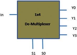
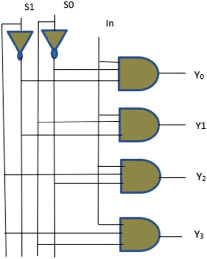
A de-multiplexer provides 2N outputs for N select lines and a single input. These controls are used to select which O/P line to route the I/P. For example, a 1 × 4 de-multiplexer has one input and four output lines for two select or control lines, as shown in Figure 1.19. Table 1.12 describes the truth table of the de-multiplexer shown in Figure 1.19.
1.19 Block diagram of the de-multiplexer.
Table 1.12 Truth table of a 1 × 4 de-multiplexer.
With the help of the truth table, the de-multiplexer output can be expressed as:
A logical representation of the de-multiplexer is shown in Figure 1.20.
Figure
Figure 1.20 1 × 4 de-multiplexer using logic gates.
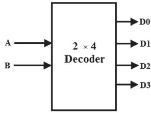
1.2.4 Decoders
This is a type of combinational circuit used to decode binary data. There are several decoders such as the BCD to seven-segment decoder, Decimal to BCD decoder etc. Here, the basic decoder 2:4 is being discussed, as shown in Figure 1.21. Table 1.13 shows the truth table of a 2:4 line decoder.
Figure 1.21 Block diagram of a 2 × 4 decoder.