
Photovoltaic module reliability Wohlgemuth
Visit to download the full and correct content document: https://ebookmass.com/product/photovoltaic-module-reliability-wohlgemuth/

More products digital (pdf, epub, mobi) instant download maybe you interests ...

Advances in system reliability engineering Davim
https://ebookmass.com/product/advances-in-system-reliabilityengineering-davim/
Safety and Reliability Modeling and Its Applications (Advances in Reliability Science) 1st Edition Mangey Ram (Editor)
https://ebookmass.com/product/safety-and-reliability-modelingand-its-applications-advances-in-reliability-science-1st-editionmangey-ram-editor/

Engineering Reliability and Risk Assessment Harish Garg
https://ebookmass.com/product/engineering-reliability-and-riskassessment-harish-garg/
Practical Reliability Engineering 5th Edition – Ebook PDF Version
https://ebookmass.com/product/practical-reliabilityengineering-5th-edition-ebook-pdf-version/

Introduction to Reliability Engineering 3rd Edition
James E. Breneman
https://ebookmass.com/product/introduction-to-reliabilityengineering-3rd-edition-james-e-breneman/


Lead-free Soldering Process Development and Reliability
Jasbir Bath
https://ebookmass.com/product/lead-free-soldering-processdevelopment-and-reliability-jasbir-bath/
Standalone Photovoltaic (PV) Systems for Disaster Relief and Remote Areas 1st Edition Salahuddin Qazi
https://ebookmass.com/product/standalone-photovoltaic-pv-systemsfor-disaster-relief-and-remote-areas-1st-edition-salahuddin-qazi/
Chemistry Module II Physical Chemistry II for IIT JEE
main and advanced Ranveer Singh McGraw Hill Education Ranveer Singh
https://ebookmass.com/product/chemistry-module-ii-physicalchemistry-ii-for-iit-jee-main-and-advanced-ranveer-singh-mcgrawhill-education-ranveer-singh/
Repairable Systems
Reliability
Analysis:
A Comprehensive Framework John Wiley & Sons
https://ebookmass.com/product/repairable-systems-reliabilityanalysis-a-comprehensive-framework-john-wiley-sons/

Photovoltaic Module
Reliability
Photovoltaic Module Reliability
John H. Wohlgemuth
Virginia USA
This edition first published 2020 © 2020 John Wiley & Sons Ltd
All rights reserved. No part of this publication may be reproduced, stored in a retrieval system, or transmitted, in any form or by any means, electronic, mechanical, photocopying, recording or otherwise, except as permitted by law. Advice on how to obtain permission to reuse material from this title is available at http://www.wiley.com/go/permissions.
The right of John H. Wohlgemuth to be identified as the author of this work has been asserted in accordance with law.
Registered Offices
John Wiley & Sons, Inc., 111 River Street, Hoboken, NJ 07030, USA
John Wiley & Sons Ltd, The Atrium, Southern Gate, Chichester, West Sussex, PO19 8SQ, UK
Editorial Office
The Atrium, Southern Gate, Chichester, West Sussex, PO19 8SQ, UK
For details of our global editorial offices, customer services, and more information about Wiley products visit us at www.wiley.com.
Wiley also publishes its books in a variety of electronic formats and by print‐on‐demand. Some content that appears in standard print versions of this book may not be available in other formats.
Limit of Liability/Disclaimer of Warranty
In view of ongoing research, equipment modifications, changes in governmental regulations, and the constant flow of information relating to the use of experimental reagents, equipment, and devices, the reader is urged to review and evaluate the information provided in the package insert or instructions for each chemical, piece of equipment, reagent, or device for, among other things, any changes in the instructions or indication of usage and for added warnings and precautions. While the publisher and authors have used their best efforts in preparing this work, they make no representations or warranties with respect to the accuracy or completeness of the contents of this work and specifically disclaim all warranties, including without limitation any implied warranties of merchantability or fitness for a particular purpose. No warranty may be created or extended by sales representatives, written sales materials or promotional statements for this work. The fact that an organization, website, or product is referred to in this work as a citation and/or potential source of further information does not mean that the publisher and authors endorse the information or services the organization, website, or product may provide or recommendations it may make. This work is sold with the understanding that the publisher is not engaged in rendering professional services. The advice and strategies contained herein may not be suitable for your situation. You should consult with a specialist where appropriate. Further, readers should be aware that websites listed in this work may have changed or disappeared between when this work was written and when it is read. Neither the publisher nor authors shall be liable for any loss of profit or any other commercial damages, including but not limited to special, incidental, consequential, or other damages.
Library of Congress Cataloging‐in‐Publication data applied for
HB ISBN: 9781119458999
Cover Design: Wiley
Cover Image: © foxbat/Shutterstock
Set in 9.5/12.5pt STIXTwoText by SPi Global, Pondicherry, India
Contents
Acknowledgments xi
1 Introduction 1
1.1 Brief History of PVs 2
1.2 Types of PV Cells 4
1.3 Module Packaging – Purpose and Types 8
1.4 What Does Reliability Mean for PV Modules? 12
1.5 Preview of the Book 13 References 15
2 Module Failure Modes 17
2.1 Broken Interconnects 17
2.2 Broken/Cracked Cells and Snail Trails 21
2.3 Delamination 24
2.4 Corrosion of Cell Metallization 26
2.5 Encapsulant Discoloration 28
2.6 Failure of Electrical Bonds Particularly Solder Bonds 31
2.7 Glass Breakage 33
2.8 Junction Box Problems 35
2.9 Loss of Elastomeric Properties of Back Sheets 36
2.10 Reverse Bias Hot Spots 37
2.11 By-Pass Diodes 39
2.12 Structural Failures 41
2.13 Ground Faults and Open Circuits Leading to Arcing 43
2.14 Potential Induced Degradation 46
2.15 Thin-Film Specific Defects 48
2.15.1 Light-Induced Degradation 48
2.15.2 Inadequate Edge Deletion 49
2.15.3 Shunts at Laser Scribes and Impurities in Thin Film 49
2.15.4 Failure of Edge Seals 50
References 51
3 Development of Accelerated Stress Tests 55
3.1 Thermal Cycling or Change in Temperature 57
3.2 Damp Heat 58
3.3 Humidity Freeze 59
3.4 Ultraviolet (UV) Light Exposure 60
3.5 Static Mechanical Load 61
3.6 Cyclic (Dynamic) Mechanical Load 62
3.7 Reverse Bias Hot Spot Test 63
3.8 Bypass Diode Thermal Test 63
3.9 Hail Test 64
References 65
4 Qualification Testing 67
4.1 JPL Block Buy Program 68
4.2 Evolution of IEC 61215 Qualification Test Sequence 75
4.3 IEC 61215 Test Protocol 80
4.3.1 MQT 01 – Visual Inspection 82
4.3.2 MQT 02 – Maximum Power Determination 82
4.3.3 MQT 03 – Insulation Test 82
4.3.4 MQT 04 – Measurement of Temperature Coefficients 83
4.3.5 MQT 05 – Measurement of NMOT 83
4.3.6 MQT 06 – Performance at STC and NMOT 84
4.3.7 MQT 07 – Performance at Low Irradiance 84
4.3.8 MQT 08 – Outdoor Exposure Test 85
4.3.9 MQT 09 – Hot Spot Endurance Test 85
4.3.10 MQT 10 – UV Preconditioning Test 88
4.3.11 MQT 11 – Thermal Cycling Test 88
4.3.12 MQT 12 – Humidity-Freeze Test 89
4.3.13 MQT 13 – Damp-Heat Test 89
4.3.14 MQT 14 – Robustness of Termination 90
4.3.15 MQT 15 – Wet Leakage Current Test 91
4.3.16 MQT 16 – Static Mechanical Load Test 91
4.3.17 MQT 17 – Hail Test 92
4.3.18 MQT 18 – Bypass Diode Test 92
4.3.19 MQT 19 – Stabilization 94
4.4 How Qualification Tests have been Critical to Improving the Reliability and Durability of PV Modules 95
4.5 Limitations of the Qualification Tests 97
4.6 PV Module Safety Certification 98
4.6.1 Construction Requirements: IEC 61730-1 99
4.6.1.1 Components 99
4.6.1.2 Mechanical and Electromechanical Connections 101
4.6.1.3 Materials 103
4.6.1.4 Protection Against Electric Shock 105
4.6.2 Requirements of Testing IEC 61730-2 110
4.6.2.1 MST 01 – Visual Inspection 113
4.6.2.2 MST 02 – Performance at STC 113
4.6.2.3 MST 03 – Maximum Power Determination 114
4.6.2.4 MST 04 – Insulation Thickness Test 114
4.6.2.5 MST 05 – Durability of Markings Test 114
4.6.2.6 MST 06 – Sharp Edge Test 114
4.6.2.7 MST 07 – Bypass Diode Functionality Test 114
4.6.2.8 MST 11 – Accessibility Test 114
4.6.2.9 MST 12 – Cut Susceptibility Test 115
4.6.2.10 MST 13 – Continuity Test of Equipotential Bonding 115
4.6.2.11 MST 14 – Impulse Voltage Test 115
4.6.2.12 MST 16 – Insulation Test 116
4.6.2.13 MST 17 – Wet Leakage Current Test 116
4.6.2.14 MST 21 – Temperature Test 116
4.6.2.15 MST 22 – Hot Spot Endurance Test 117
4.6.2.16 MST 24 – Ignitability Test 117
4.6.2.17 MST 25 – Bypass Diode Thermal Test 117
4.6.2.18 MST 26 – Reverse Current Overload Test 117
4.6.2.19 MST 32 – Mechanical Breakage Test 118
4.6.2.20 MST 33 – Screw Connections Test – Test for General Screw Connections MST 33a 118
4.6.2.21 MST 33 – Screw Connections Test – Test for Locking Screws MST 33b 119
4.6.2.22 MST 34 – Static Mechanical Load Test 119
4.6.2.23 MST 35 – Peel Test 119
4.6.2.24 MST 36 – Lap Shear Strength Test 120
4.6.2.25 MST 37 – Materials Creep Test 121
4.6.2.26 MST 42 – Robustness of Termination Test 121
4.6.2.27 MST 51 – Thermal Cycling Test 121
4.6.2.28 MST 52 – Humidity Freeze Test 121
4.6.2.29 MST 53 – Damp Heat Test 121
4.6.2.30 MST 54 – UV Test 122
4.6.2.31 MST 55 – Cold Conditioning 122
4.6.2.32 MST 56 – Dry Heat Conditioning 122
4.6.2.33 Recommendations for Testing of PV Modules from Production 122 References 123
5 Failure Analysis Tools 127
5.1 PV Performance – Analysis of Light I–V Curves 127
5.2 Performance as a Function of Irradiance 132
5.3 Dark I–V Curves 136
5.4 Visual Inspection 137
5.5 Infrared (IR) Inspection 143
5.6 Electroluminescence (EL) 145
5.7 Adhesion of Layers, Boxes, Frames, etc. 149 References 149
6 Using Quality Management Systems to Manufacture PV Modules 151
6.1 Quality Management Systems 151
6.2 Using ISO 9000 and IEC 61215 153
6.3 Why just Using IEC 61215 and ISO 9000 is No Longer Considered Adequate? 154
6.4 Customer Defined “Do It Yourself ” Quality Management and Qualification Systems (IEC 61215 on Steroids) 156
6.5 Problems with the “Do It Yourself ” System 157
References 163
7 The PVQAT Effort 165
7.1 Task Group 1: PV QA Guidelines for Module Manufacturing 167
7.2 Task Group 2: Testing for Thermal and Mechanical Fatigue 169
7.3 Task Group 3: Testing for Humidity, Temperature and Voltage 175
7.3.1 Corrosion 176
7.3.2 Delamination 177
7.3.3 PID 179
7.3.4 Delamination Due to Voltage Stress 181
7.4 Task Group 4: Testing for Diodes, Shading and Reverse Bias 182
7.5 Task Group 5: Testing for UV, Temperature and Humidity 186
7.6 Task Group 6: Communications of Rating Information 189
7.7 Task Group 7: Testing for Snow and Wind Load 189
7.8 Task Group 8: Testing for Thin-Film Modules 190
7.9 Task Group 9: Testing for Concentrator Photovoltaic (CPV) 190
7.10 Task Group 10: Testing for Connectors 190
7.11 Task Group 11: QA for PV Systems 191
7.12 Task Group 12: Soiling and Dust 191
7.13 Task Group 13: Cells 192 References 192
8 Conformity Assessment and IECRE 195
8.1 Module Conformity Assessment – PowerMark, IECQ, PVGAP, and IECEE 195
8.1.1 PV-1: “Criteria for a Model Quality System for Laboratories Engaged in Testing PV Modules” 196
8.1.2 PV-2: Model for a Third-Party Certification and Labeling Program for PV Modules 197
8.1.3 PV-3: Testing Requirements for a Certification and Labeling Program for PV Modules 197
8.1.4 PV-4: Operational Procedures Manual for the Certification Body of the PV Module Certification Program 197
8.1.5 PV-5: Application and Certification Procedures for the PV Module Certification Program 198
8.2 IECRE – Conformity Assessment for PV Systems 201 References 206
9 Predicting PV Module Service Life 209
9.1 Determining Acceleration Factors 210
9.1.1 Thermal Cycling 212
9.1.2 Discoloration of the Encapsulant 213
9.1.3 PET Hydrolysis 213
9.2 Impact of Design and Manufacturing on Failure or Degradation Rates for PV Modules 215
9.3 Impact of Location and Type of Mounting on Failure or Degradation Rates for PV Modules 216
9.4 Extended Stress Testing of PV Modules 221
9.5 Setting Up a True Service Life Prediction Program 226 References 227
10 What does the Future Hold for PV and a Brief Summary 229
10.1 Current Work on Updating Standards 229
10.1.1 Second Edition of IEC 61215 Series 229
10.1.2 Amendment 1 to Second Edition of IEC 61730-1 and IEC 61730-1 234
10.1.3 IEC TS 63126 – Guidelines for Qualifying PV Modules, Components and Materials for Operation at High Temperatures 234
10.2 Looking to the Future 237
10.2.1 Degradation Rates 237
10.2.2 Module Lifetime 238
10.3 Brief Summary 239
10.3.1 Personal Reflections 240
References 240
Index 243
Acknowledgments
In my 50‐year PV journey from graduate student through retirement from National Renewable Energy Laboratory (NREL), I have been assisted and befriended by many colleagues along the way. I would like to take this opportunity to acknowledge some of them.
The first one I would like to acknowledge is Hillard B. Huntington of RPI, my PhD thesis advisor. Then, I would like to acknowledge my two Post‐Doctorate advisors, Donald Brodie of the University of Waterloo who provided me with the opportunity to begin research work in semiconductors and Martin Wolf of the University of Pennsylvania who gave me the opportunity to begin my career in photovoltaics.
I certainly need to acknowledge the impact of Joseph Lindmayer and Peter Varadi on my career. They offered me the opportunity to work for Solarex, one of the first PV‐module manufacturers. Joseph provided me with my first education in PV while Peter provided the lessons in business. From the early days of Solarex, I would like to acknowledge the assistance and training I received from Chuck Wrigley, John Goldsmith, and Ramon Dominguez. I would also like to acknowledge the efforts of those who actually made the solar cells and modules for the technology group during this time including Don Warfield, Joe Creager, Dan Whitehouse, George Kelly, and Tim Koval. It was John Corsi and Alain Ricaud who brought me back to Solarex after a brief stint out of PV. Alain is also the one I must thank for getting me involved in IEC standards where I spent 40 years as a member of Working Group 2 (Modules) of IEC TC82 – the Technical Committee on PV. From that era at Solarex, I would also like to acknowledge the support from, and collaborations with, Ray Peterson, Steve Shea, Mohan Narayanan, Jim Emming, and Jean Posbic. I would also like to acknowledge the contributions of Mark Conway and David Meakin who made most of the measurements for technology.
Solarex then became BP Solarex and finally just BP Solar. It was Peter Bihuniak who changed my focus from making more efficient and less expensive cells and modules to module reliability, performance measurements and standards. From the BP Solar days, I would like to recognize Steve Ransome, Danny Cunningham, David Carlson, Paul Garvison, and Zhiyong Xia for their contributions to PV and for their collaborations with me. I would also like to recognize the engineering staff from module technology, including Andy Nguyen, Jay Shaner, Jay Miller, Dinesh Amin, and Neil Placer.
I would like to thank Sarah Kurtz for facilitating my move to NREL. Sarah gave me the opportunity to transition my work in PV‐module reliability to NREL and beyond where it could impact much of the PV world. While at NREL, I would like to acknowledge support
Acknowledgments xii
and collaboration with Sarah, Michael Kempe, Nick Bosco, and David Miller. I would also like to recognize a number of additional members of the NREL staff for their valuable work in PV including Dirk Jordan, Tim Silverman, Mike Deceglie, Ingrid Repins, and Peter Hacke.
There are also a number of people from outside the organizations that I worked for whom I would like to acknowledge for their collaborations with me and for their contributions to PV reliability including Bob Hammond of ASU, Govindasamy TamizhMani (Mani) of ASU, Neelkanth Dhere of FSEC, and Jim Galica of STR and Stevens Urethane.
I would also like to recognize specific contributions to IEC PV standards. PV standards would not be nearly as effective or as advanced as they are today if it weren’t for the efforts of the secretaries to IEC TC82, particularly Jerry Anderson, Howard Barikmo, and George Kelly. I would also like to thank Steve Chalmers and Alex Mikonowicz, long‐serving technical advisors to the US TAG for IEC TC 82, for their efforts. I would particularly like to acknowledge Tony Sample, who took over the convenorship of WG2 when I retired. Chris Flueckiger and Kent Whitfield should also be recognized for the support they gave in developing the US version of the IEC module safety standard.
I would also like to acknowledge those who worked with me to found PVQAT ‐ namely Sarah Kurtz, Tony Sample, Michio Kondo, and Masaaki Yamamichi. I would like to thank my wife, Beth for all of her support and encouragement during my four decade PV career and particularly during the writing of this book.
Finally, PV in general and PV reliability in particular, has been a great technology field to work in with many dedicated professionals working together to advance the technology, and to solve the industry’s problems and eventually the world’s energy problems. For any students using this book for their University course work, I applaud your choice of a technology to study and hope that this book advances your knowledge in PV reliability and maybe encourages you to consider it for your career choice.
Introduction
Photovoltaics (PVs) is the direct conversion of light into electricity. Typically, this means generation of electricity from sunlight, a renewable energy process without release of pol‑ lution or greenhouse gases. PV is one of the renewable energy sources that offers the poten‑ tial to replace burning of fossil fuels and, therefore, to slow the growing effects of global climate change.
When the author began working in PV at Solarex in 1976, the entire worldwide annual production of PV modules was less than 100 kW. Numerous groups [1, 2] are predicting that more than 100 GW of PV modules will be produced and shipped in 2019. That is a growth in production volume of more than six orders of magnitude across a span of little more than 40 years. PV has gone from a small niche business, providing electricity for remote power applications to a mainstream, electric power producing industry. It has been estimated that PV provided approximately 3% of the world’s electricity in 2018. PV and wind have been the two fastest growing sectors in commercial electricity production in the world for a number of years [3].
So why has PV been so successful? Certainly, the fact that PV is a clean, non‐polluting source of electricity is very important. The fact that the prices for PV modules have fallen dramatically from more than $40 per peak watt in the 1970s to around $0.40 per peak watt today [4] has also certainly helped. Today’s price level makes PV one of the lowest‐cost sources of electricity in the world. However, none of these would really matter if PV tech‑ nology, in general and PV modules in particular, were not very reliable and have long ser‑ vice lives. How many products do you know of that have to work outdoors in all kinds of weather and yet are provided with a 25‐year warranty? Since PV is a solid‐state process, there are no moving parts and very little to wear out so PV modules should be able to oper‑ ate for a long time. Longevity is critical to the value of PV since the investment to install a PV system is made in the beginning and then the income accumulates over years as the electricity is sold. Without reliable PV products, no one would be risking billions of dollars to purchase and install the PV power systems that have made PV the success it is today. This book is about Photovoltaic Module Reliability. Modules are usually the most reliable component within a PV system, but it is important to continue to study their reliability. Modules are the most expensive and by far the hardest to replace component in the PV system if something goes wrong. Any large‐scale failure of modules could result in dra‑
matic reductions in growth of the PV power industry. This book has been written from a historical prospective to help the reader understand how PV modules were able to achieve 25‐year lifetimes and a well‐deserved reputation for reliability. Knowing how this level of reliability was achieved, can help in understanding how to maintain similar reliability in the future with new generations of products.
This introductory Chapter will provide some background for the in‐depth look into mod‑ ule reliability in subsequent chapters. The first section provides a brief history of PV. The second section discusses some of the different types of materials and devices used for com‑ mercial solar cells. The third section covers module packaging, including their purpose; the types of structures used for different modules, and a brief introduction to the types of mate‑ rials used in today’s commercial PV modules. The next section discusses what the author means by the reliability of PV modules as well as introducing several other terms that will be used throughout the book. The final section in this first chapter provides a brief over‑ view of what is contained in each of the subsequent chapters.
1.1 Brief History of PVs
To outsiders, it may seem like PV appeared quickly out of nowhere. In reality, the technol‑ ogy has been under development for a long time. Let’s take a brief look at the history of PV.
● Edmond Becquerel discovered the PV effect in 1839. So, PV is certainly not a new tech‑ nology [5].
● Albert Einstein published a paper explaining how the PV effect worked in 1905. In 1921, he received the Nobel Prize in Physics for his discovery of how the PV effect works [6]. PV was a lot less controversial than relativity at that time.
● In 1954, a group at Bell Laboratories developed the first practical silicon solar cells [7].
● The Bell Laboratories development was just in time for PV to provide power for all of the US satellites designed to perform in space for more than a few days. Vanguard 1 launched in March 1958, was powered by PV and continued to transmit data back to earth for six years [8], while purely battery‐powered satellites typically only provided data for a few months. Most US satellites continue to use PV as their primary energy supply. This means that your satellite weather forecasts, long‐distance communications and TV sig‑ nals have always been powered by PV. Most of us have been taking advantage of PV in this way for decades.
● In the 1970s, a terrestrial PV business was developed by two small companies (Solarex Corporation and Sensor Technology) to provide power systems for remote applications. In these remote site applications, PV was cost effective even at a $20–$40/Wp cost for modules. These remote applications included telecommunications, weather stations, navigational aids, water pumping, fence charging, remote vacation homes and cathodic protection.
● Partially because of the US energy crises of 1973 and 1979, the US government began an expanded effort in renewable energies. The Flat‐Plate Solar Array (FSA) Project, funded by the US Government and managed by the Jet Propulsion Laboratory, was formed in 1975 to develop the flat‐plate module and array technologies needed to attain widespread
terrestrial use of PV [9]. While many important developments came out of this effort, three had particularly important impacts on future PV efforts. The first was the initial efforts to evaluate the potential for PV technologies to undergo significant cost reduc‑ tions and, therefore, eventually compete with traditional sources of electricity. The sec‑ ond was the proof that PV modules could be assembled into larger‐scale systems that could then power real‐world applications. The third was the Jet Propulsion Laboratory (JPL) Block Buy Program to be discussed in more detail in Chapter 4. This effort led to the use of acceleration stress tests and the establishment of qualification tests for PV modules. This went a long way toward improving the reliability and increasing the ser‑ vice life of PV modules.
● The election of Ronald Reagan to the Presidency in 1980 resulted in a huge setback for PV. The national budget for PV was slashed drastically and PV research in the US dropped to a small fraction of what it had been under Jimmy Carter’s Administration. As a result, PV progress slowed appreciably and the center of PV development shifted away from the US to Europe and Asia.
● In 1994, The Japanese Ministry of Economy, Trade and Industry (METI, formerly called MITI) launched a subsidy program for residential PV systems with an overall goal of installing 4.82 GW of PV by 2010. The program was launched with a subsidy of 50% of the cost of the PV system. The program attracted homeowners not only because of the sub‑ sidy, but also because the residential electricity rates in Japan were about 24 Yen/kWh equivalent to about $0.24/kWh at that time, among the highest residential rates in the world. On the other hand, mortgage interest rates in Japan are low (1–2%) and were extendable to cover the costs of residential PV systems. From 1994 until 2003, the Japanese PV market grew steadily by about 30% a year even though the subsidy level was reduced every year. By 2003, the Japanese market was the largest in the world, represent‑ ing >40% of the world’s PV demand.
● Germany used a different approach to subsidizing PV systems. Rather than assisting with the initial purchase as was done in Japan, the German program pays a rate or tariff‐based incentive on the electricity actually produced. The PV system owner is paid a specified rate for each kWh produced by the PV system. While such a program had been ongoing in Germany since the late 1990s, a change in the structure of the incentive program that began in 2004, resulted in explosive growth of the German PV market in 2004 and 2005. The feed in tariff rates were established at €45.7 ¢/kWh for ground mounted systems (with a 6.5% annual reduction), at €57.4 ¢/kWh for rooftop residential and at ~€54 ¢/ kWh for rooftop commercial (with a 5% annual reduction). In addition to the feed in tariff, preferential loans were made available for PV. This whole program was focused on PV’s C02 lowering potential. In Germany, the incentive for PV went from environmental to economic with significant financial returns earned via investment in PV systems. In 2004, the German PV market more than doubled, overtaking Japan as the world’s largest PV market. The dramatic market growth was actually constrained in late 2004 and 2005 by lack of module availability.
● In the mid‐2000s, China began to realize that PV was going to be an important energy industry and so Chinese companies began manufacturing PV modules. By 2010, an appreciable share of PV modules in the world was being produced in China. By 2015/2016 a majority of all PV modules manufactured in the world were being made
in China. The volume has continued to grow since then. The combination of large‐volume production and low costs for labor and infrastructure has led to dramatic decreases in the selling price for PV modules. According to Paula Mints [4] average worldwide module costs have gone from $3.00 to $4.00 per watt in 2007/2008 to less than $0.5 per watt in 2018.
The combination of market need, driven by feed in tariffs and the building of large facto‑ ries in China led to an explosive growth in the PV industry. With the low cost of modules today, PV is competing successfully with conventional forms of electricity generation. Large (>100 MW) PV systems are being installed around the world with China leading the way both as producer and consumer of PV modules. For a detailed account of the history of how the Photovoltaic Industry began see Peter Varadi’s book entitled “Sun Above the Horizon” [10]. For a detailed description of how the PV industry was able to grow so rap‑ idly see Peter’s book entitled “Sun Towards High Noon” [11].
1.2 Types of PV Cells
Solar cells are the devices that convert sunlight into electricity. Solar cells are made of semi‑ conductor materials and use a junction to separate the carriers of different charges, that is, to separate the electrons from the holes to create a voltage. There are a number of good articles on how solar cells work including one by the author [12] as well as others in print [13] and on line [14]. This book will not go into great detail about how solar cells work, but will discuss them in terms of how they impact the reliability of PV modules.
A variety of materials have been used commercially to make solar cells. The list below discusses those that have been successfully utilized in terrestrial PV modules and are avail‑ able commercially today.
Crystalline silicon materials: Crystalline silicon materials were the first utilized for fabri‑ cation of solar cells by Bell Laboratories [7]. They were also the first used for space applica‑ tions and then the first commercialized for remote power terrestrial applications. Crystalline silicon technology has been, and still is, the dominant commercial PV material, with more than 90% of the terrestrial PV market in 2018 [4].
Crystalline Si is a wafer‐based technology. Today, all of the commercial wafers are cut from ingots. There are two different types of crystalline silicon materials, single or mono‐crystalline and multi‐crystalline. They differ in the way the silicon ingots are grown. The single‐crystal ingots are grown by a crystal growth process called Czochralski (CZ), where a single‐crystal seed is dipped into a bath of molten silicon. As the seed is withdrawn, the silicon grows the same orientation as the seed. This is the same process that is used to make the wafers for many semiconductor devices. Single‐crystal ingots are round, but round wafers do not pack very well into rectangular modules so, in most cases, the round wafers are cut into square or pseudo‐square wafers for PV. Multi‐crystalline Si is grown using direction solidification in a crucible or mold. This process was developed specifically for PV in the late 1970s [15]. According to Paula Mints [4], in 2018 multi‐crystalline Si technology accounted for slightly more than 50% of the worldwide shipments of PV modules, while mono‐crystalline Si accounted for approximately 45%.
For both mono‐ and multi‐crystalline Si, the ingots are cut into wafers using wire saws. The resultant wafers are then processed into cells and the cells incorporated into modules in very similar ways. There are a number of cell processes in use today. Let’s take a look at screen‐print technology (one of the simpler methods) since most of the cell components will be similar no matter which cell design is used. Figure 1.1 shows a diagram of the important features of a screen‐printed cry‐Si solar cell.
The solar cell is fabricated on the Si wafer. A p‐n junction is grown in the front (sun side) usually by diffusion. Metal grid lines are printed on the front to collect the current gener ated by the cell. The back side is also metallized. The drawing shows continuous back metallization though a grid can also be used on the back. Finally, because bare silicon is quite reflective, an antireflective coating (AR) is usually applied to the front. For mono‐crystalline Si the front surface is usually textured to increase optical absorption. This is one of the reasons that mono‐crystalline cells are usually a few percent higher in effi ciency than multi‐crystalline cells. It is important to remember the different components in the cell when addressing reliability, because it is usually not the Si wafer or the p‐n junction that degrade, but rather the contacts, the interconnections between cells or even the AR coating.
Screen‐printed cry‐Si cells are typically fabricated on 15.6 × 15.6 cm wafers. Over the years, the wafer thickness has been slowly reduced to lower the cost of the Si used in the module. Today, Si wafers are typically less than 200 μm thick, which makes them more susceptible to breakage than the thicker wafers that were used in the earlier days of PV. Today most commercial screen‐printed cells have a conversion efficiency in the range of 15–19% with the multi‐crystalline Si cells at the low end and monocrystalline Si cells at the high end.
A number of commercial cell manufacturers have utilized specialty structures in order to increase cell performance. Several examples are:
● SunPower has commercialized cells with all of the contacts on the back of the cell. This cell structure eliminates front surface shadowing and can provide improved collection of the high currents associated with large area cells. This cell structure requires silicon sub‑ strates with very high lifetimes and excellent front surface passivation. SunPower offers their commercial cells with conversion efficiency up to 22.7% [16].
● The HIT (Heterojunction with intrinsic thin layer) cell uses heterojunctions between a‐Si and crystalline silicon to produce a much higher voltage than the standard p‐n junction.
So HIT cells have high efficiency with research cells reported at 25.6% [17] and commer‑ cial modules available from Panasonic with reported efficiencies of 19.7% [18].
● One of the latest methods for increasing cell efficiency is the use of PERC Technology (Passivated emitter rear cell). PERC cells use the same screen‐printed front surface as standard screen‐print technology, but the rear is modified by replacing the full metal coverage with a passivated dielectric layer with small area back contacts. PERC improves the cells by reducing the back‐surface recombination of carriers and improving the reflection of long wavelength light back into the cells [19]. Solar World has reported PERC cell efficiencies of 22% [20]. There have been a number of forecasts that PERC will gain significant market share in the next few years.
Each solar cell produces a voltage determined by the semiconductor junction. For crys‑ talline Si the typical p‐n junction cell has an open circuit voltage of 0.6–0.7 V and a peak power voltage of around 0.5 V. Therefore, to reach useful voltages a number of cells are connected together in series into a module. Each cell has metal contacts typically copper ribbons attached to the front metal grid and then to the back metallization of the next cell in the string. Ribbons from the front of the cell before it in the string are attached to its back metallization. In this way cell voltages are combined to reach useful levels. Today, most cry‐Si power modules have 60 or 72 cells in series. The next section will talk about the mod‑ ule packaging in more detail.
Thin Films Materials: In the thin‐film approach, the various layers of a PV device are deposited directly onto a substrate or superstrate. The advantages of thin films are the potential ability to:
● Dramatically reduce the amount of material utilized. In some cases, the active semicon‑ ductor only needs to be a fraction of a micron thick in order to absorb most of the inci‑ dent sunlight.
● Directly integrate into a higher voltage module, thereby eliminating much of the han‑ dling and labor necessary to produce cry‐Si modules.
For monolithically integrated thin film modules, the deposition processes and the inte gration processes are described in Table 1.1 and the resultant structure shown in cross section in Figure 1.2. Figure 1.2 is not drawn to scale as the thin film layers and the three different scribe lines are exaggerated in size so you can see them. In thin film devices, the semiconductors have considerably higher resistance than cry‐Si so metal grids do not work well. Instead, a Transparent Conductive Oxide (TCO) is often used on the semicon ductor surface to provide a conductive path as well as serving as the AR. Because the TCO layers are not as conductive as a metal grid, thin film solar cells are usually long and skinny, so that the collected current only flows a short distance across the cell to the next cell. Monolithically integrated thin film modules often have a large number of skinny cells connected in series, resulting in higher voltage, lower current and reduced series resist ance losses.
Thin film layers of materials are more susceptible to corrosion than bulk materials. When thin film layers are deposited directly in contact with glass, they may also be suscep‑ tible to ion flow in the glass [21]. This is why many thin film modules are protected in pack‑ ages that are designed to keep moisture out for the lifetime of the product.
Table 1.1 Process for making monolithically integrated thin film modules.
Step #Step Name
Description
1Transparent Conductive Oxide TCODeposit TCO layer onto the substrate
2P1 Scribe
Scribe to remove TCO from selected areas
3Semiconductor DepositionDeposit the semiconductor layers that make the solar cells
4P2 Scribe
5Metallization
6P3 Scribe
Scribe to remove the Semiconductors from selected areas
Deposit the back metallization
Scribe to remove the Metallization from selected areas
Figure 1.2 Cross-sectional drawing of monolithically integrated thin film module.
According to Mints [4], thin films only represented about 5% of total worldwide module shipments in 2018, a declining percentage from previous years. The thin‐film PV commer‑ cial market includes the following three materials.
1) Cadmium telluride (CdTe): CdTe is a well‐known semiconductor often used in high performance infrared (IR) sensors. CdTe absorbs visible light very strongly, so very thin films (1–2 μm) are sufficient to absorb most of the sunlight. Commercial CdTe modules are typically fabricated on glass with a structure similar to the cross‐sectional drawing in Figure 1.2. First Solar is by far the largest supplier of CdTe modules. First Solar now offers large area, monolithically integrated CdTe modules with efficiencies of up to 18% [22]. CdTe technology is especially attractive because of low‐cost manufacturing. In 2018, First Solar, selling just CdTe modules shipped about 3% of the world’s PV modules [4].
2) Copper Indium Diselenide (CIS) and Copper Indium Gallium Diselenide (CIGS): Both CuInSe2 (CIS) and Cu(InGa)Se2 (CIGS) are ideal PV‐absorber materials. The band gap is near the optimum for absorbing the terrestrial spectrum. These materials have strong optical absorption so very thin films (~1 μm) are sufficient to absorb most of the sun‑ light. Grain boundaries and surfaces in CIS and CIGS are electronically benign, so sim‑ ple polycrystalline films yield reasonably high efficiency PV devices without complex grain boundary passivation. Typical CIS and CIGS cells use thin CdS layers to form p‐n junctions, molybdenum for ohmic contacts to the CIS or CIGS, and transparent conduc‑ tors like zinc oxide and indium‑tin oxide for contact to the CdS and to serve as an AR
coating. In most cases, CIS and CIGS cells are deposited upside down, meaning that the back metal is deposited first and the cells are deposited from back to front onto the metal. So, CIS and CIGS modules often have the cells deposited onto the back glass of a glass/glass package or onto a metallic substrate that is then diced up to produce indi‑ vidual cells that are packaged like you would wafer‐based cells. While CIS and CIGS are attractive PV materials, it has taken a long time to move from the laboratory to commer‑ cialization. Two reasons for this appear to be the difficultly in scaling to larger sizes and larger volumes, related to uniformity of the deposited films, and sensitivity to environ‑ mental stresses. Reliability issues relate to the humidity sensitivity of the contacts and TCO necessitating hermetic sealing to achieve long‐term life. Solar Frontier from Japan is the world’s largest manufacturer of CIS PV modules offering large area, monolithi‑ cally integrated CIS modules with conversion efficiencies up to 15% [23]. In 2018, CIS/ CIGS made up about 1% of the worldwide shipments of PV modules [4].
3) Amorphous Silicon (a‐Si): Alloys of a‐Si made of thin‐film hydrogenated silicon (a‐Si:H) can be deposited on either glass superstrates or flexible metallic substrates. Because of the low minority carrier lifetimes in doped a‐Si, p‐i‐n (p‐type, intrinsic, n‐type) cell structures are utilized rather than normal p‐n junctions. Even in undoped a‐Si, the minority carrier lifetimes are short and because of the Staebler‐Wronski effect, in which light induces additional electrically active defects, the thickness of individual layers must be minimized. Therefore, to achieve reasonable efficiencies, multi‐junctions are usually utilized. Commercial a‐Si is typically fabricated with a structure similar to the cross‐sectional drawing in Figure 1.2. The maximum reported efficiency for a‐Si modules is about 12% [17], which is less than the efficiencies of commercially available CdTe or CIGs modules. Commercial a‐Si modules have efficiencies in the 5–8% range after light stabilization. Most a‐Si products are used in consumer‐type prod‑ ucts (watches, calculators, etc.) not for power production.
Over the years, there have been a number of efforts to use optical concentration to increase the output power that can be obtained from PV devices. Some of these efforts have resulted in laboratory systems with high efficiencies and good performance. However, to date, none have been able to establish a sustainable commercial market. For this reason, reliability of concentrator PV will not be discussed in this book.
1.3 Module Packaging – Purpose and Types
While the solar cells actually produce the electricity, the module package is important for the continued operation of the solar cells. Often the costs associated with the packaging exceed the costs of the cells themselves. Historically, it is usually the package that fails first, ulti mately leading to degradation of the cells, conductors, connectors and diodes resulting in failed or degraded modules. The PV module package provides for the following functions:
● Mechanical support – holding the cells in place pointing toward the sun.
● Dielectric protection – keeping the high voltage away from people and keeping current from flowing out of the array circuit (to ground or in a loop) where it has the potential to cause a fire.
Glass Superstrate: Cry‐Si Cells
● Glass/encapsulant/cry‐Si cells/encapsulant/backsheet
● Glass/encapsulant/cry‐Si cells/encapsulant/glass
Glass Superstrate: Thin Film Cells
● Glass/thin film cells on front glass/encapsulant/glass with edge seal
● Glass/thin film cells on front glass/encapsulant/backsheet
● Glass/encapsulant/thin film cells on back glass/substrate
Flexible substrates
● Transparent frontsheet/encapsulant/thin film cells/flexible substrate
● Transparent frontsheet/encapsulant/cry‐Si cells/encapsulant/flexible substrate
● Protection of the cells, diodes and interconnects from the weather (UV, rain, humidity, hail, etc.)
● Coupling of the maximum amount of light energy possible into the solar cells (at all angles at the wavelengths that the cells can utilize).
● Cooling of the cells to minimize their temperature increase.
There are really just a few types of module constructions that make up the vast majority of commercial PV modules. Table 1.2 provides a list of the types of typical commercial module constructions. A vast majority of PV modules use glass as the front surface because of its excellent optical properties and as we will see in Chapter 2 as the main structural sup‑ port because of the low thermal expansion coefficient of glass.
The first construction for cry‐Si modules (Glass/encapsulant/c‐Si cells/encapsulant/ backsheet) has certainly been used on more modules than any other and still remains the most popular in the industry. Figure 1.3a shows a cross‐sectional drawing of a Glass/ encapsulant/cry‐Si cells/encapsulant/backsheet module construction. The second construction for c‐Si modules substitutes a second glass layer for the standard backsheet as shown in cross‐section in Figure 1.3b. This type of construction is becoming more popular especially for use in bifacial designs (modules that produce electricity from light that falls on both sides, not just the front). The third construction for c‐Si modules is a flexible design. This is shown in Figure 1.3c. Flexible modules are usually designed as portable power supplies to be carried and deployed when needed. They are not designed for continuous outdoor exposure.
Thin film cells are deposited onto a foreign substrate. These substrates can be glass where the cells are deposited right side up or upside down depending on the technology of the
Glass
Encapsulant

Cells
Backsheet
Figure 1.3a Cross-sectional drawing of glass/encapsulant/cry-Si cells/encapsulant/backsheet module.
Encapsulant

Figure 1.3b Cross-sectional drawing of glass/encapsulant/cry-Si cells/encapsulant/glass module.
Transparent frontsheet
C-Si cells
Encapsulant
Flexible or rigid substrate
Figure 1.3c Cross-sectional drawing of flexible cry-Si module.
particular thin film material being used. Figures 1.4a and 1.4b show the cross section of these two types of module constructions. In Figure 1.4a, the thin film is deposited on the backside of the front glass. This is typical of how CdTe and a‐Si modules are fabricated. Figure 1.4a has been drawn with edge seals as this is typically how CdTe modules are fab‑ ricated today. The edge seals are designed to keep moisture from reaching the active cell area for the lifetime of the product (typically warrantied by the manufacturer for 25 years). In Figure 1.4b, the thin film is deposited on the front side of the back glass. This is typical of how CIS and CIGS modules are fabricated. Figure 1.4b has also been drawn with edge seals, but edge seals are not as prevalent in these types of modules. In this case, the super‑ strate can also be made of glass though other materials are often used.
In some cases, thin films are deposited in large areas and then cut to cell size afterwards. Basically, creating wafers out of thin films which then have to be electrically connected in series just like cry‐Si cells. Figure 1.4c shows the typical construction used for such thin film modules, although any of the constructions used for cry‐Si wafers could also be used
Thin lm PV

Encapsulant
Figure 1.4a Cross-sectional drawing of front glass/thin film cells/encapsulant/back glass modules.
Edge seal

Thin lm PV Substrate
Figure 1.4b Cross-sectional drawing of front glass/encapsulant/thin film cells/substrate modules.
Transparent frontsheet
Thin lm PV on substrates

Encapsulant
Flexible or rigid substrate
1.4c Cross-sectional drawing of module structures for thin film wafer like cells.
to package these thin film “wafers.” Some CIGS modules have been made with these types of cells. They are particularly of interest for fabrication of large‐area flexible modules.
There are only a handful of materials that appear in these drawing so let’s briefly take a look at the properties required and those typically selected for use in PV modules.
Glass: When glass is used as the superstrate, one of the properties of interest is the optical transmittance over the wavelength range, that solar cells can effectively use the photons, from about 300 nm to 1100 nm for cry‐Si for example. To maximize performance without significantly increasing the cost, most cry‐Si modules and some thin‐film modules are built using low iron glass which has better transmittance than the standard soda lime (window) glass. Some thin‐film PV modules do use regular soda lime glass to keep the cost down. In addition, most cry‐Si modules use tempered or heat‐strengthened glass to provide added strength to withstand wind and snow loads as well as hail impact. Some thin‐film modules can’t use heat‐strengthened glass because the thin‐film deposition process occurs at such a high temperature that the heat strengthening would be removed from the glass. In this case, the modules are usually built with double glass (glass on front and back) to provide the strength necessary to survive in the field.
Encapsulant: The encapsulant is the material that surrounds the cells and the “glue” that holds the whole package together. The encapsulant should provide good adhesion to all of the other components within the module so that everything in the package stays stuck together for 25 or 30 years. This is usually assisted by addition of a primer into the encapsu lant formulation itself. Of course, any of the encapsulant material that is used in front of active solar cells must be optically transparent and resistant to UV exposure. Since the encapsulant surrounds the solar cells, it helps to provide electrical isolation. So, materials used as encapsulants must have low‐bulk conductivity (or high‐bulk resistivity) to minimize flow of leakage currents. Some encapsulants are cross‐linked during module lamination to provide stability at the high temperatures at which they operate. Others, however, do not have to be cross‐linked since they are stable enough not to flow or creep at typical module operating temperatures. Typical examples of materials used as encapsulants are listed below:
● Ethylene vinyl acetate (EVA) has been used in more modules than any other encapsulant as it is reasonably priced and readily available as a formulated film for PV with primers, cross‐link agents and UV stabilizers incorporated into the film itself.
● Silicones were used in the early days of PV and worked well in the field but were aban‑ doned due to their high costs and because liquid encapsulants were more difficult to use in manufacturing.
● Polyolefins are similar to EVA and are also available as formulated sheets. They have become more popular as a replacement for EVA in recent years.
● Ionomers were used in the past, especially by Mobil Solar and ASE Americas. They were typically used in glass/glass constructions but the particular formulation used had prob‑ lems with delamination in the field probably due to less than ideal adhesion to the glass.
Backsheets: As the name implies, the backsheet is the outside material on the back or non‐sun side of the PV module. The functions of the backsheet include:
● Protecting the rest of the module from the weather – rain, snow, hail, etc.
● Screening the materials inside it from UV.
● Providing protection from the high voltage within the module, so backsheets must have high resistance and high dielectric strength.
● Providing protection from accidental exposure to the active components within the mod‑ ule. So, the backsheet must have high‐tensile strength and be scratch resistant.
● The backsheet is the first line of defense in case the module catches fire so its properties will impact the fire rating that a module can obtain.
● The backsheet must provide for secure bonding of junction boxes, connectors, frames and/or mounting rails.
Backsheets are usually comprised of multi‐layers of material as the different layers pro‑ vide different functions. Often one of the layers (usually the center layer) is a poly(ethylene terephthalate) (PET) or polyester to provide the dielectric isolation and high resistance. The outer layer has to provide UV resistance to the layers inside and is most often com‑ posed of a fluoropolymer. The inner most layer must bond well to the encapsulant. One typical example of a multilayer backsheet is Tedlar/polyester/Tedlar.
Edge Seals: Modules that are constructed with impermeable (or extremely low permeabil ity) front and backsheets designed to protect moisture‐sensitive PV materials, may suffer from moisture ingress from the sides. Edge Seal materials are low‐diffusivity materials that are placed around the edges of a module between the impermeable front and backsheets to pre vent moisture ingress. Edge seals were borrowed from the insulated glass industry where they are used to keep moisture from penetrating between the two panes of glass. In addition to restricting moisture ingress, edge seal materials must have high electrical resistivity to provide electrical insulation as frontsheets and backsheets do. To continue to perform these functions for the lifetime of the module, edge seal materials must remain well adhered to the front and back sheets of glass. Edge seal materials are usually made of Polyisobutylene and filled with desiccants to keep moisture from penetrating throughout the useful life of the module.
Frontsheets: Frontsheets must meet all of the same requirements as backsheets, with the additional requirement of having high optical transmittance over the wavelength range that solar cells are effective, for example from about 300 nm to 1100 nm for cry‐Si. Glass is used the most as a frontsheet, but some modules are made using fluoropolymer frontsheets, particularly Tefzel or Ethylene tetrafluoroethylene (ETFE).
1.4 What Does Reliability Mean for PV Modules?
Since the book is entitled “Reliability of Photovoltaic Modules,” it is important to explain what reliability means in this context. In the simplest sense, reliability of a product means that it performs the promised functions for the expected lifetime. For a PV module,
the promised function is continued production of the specified amount of electricity in a safe manner. Typically, the product warranty will specify both the amount of power retained (something like retention of 80% of initial power) and the time period over which it should retain this power level (often 25 years). So, if a particular module fails to produce this amount of power or if it becomes unsafe (maybe it has too high a leakage current or it falls out of the frame), then it is considered a failure. For a particular type of module, the term reliable would indicate that a certain percentage (maybe something like >95%) are still operating within the specified power limit throughout the length of the warranty period.
Another word often used to describe PV modules is their durability. The dictionary defines durability as “the ability to withstand wear, pressure, or damage.” PV modules must be durable since they are exposed to the stresses of the outdoor environment when deployed. For modules, durability has come to mean the continued ability to provide out‑ put power over its lifetime. Rather than focusing on failure as reliability does, durability focuses on maintaining the output power level. As a module ages, it may slowly degrade in output power. This is usually reported as an annual degradation rate although the rate is often not linear, but that is the way it is reported for simplicity. So, what does it really mean if one particular module type deployed at a specific geographic location has a reported annual degradation rate of 1% after having been deployed at the site for five years? This really means that the average module output power has dropped by 5% over the five‐year exposure time. The annual degradation rate is an important factor used in evaluating potential financial payback from the investment in the PV array. Investors want to know what annual degradation rate they can expect from the module type they are purchasing.
The final term to discuss in this section is module lifetime. This is a measure of how long the module will continue to produce power at the specified level in a safe manner. The war‑ ranty typically provides an estimated lifetime which should be the minimum time over which the product will continue to operate and meet the warrantied power. Once again, these values are typically 80% output power after 25 years. The real question is how the customer defines the lifetime. When does the owner of the PV modules decide that they have degraded too much and need to be retired and perhaps replaced? Experience indicates that the 80% level may be a reasonable benchmark to use because once modules have degraded below this power level, they often start having other problems like ground faults, breakage, etc. So, while there is certainly no consensus on defining module lifetime, this book will consider the useful life of a module over when the power has decreased to less than 80% of the original specification. For an array of modules, this would typically mean that the power of the array or the average power of the modules has dropped to 80% of the initial specified output power.
1.5 Preview of the Book
This book has been written from a historical perspective to guide the reader through how the PV industry learned what the failure and degradation modes were, how accelerated tests were developed to cause the same failures and degradation in the laboratory and then how these tests were used as tools to guide the design and fabrication of more reliable and longer‐life modules. The following sections will provide a brief description of what will be contained within each of the subsequent chapters.
Chapter 2 begins the story with a survey of PV module failure and degradation modes that have been observed in the field. Pictures are provided for many of these to show what the failures look like and to provide the reader with a guide for their own module inspec‑ tions. The book starts with failures not because PV modules are unreliable, but because identifying likely failure modes is the first step in avoiding them. For some of the failure modes, there is description of the relatively simple fixes that were used to solve some of the early problems with PV modules and therefore led to more reliable products.
The subject of Chapter 3 is accelerated stress tests (ASTs), describing what they are and how they have been used in PV to improve module reliability and lifetime. In developing ASTs, we must cause degradation. The degradation occurring in the AST must be due to the same failure mechanism we saw outdoors. The work to develop the appropriate AST for the different module failure modes is based on more than 35 years of experience. The Chapter concludes with a discussion of various ASTs that have been found to be useful for testing PV modules.
Chapter 4 introduces the concept of Qualification Tests, which are a set of well‐defined ASTs developed out of a reliability program. The purpose of qualification testing is to rap‑ idly detect the presence of known failure or degradation modes that may occur in the intended operating environment. In these tests, the stress levels and durations are limited so the tests can be completed within a reasonable amount of time and cost. The chapter starts with a history of the development of Qualification Testing for PV. It then provides a summary of the testing performed in IEC 61215; the main qualification test standard used for PV modules. The chapter then discusses how Qualification Tests have been critical to improving the reliability and durability of PV modules as well as some of the limitations of the Qualification Tests. The chapter concludes with a discussion of module safety testing including a summary of IEC 61730, the main safety test standard used for PV modules. Chapter 5 discusses some of the tools used to better understand what has gone wrong within a failed or degraded module. So, it presents characterization tools that look to define what properties of the module (or cells) have degraded and what may have been the cause of such degradation. Methods presented include, how to analyze the I‐V parameters, meas‑ urement of performance at different irradiances, visual inspection, Infrared (IR) Inspection, Electroluminescence (EL) Inspection and evaluation of adhesion.
Chapter 6 is about the use of Quality Management Systems in the manufacture of PV modules. The premise is that to continually build quality modules, the manufacturers should be using a Quality Management System that have been developed specifically for PV module manufacturing. The chapter provides the history behind how Quality Management Systems evolved in PV, indicating how successful this has been but also iden‑ tifying some of the issues with a “do it yourself” system and the need for further improve‑ ments that led to the creation of the International PV Quality Assurance Task Force (PVQAT) discussed in the Chapter 7.
Chapter 7 tells the story of PVQAT including its creation and the establishment of its research goals. The three goals include development of improved accelerated stress testing for PV modules, establishment of a Quality Management System for PV module manufac‑ turing and establishment of a conformity assessment system for PV power plants. The chapter concludes with a summary of the objectives and activities of each of the PVQAT Task groups.
Chapter 8 introduces the concept of Conformity Assessment for PV. The first part of the chapter discusses development of conformity assessment systems for PV products, mostly PV modules though some PV products like PV lanterns have also been covered. The second part discusses the extension of conformity assessment from products to PV systems deployed in the field and how this required the creation of a whole new Conformity Assessment organization at IEC called the IEC System for Certification to Standards Relating to Equipment for Use in Renewable Energy Applications or IECRE for short.
Chapter 9 discusses how to predict service life of PV modules. The chapter starts out by addressing how to determine the acceleration factors for the different ASTs that are typi‑ cally performed on PV modules. It then discusses the impact of module design and control of the manufacturing process on module failure rates and how that impacts lifetime predic‑ tions. The third section explains the impact of the weather at the geographic location where the module is deployed and the type of mounting system used on module degradation and failure rates and how those impact lifetime predictions. The fourth section talks about the efforts to get the PV community to agree on one set of extended ASTs that evaluate modules for wear out. The final section discusses development of a methodology for how a PV mod‑ ule manufacturer could set up a system to predict the lifetime of one of their products.
Chapter 10 shifts the focus to the future. Since PV is a dynamic industry, the technology and the testing standards are constantly evolving. The first section provides an update on the changes already in progress for some of the more important module qualification and safety standards. The second section takes a longer‐range view, discussing how PV module reliability is likely to change in the future and what sort of accelerated stress testing will be necessary to validate the quality of the huge volume of modules that will be produced. The book will end with a brief summary of the status of PV module reliability today.
References
1 Beetz, B. (2018). https://www.pv‐magazine.com/2018/12/31/14‐pv‐trends‐for‐2019 (Accessed 28 August 2019).
2 McKerracher, C. (2019). https://www.bloomberg.com/professional/blog/transition‐energy‐transport‐predictions‐2019 (Accessed 28 August 2019).
3 IEA (2019). https://www.iea.org/statistics/electricity (Accessed 28 August 2019).
4 Mints, P. (2019). Photovoltaic Manufacturer Capacity, Shipments, Price & Revenues 2018/2019. SPV Market Research, Report SPV‐Supply7.
5 Williams, R. (1960). Becquerel photovoltaic effect in binary compounds. The Journal of Chemical Physics 32 (5): 1505–1514.
6 All Nobel Prizes in Physics. https://www.nobelprize.org/prizes/lists/all‐nobel‐prizes‐in‐physics (Accessed 28 August 2019).
7 Chapin, D.M., Fuller, C.S., and Pearson, G.L. (1954). A new silicon p‐n junction photocell for converting solar radiation into electrical power. Journal of Applied Physics 25: 676.
8 National Aeronautics and Space Administration. https://nssdc.gsfc.nasa.gov/nmc/ spacecraft/display.action?id=1958‐002B (Accessed 28 August 2019).
9 FSA. https://www2.jpl.nasa.gov/adv_tech/photovol/summary_overview.htm (Accessed 28 August 2019).
10 Varadi, P.F. (2014). Sun Above the Horizon. Pan Sanford Publishing.
11 Varadi, P.F. (2017). Sun Towards High Noon. Pan Sanford Publishing.
12 Wohlgemuth, J. Photovoltaic cells. Kirk‐Othmer Encyclopedia of Chemical Technology https://doi.org/10.1002/0471238961.16081520070125.a01.pub3.
13 Green, M.A. (1995). Silicon Solar Cells. Bridge Printery Pty Ltd.
14 ChemMatters. https://www.acs.org/content/acs/en/education/resources/highschool/ chemmatters/past‐issues/archive‐2013‐2014/how‐a‐solar‐cell‐works.html (Accessed 28 August 2019).
15 Lindmayer, J. (1976). Semi‐crystalline silicon solar cells. 12th IEEE PVSC in Los Angeles, Usa (15–18 November 1976).
16 Sunpower. https://us.sunpower.com/products/solar‐panels (Accessed 28 August 2019).
17 NREL. https://www.nrel.gov/pv/module‐efficiency.html (Accessed 28 August 2019).
18 Panasonic. https://na.panasonic.com/us/energy‐solutions/solar/solar‐panels/n330‐photovoltaic‐module‐hitr‐40mm (Accessed 28 August 2019).
19 REC (2014). http://www.recgroup.com/sites/default/files/documents/whitepaper_perc.pdf (Accessed 28 August 2019).
20 Fuhs, M. and Sieg, M. (2016). http://www.pv‐magazine.com/news/details/beitrag/ solarworld‐hits‐22‐perc‐efficiency_100022790/#axzz4Kzjs1p29 (Accessed 28 August 2019).
21 Carlson, D. (2002). Accelerated Corrosion Testing of Tin Oxide Coated Glass. Proceedings of NREL Thin Film Module Reliability National Team Meeting, Colorado, USA (6–10 May 2002).
22 First Solar (2019). http://www.firstsolar.com/‐/media/First‐Solar/Technical‐Documents/ Series‐6‐Datasheets/Series‐6‐Datasheet.ashx (Accessed 28 August 2019).
23 Solar Frontier. http://www.solar‐frontier.com/eng/solutions/products/index.html (Accessed 28 August 2019).
Module Failure Modes
Initial product reliability assessments are based on the environment in which the product is going to be exposed, the outdoor terrestrial environment in the case of photovoltaic (PV) modules. Such an analysis can provide some clues as to the level of stresses to be encoun‑ tered. The earliest module manufacturers understood that the modules would be required to endure exposure to the weather (rain, hail, and snow), high temperatures, UV, humidity, and thermal cycling. However, in most cases, the stresses were underestimated. The first generation of terrestrial PV modules was not very reliable nor did the modules survive for very long in the field. However, this first generation of product served an important func‑ tion in that they failed in the field (often very quickly) allowing for subsequent analysis and development of accelerated stress tests to be described in Chapter 3. It wasn’t until the product designs could be tested using the accelerated stress tests that reliability was signifi‑ cantly improved.
The study of PV module reliability starts with the identification of field failures. Over the years, there have been many reports of module field failures. Table 2.1 provides a list of field failures observed in crystalline‐Si PV modules. The vast majority of deployed PV modules have been crystalline silicon so this technology has the most history. The follow ing sections will discuss the details of each of these failure modes, with emphasis on what causes the failure, what construction or material selections make it worse or better and how the industry eventually modified their products to improve reliability and lifetime. Each subsection will also mention whether this is a failure mode likely to be observed for thin‐film modules. A final section in the chapter will address failure modes specific to thin‐film modules.
2.1 Broken Interconnects
The interconnect ribbons that connect solar cells together can break due to stress caused by thermal expansion and contraction or due to repeated mechanical stress. Many of the earli‑ est modules only had one interconnect ribbon per cell so they suffered open circuits when an interconnect broke. Redundancy of interconnect ribbons was introduced to keep mod‑ ules from failing prematurely. Figure 2.1 shows an Electroluminescence (EL) picture of a module with multiple broken interconnect ribbons. (EL is a useful tool for inspecting
Table 2.1 Failure modes observed for c-Si modules.
Broken interconnects
Broken/cracked cells and snail trails
Corrosion of cells, metals and connectors
Delamination/loss of adhesion between layers
Loss of elastomeric properties of encapsulant or backsheet
Encapsulant discoloration
Solder bond failures
Broken glass
Glass corrosion
Reverse bias Hot Spots
Ground faults due to breakdown of insulation package
Junction box and module connection failures
Structural failures
Bypass Diode failures
Open circuiting leading to arcing
Potential Induced Degradation (PID)
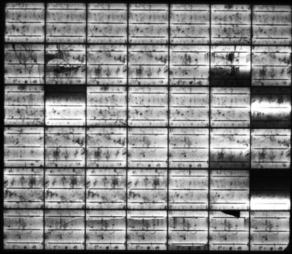
Figure 2.1 Electroluminescence (EL) picture of module with multiple broken interconnect ribbons.
PV modules and will be described in more detail in Chapter 5). The dark areas in the pic‑ ture are the regions where broken interconnect ribbons are impeding the current flow. Since the interconnects in these regions are broken, the current is no longer efficiently col‑ lected from those regions. Those regions are not producing as much energy as they should be. This module has lost approximately 10% of its initial STC power (that is peak power measured at Standard Test Conditions defined as 1000 W/m2 irradiance with the reference AM1.5 solar spectrum at a junction temperature of 25 °C.)
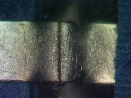
Figure 2.2 shows a picture of a broken interconnect ribbon. The module from which this ribbon was taken also had multiple dark areas in its EL picture. This particular type of module suffered from broken interconnect ribbons because of a design flaw (the ribbons were soldered to the cell edge on both front and back so there was not enough free intercon‑ nect ribbon). Many failures of interconnect ribbons are due to poor design and usually take a significant amount of time in the field (at least five years) to have a major impact on module performance. There are a number of factors in module design that facilitate inter‑ connect breakage including:
● Substrates (or superstrates) with high linear thermal expansion coefficients: If the substrate or superstrate has a high linear thermal expansion coefficient, it will expand and contract more during normal operation resulting in extra stress on the intercon nect ribbons. Values for the linear thermal expansion coefficient of some materials relevant to PV are given in Table 2.2 [2]. Substrates made of plastics, epoxy board and even metals have high thermal expansion coefficients which stresses the interconnect ribbons during outdoor exposure causing some of the ribbons to break. Many of the earliest module designs including some of the original Jet Propulsion Laboratory (JPL)Block I modules had fiber board substrates. As will be described in Chapter 4, these modules failed open circuited in a few years, with those deployed in desert