WileySeriesinQuality&ReliabilityEngineering
Dr.AndreKleyner
SeriesEditor
TheWileySeriesinQuality&ReliabilityEngineeringaimstoprovideasolid educationalfoundationforboth practitionersandresearchersintheQ&Rfieldandtoexpandthereader’s knowledgebasetoincludethelatest developmentsinthisfield.Theserieswillprovidealastingandpositive contributiontotheteachingandpracticeof engineering. Theseriescoveragewillcontain,butisnotexclusiveto,
● Statisticalmethods
● Physicsoffailure
● Reliabilitymodeling
● Functionalsafety
● Six-sigmamethods
● Lead-freeelectronics
● Warrantyanalysis/management
● Riskandsafetyanalysis
WileySeriesinQuality&ReliabilityEngineering Lead-freeSolderingProcessDevelopmentandReliability byJasbirBath(Editor) 2020
ThermodynamicDegradationScience:PhysicsofFailure,AcceleratedTesting, FatigueandReliability byAlecFeinberg October2016
DesignforSafety byLouisJ.Gullo,JackDixon February2018
NextGenerationHALTandHASS:RobustDesignofElectronicsandSystems byKirkA.Gray,JohnJ.Paschkewitz May2016
ReliabilityandRiskModels:SettingReliabilityRequirements,2ndEdition byMichaelTodinov September2015
AppliedReliabilityEngineeringandRiskAnalysis:ProbabilisticModelsand StatisticalInference byIliaB.Frenkel,AlexKaragrigoriou,AnatolyLisnianski,AndreV.Kleyner September2013
DesignforReliability
byDevG.Raheja(Editor),LouisJ.Gullo(Editor) July2012
EffectiveFMEAs:AchievingSafe,Reliable,andEconomicalProductsandProcesses UsingFailureModes andEffectsAnalysis byCarlCarlson April2012
FailureAnalysis:APracticalGuideforManufacturersofElectronicComponents andSystems byMariusBazu,TituBajenescu April2011
ReliabilityTechnology:PrinciplesandPracticeofFailurePreventioninElectronic Systems byNormanPascoe April2011
ImprovingProductReliability:StrategiesandImplementation byMarkA.Levin,TedT.Kalal March2003
TestEngineering:AConciseGuidetoCost-EffectiveDesign,Developmentand Manufacture byPatrickO’Connor April2001
IntegratedCircuitFailureAnalysis:AGuidetoPreparationTechniques byFriedrichBeck January1998
MeasurementandCalibrationRequirementsforQualityAssurancetoISO9000 byAlanS.Morris October1997
ElectronicComponentReliability:Fundamentals,Modelling,Evaluation,and Assurance byFinnJensen 1995
Editedby Mr.JasbirBath
BathConsultancyLLC 11040BollingerCanyonRoad,#E-122 SanRamon CA94582,USA
Email:Jasbir_Bath@yahoo.com
Thiseditionfirstpublished2020 ©2020JohnWiley&Sons,Inc
Allrightsreserved.Nopartofthispublicationmaybereproduced,storedinaretrievalsystem,ortransmitted, inanyformorbyanymeans,electronic,mechanical,photocopying,recordingorotherwise,exceptas permittedbylaw.Adviceonhowtoobtainpermissiontoreusematerialfromthistitleisavailableathttp:// www.wiley.com/go/permissions.
TherightofJasbirBathtobeidentifiedastheauthorofthisworkhasbeenassertedinaccordancewithlaw.
RegisteredOffice
JohnWiley&Sons,Inc.,111RiverStreet,Hoboken,NJ07030,USA
EditorialOffice 111RiverStreet,Hoboken,NJ07030,USA
Fordetailsofourglobaleditorialoffices,customerservices,andmoreinformationaboutWileyproductsvisit usatwww.wiley.com.
Wileyalsopublishesitsbooksinavarietyofelectronicformatsandbyprint-on-demand.Somecontentthat appearsinstandardprintversionsofthisbookmaynotbeavailableinotherformats.
LimitofLiability/DisclaimerofWarranty
Whilethepublisherandauthorshaveusedtheirbesteffortsinpreparingthiswork,theymakeno representationsorwarrantieswithrespecttotheaccuracyorcompletenessofthecontentsofthisworkand specificallydisclaimallwarranties,includingwithoutlimitationanyimpliedwarrantiesofmerchantabilityor fitnessforaparticularpurpose.Nowarrantymaybecreatedorextendedbysalesrepresentatives,writtensales materialsorpromotionalstatementsforthiswork.Thefactthatanorganization,website,orproductis referredtointhisworkasacitationand/orpotentialsourceoffurtherinformationdoesnotmeanthatthe publisherandauthorsendorsetheinformationorservicestheorganization,website,orproductmayprovide orrecommendationsitmaymake.Thisworkissoldwiththeunderstandingthatthepublisherisnotengaged inrenderingprofessionalservices.Theadviceandstrategiescontainedhereinmaynotbesuitableforyour situation.Youshouldconsultwithaspecialistwhereappropriate.Further,readersshouldbeawarethat websiteslistedinthisworkmayhavechangedordisappearedbetweenwhenthisworkwaswrittenandwhen itisread.Neitherthepublishernorauthorsshallbeliableforanylossofprofitoranyothercommercial damages,includingbutnotlimitedtospecial,incidental,consequential,orotherdamages.
LibraryofCongressCataloging-in-PublicationData
Names:Bath,Jasbir,editor.
Title:Lead-freesolderingprocessdevelopmentandreliability/editedby JasbirBath,BathConsultancyLLC.
Description:Firstedition.|Hoboken,NJ:JohnWiley&Sons,Inc.,2020. |Series:Wileyseriesinquality&reliabilityengineering|Includes bibliographicalreferencesandindex.
Identifiers:LCCN2020004969(print)|LCCN2020004970(ebook)|ISBN 9781119482031(hardback)|ISBN9781119482048(adobepdf)|ISBN 9781119481935(epub)
Subjects:LCSH:Electronicpackaging.|Solderandsoldering.
Classification:LCCTK7870.15.L4342020(print)|LCCTK7870.15(ebook) |DDC621.381/046–dc23
LCrecordavailableathttps://lccn.loc.gov/2020004969
LCebookrecordavailableathttps://lccn.loc.gov/2020004970
CoverDesign:Wiley
CoverImage:©PaulKrugman/Shutterstock
Setin9.5/12.5ptSTIXTwoTextbySPiGlobal,Chennai,India
PrintedintheUnitedStatesofAmerica
10987654321
Contents
ListofContributors xix
Introduction xxi
1Lead-FreeSurfaceMountTechnology 1
JenniferNguyenandJasbirBath
1.1Introduction 1
1.2Lead-FreeSolderPasteAlloys 1
1.3SolderPastePrinting 2
1.3.1Introduction 2
1.3.2KeyPastePrintingElements 2
1.4ComponentPlacement 5
1.4.1Introduction 5
1.4.2KeyPlacementParameters 5
1.4.2.1Nozzle 6
1.4.2.2VisionSystem 6
1.4.2.3PCBSupport 6
1.4.2.4ComponentSize,Packaging,andFeederCapacity 6
1.4.2.5FeederCapacity 6
1.5ReflowProcess 7
1.5.1Introduction 7
1.5.2KeyParameters 7
1.5.2.1Preheat 7
1.5.2.2Soak 8
1.5.2.3Reflow 8
1.5.2.4Cooling 9
1.5.2.5ReflowAtmosphere 9
1.6VacuumSoldering 9
1.7PasteinHole 10
1.8RoboticSoldering 11
1.9AdvancedTechnologies 12
1.9.1FlipChip 12
1.9.2PackageonPackage 12
1.10Inspection 13
1.10.1SolderPasteInspection(SPI) 13
1.10.2SolderJointInspection 14
1.10.2.1AutomatedOpticalInspection(AOI) 14
1.10.2.2X-rayInspection 15
1.11Conclusions 16 References 17
2Wave/SelectiveSoldering 19
GerjanDiepstraten
2.1Introduction 19
2.2Flux 19
2.2.1TheFunctionofaFlux 19
2.2.2FluxContents 20
2.3AmountofFluxApplicationonaBoard 20
2.4FluxHandling 21
2.5FluxApplication 21
2.5.1MethodstoApplyFlux(WaveSoldering) 21
2.5.2MethodstoApplyFlux(SelectiveSoldering) 23
2.6Preheat 24
2.6.1PreheatProcess-HeatingMethods 24
2.6.2PreheatTemperatures 27
2.6.3PreheatTime 28
2.6.4ControllingPreheatTemperatures 28
2.6.5BoardWarpageCompensation(SelectiveSoldering) 29
2.7SelectiveSoldering 29
2.7.1DifferentSelectiveSolderingPointtoPointNozzles(Selective Soldering) 29
2.7.2SolderTemperatures(SelectiveSoldering) 30
2.7.3Dip/ContactTimes(SelectiveSoldering) 31
2.7.4DragConditions(SelectiveSoldering) 31
2.7.5NitrogenEnvironment(SelectiveSoldering) 31
2.7.6WaveHeightControls(SelectiveSoldering) 32
2.7.7De-BridgingTools(SelectiveSoldering) 32
2.7.8SolderPot(SelectiveSoldering) 33
2.7.9TopsideHeatingduringSoldering(SelectiveSoldering) 34
2.7.10SelectiveSolderingDipProcesswithNozzlePlates(Selective Soldering) 34
2.7.11SolderTemperaturesforMulti-WaveDipSoldering(Selective Soldering) 35
2.7.12NitrogenEnvironment(SelectiveSoldering) 35
2.7.13WaveHeightControl(SelectiveSoldering) 36
2.7.14DipTime–ContactTimewithSolder(SelectiveSoldering) 36
2.7.15SolderFlowAccelerationandDeceleration(SelectiveSoldering) 37
2.7.16De-BridgingTools(SelectiveSoldering) 37
2.7.17Pallets(SelectiveSoldering) 38
2.7.18Conveyor(SelectiveSoldering) 38
2.8WaveSoldering 39
2.8.1WaveFormers(WaveSoldering) 39
2.8.2Pallets(WaveSoldering) 40
2.8.3NitrogenEnvironment(WaveSoldering) 40
2.8.4ProcessControl(WaveSoldering) 41
2.8.5Conveyor(WaveSoldering) 41
2.9Conclusions 42 References 42
3Lead-FreeRework 43 JasbirBath
3.1Introduction 43
3.2HandSolderingReworkforSMTandPTHComponents 43
3.2.1AlloyandFluxChoices 43
3.2.1.1Alloys 43
3.2.1.2Flux 44
3.2.2SolderingIronTipLife 44
3.2.3HandSolderingTemperaturesandTimes 47
3.3BGA/CSPRework 50
3.3.1AlloyandFluxChoices 50
3.3.1.1Alloys 50
3.3.1.2Flux 50
3.3.2BGA/CSPReworkSolderingTemperaturesandTimes 50
3.3.3ComponentTemperaturesinRelationtoIPC/JEDECJ-STD-020and Component/BoardWarpageStandards 52
3.3.3.1IPC/JEDECJ-STD-020Standard 52
3.3.3.2ComponentWarpageStandards 52
3.3.3.3BoardWarpageStandards 52
3.3.4EquipmentUpdatesforLead-FreeBGA/CSPRework 53
3.3.5AdjacentComponentTemperatures 53
3.4Non-standardComponentRework(IncludingBTC/QFN) 54
3.4.1AlloyandFluxChoices 54
x Contents
3.4.1.1Alloys 54
3.4.1.2Flux 54
3.4.2SolderingTemperaturesandTimes 54
3.4.3Non-standardComponentTemperaturesinRelationtoIPCJEDEC J-STD-020StandardandComponentWarpageStandards 55
3.4.4EquipmentandToolingUpdatesforLead-FreeNon-standard ComponentRework 55
3.4.5AdjacentComponentTemperatures 56
3.4.6Non-standardComponentReworkSolderJointReliability 56
3.5PTH(Pin-Through-Hole)WaveRework 56
3.5.1AlloyandFluxChoices 56
3.5.1.1Alloys 56
3.5.1.2Flux 57
3.5.2SolderingTemperaturesandTimes 57
3.5.3ComponentTemperaturesinRelationtoIndustryandBoardStandards DuringPTHRework 67
3.5.3.1ComponentTemperatureRatingStandards 67
3.5.3.2BareBoardTestingStandardsandMethodsforPTHRework 67
3.5.4EquipmentUpdatesforPTHComponentRework 68
3.5.5AdjacentComponentTemperaturesDuringPTHRework 68
3.5.6PTHComponentReworkSolderJointReliability 68
3.5.6.1CopperDissolution 68
3.5.6.2Holefill 69
3.6Conclusions 69 References 70
4SolderPasteandFluxTechnology 73 ShantanuJoshiandPeterBorgesen
4.1Introduction 73
4.2SolderPaste 75
4.2.1Water-SolubleSolderPaste 75
4.2.2No-CleanSolderPaste 76
4.3FluxTechnology 77
4.3.1Halide-FreeandHalide-Containing 77
4.4CompositionofSolderPaste 79
4.4.1Alloy 79
4.4.2Flux 82
4.4.3SolderPowderType 83
4.4.3.1OxideLayer 84
4.5CharacteristicsofaSolderPaste 84
4.5.1Printing 84
4.5.1.1PrintingParameters 85
4.5.2Reflow 86
4.5.2.1Wetting/SpreadabilityofLead-FreeSolderPaste 86
4.5.2.2Bridging 86
4.5.2.3MicroSolderBalls 86
4.5.2.4Voiding 86
4.5.2.5Head-on-PillowComponentSolderingDefect 88
4.5.2.6Non-WetOpen 90
4.5.2.7Tombstoning 90
4.5.3In-CircuitTest(ICT)ProbeTestability 90
4.5.4FluxReliabilityIssues 91
4.6Conclusions 92 References 92
5LowTemperatureLead-FreeAlloysandSolderPastes 95 RaiyoAspandiar,NileshBadwe,andKevinByrd
5.1Introduction 95
5.1.1DefinitionofLowTemperatureSolders 95
5.1.2BenefitsofLowTemperatureSoldering 97
5.1.2.1ReducedManufacturingCost 98
5.1.2.2PowerUseSavings 98
5.1.2.3EnvironmentalBenefits 99
5.1.2.4ManufacturingYieldImprovements 100
5.1.3Drawbacks 103
5.1.3.1Brittleness 103
5.1.4OtherLowTemperatureMetallurgicalSystems 103
5.2DevelopmentofRobustBismuth-BasedLowTemperatureSolder Alloys 105
5.2.1Bismuth-Tin(Bi-Sn)PhaseDiagram 105
5.2.2MechanicalProperties 107
5.2.3PhysicalProperties 108
5.2.4AlloyDevelopmentProgress 108
5.2.5FluxesforLowTemperatureSolders 109
5.3SMTProcessCharacterizationofSn-BiBasedSolderPastes 111
5.3.1Printability 111
5.3.2ReflowProfiles 112
5.3.3Rework 113
5.4PolymericReinforcementofSn-BiBasedLowTemperature Alloys 114
5.4.1CurrentPolymericReinforcementStrategies 114
5.4.2JointReinforcedPastes(JRP) 118
5.4.3PolymericReinforcementSummary 128
5.5MixedSnAgCu-BiSnBGASolderJoints 128
5.5.1FormationMechanism 128
5.5.2MicrostructuralFeaturesandKeyCharacteristics 133
5.5.3SolderingProcessOptimization 134
5.5.4PossibleDefects 135
5.6SolderJointReliability 140
5.7Conclusions 145
5.8FutureDevelopmentandTrends 146 References 149
6HighTemperatureLead-FreeBondingMaterials–TheNeed, thePotentialCandidatesandtheChallenges 155 HongwenZhangandNing-ChengLee
6.1Introduction 155
6.2SolderMaterials 159
6.2.1Gold-BasedSolders 159
6.2.2Bismuth-RichSolders 160
6.2.2.1DesignofBismuth-RichSolders 160
6.2.2.2MechanicalBehaviorofBiAgX 163
6.2.2.3MicrostructureandMicrostructuralEvolutionofBiAgXJoint 167
6.2.3Tin-Antimony(Sn-Sb)HighTemperatureSolders 174
6.2.4Zinc-AluminumSolders 176
6.3Silver(Ag)-SinteringMaterials 178
6.4TransientLiquidPhaseBondingMaterials/Technique 181
6.5Summary 182 Acknowledgment 185 References 185
7Lead(Pb)-FreeSoldersforHighReliabilityand High-PerformanceApplications 191 RichardJ.Coyle
7.1EvolutionofCommercialLead(Pb)-FreeSolderAlloys 191
7.1.1FirstGenerationCommercialPb-FreeSolders 191
7.1.2SecondGenerationCommercialPb-FreeSolders 192
7.1.3ThirdGenerationCommercialPb-FreeSolders 196
7.2ThirdGenerationAlloyResearchandDevelopment 196
7.2.1LimitationsofSn-Ag-CuSolderAlloys 196
7.2.2EmergenceofCommercialThirdGenerationAlloys 202
7.2.2.1TheGenesisof3rdGenerationAlloyDevelopment 202
7.2.2.2AnExpandingClassof3rdGenerationAlloys 202
7.2.3MetallurgicalConsiderations 203
7.2.3.1Antimony(Sb)AdditionstoTin(Sn) 206
7.2.3.2Indium(In)AdditionstoTin(Sn) 207
7.2.3.3Bismuth(Bi)AdditionstoTin(Sn) 209
7.3ReliabilityTestingThirdGenerationCommercialPb-FreeSolders 210
7.3.1ThermalFatigueEvaluations 210
7.3.2iNEMI/HDPUGThirdGenerationAlloyPb-FreeThermalFatigue Project 213
7.3.3MicrostructureandReliabilityofThirdGenerationAlloys 219
7.4ReliabilityGapsandSuggestionsforAdditionalWork 223
7.4.1RootCauseofInterfacialFractures 223
7.4.2EffectofComponentAttributesonThermalFatigue 224
7.4.3EffectofSurfaceFinishonThermalFatigue 224
7.4.4ThermomechanicalTestParametersandTestOutcomes 225
7.4.4.1ThermalCyclingDwellTime 225
7.4.4.2Preconditioning(IsothermalAging) 225
7.4.4.3ThermalCyclingofMixedMetallurgyBGAAssemblies 226
7.4.4.4ThermalShockorAggressiveThermalCycling 226
7.4.5ReliabilityUnderMechanicalLoading:Drop/Shock,and Vibration 227
7.4.6SolderAlloyMicrostructureandReliability 230
7.4.7SummaryofSuggestionsforAdditionalInvestigation 231
7.5Conclusions 232 Acknowledgments 234 References 234
8Lead-FreePrintedWiringBoardSurfaceFinishes 249 RickNichols
8.1Introduction:WhyaSurfaceFinishIsNeeded 249
8.2SurfaceFinishesintheMarket 250
8.3ApplicationPerspective 255
8.4ADescriptionofFinalFinishes 261
8.4.1HotAirSolderLeveling(HASL) 263
8.4.1.1ProcessComplexity 263
8.4.1.2ProcessDescription 265
8.4.1.3IssuesandRemedies 267
8.4.1.4Summary 267
8.4.2HighTemperatureOSP 267
8.4.2.1ProcessComplexity 267
8.4.2.2ProcessDescription 269
8.4.2.3IssuesandRemedies 270
8.4.2.4Summary 270
8.4.3ImmersionTin 271
8.4.3.1ProcessComplexity 271
8.4.3.2ProcessDescription 273
8.4.3.3IssuesandRemedies 275
8.4.3.4Summary 276
8.4.4ImmersionSilver 276
8.4.4.1ProcessComplexity 277
8.4.4.2ProcessDescription 279
8.4.4.3IssuesandRemedies 280
8.4.4.4Summary 281
8.4.5ElectrolessNickelImmersionGold(ENIG) 281
8.4.5.1ProcessComplexity 281
8.4.5.2ProcessDescription 283
8.4.5.3IssuesandRemedies 285
8.4.5.4Summary 286
8.4.6ElectrolessNickel/ElectrolessPalladium/ImmersionGold (ENEPIG) 287
8.4.6.1ProcessComplexity 287
8.4.6.2ProcessDescription 289
8.4.6.3IssuesandRemedies 290
8.4.6.4Summary 291
8.4.7ElectrolessNickelAutocatalyticGold(ENAG) 291
8.4.7.1ProcessComplexity 292
8.4.7.2ProcessDescription 293
8.4.7.3IssuesandRemedies 295
8.4.7.4Summary 295
8.4.8ElectrolessPalladiumAutocatalyticGold(EPAG) 295
8.4.8.1ProcessComplexity 295
8.4.8.2ProcessDescription 297
8.4.8.3IssuesandRemedies 298
8.4.8.4Summary 299
8.4.9ElectrolyticNickelElectrolyticGold 299
8.4.9.1ProcessComplexity 299
8.4.9.2ProcessDescription 301
8.4.9.3IssuesandRemedies 301
8.4.9.4Summary 302
8.5Conclusions 303 References 304
9PCBLaminates(IncludingHighSpeedRequirements) 307 KarlSauterandSilvioBertling
9.1Introduction 307
9.2ManufacturingBackground 307
9.3PCBFabricationDesignandLaminateManufacturingFactors AffectingYieldandReliability 308
9.3.1HighFrequencyLoss 308
9.3.2MixedDielectric 308
9.3.3Back-Drilling 309
9.3.4AspectRatio 309
9.3.5PCBFabrication 309
9.3.6PressLamination 310
9.3.7MoistureContent 310
9.3.8LaminateMaterial 311
9.4AssemblyFactorsAffectingYieldsandLong-TermReliabilityfor LaminateMaterials 311
9.4.1ReflowTemperature 311
9.4.2AssemblyComponents 312
9.4.3ThermalStress 312
9.5CopperFoilTrends(bySilvioBertling) 312
9.6HighFrequency/HighSpeedandOtherTrendsAffectingLaminate Materials 316
9.6.1HighSpeedStandards 316
9.6.2AdhesionTreatment(PriortoPressLamination) 317
9.6.3LaminateMaterialFillerContent 317
9.6.4GlassWeaveEffect 317
9.6.5Halogen-Free 318
9.7Conclusions 318 References 319
10UnderfillsandEncapsulantsUsedinLead-FreeElectronic Assembly 321 BrianJ.Toleno
10.1Introduction 321
10.2Rheology 322
10.2.1RheologicalResponseandBehavior 323
10.2.1.1Thixotropy 325
10.2.2MeasuringRheology 327
10.2.2.1SpindleTypeViscometry 327
10.2.2.2ConeandPlateRheometry 328
10.3CuringofAdhesiveSystems 330
10.3.1ThermalCure 330
10.3.2Ultraviolet(UV)LightCuring 335
10.3.3MoistureCure 338
10.4GlassTransitionTemperature 339
10.5CoefficientofThermalExpansion(CTE) 341
10.6Young’sModulus(E) 343
10.7Applications 344
10.7.1Underfills 344
10.7.1.1CapillaryUnderfill 345
10.7.1.2Fluxing(No-Flow)Underfill 348
10.7.1.3Removable/ReworkableUnderfill 349
10.7.1.4StakingorCornerBondUnderfill 349
10.7.2EncapsulantMaterials 350
10.7.2.1GlobTop 351
10.7.2.2ComponentEncapsulation 351
10.7.2.3Application 353
10.7.2.4Low-PressureMolding 355
10.8Conclusions 355 References 355
11ThermalCyclingandGeneralReliability Considerations 359 MaximSerebreni
11.1IntroductiontoThermalCyclingofElectronics 359
11.1.1InfluenceofSolderAlloyCompositionandMicrostructureonThermal CyclingReliability 362
11.2InfluenceofPackageTypeandThermalCyclingProfile 363
11.2.1InfluenceofBoardandPadDesign 366
11.3FatigueLifePredictionModels 371
11.3.1EmpiricalModelsandAccelerationFactors 371
11.3.2Semi-empiricalModels 372
11.3.3FiniteElementAnalysis(FEA)BasedFatigueLifePredictions 373
11.4Conclusions 376 References 377
12IntermetallicCompounds 381
AlyssaYaeger,TravisDale,ElizabethMcClamrock,GaneshSubbarayan, andCarolHandwerker
12.1Introduction 381
12.1.1Solders 382
12.1.2InteractionwithSubstrates 382
12.2SettingtheStage 384
12.2.1MechanicalandThermomechanicalResponseofSolderJoints 386
12.3CommonLead-FreeSolderAlloySystems 392
12.3.1SolderJointsFormedBetweenSn-Cu,Sn-Ag,andSn-Ag-CuSolder AlloysandCopperSurfaceFinishes 396
12.3.1.1Sn-CuSolderonCopper 396
12.3.1.2Sn-AgandSn-Ag-CuSolderAlloysonCopper 399
12.3.2SolderJointsFormedBetweenSn-Cu,Sn-Ag,andSn-Ag-CuAlloysand NickelSurfaceFinishes 408
12.3.2.1Ni-Sn 408
12.3.2.2Sn-AgSolderAlloysonNickel 411
12.3.2.3Spalling 415
12.3.2.4EffectsofPhosphorusConcentrationinENIGonSolderJoint Reliability 416
12.3.3Au-Sn 417
12.4HighLead–Exemption 422
12.5Conclusions 423 References 423
13ConformalCoatings 429 JasonKeeping
13.1Introduction 429
13.2Environmental,Health,andSafety(EHS)Requirements 430
13.3OverviewofTypesofConformalCoatings 430
13.3.1TypesofConformalCoatings 431
13.3.1.1AcrylicResins(TypeAR) 432
13.3.1.2UrethaneResins(TypeUR) 433
13.3.1.3EpoxyResins(TypeER) 433
13.3.1.4SiliconeResins(TypeSR) 435
13.3.1.5Para-xylylene(TypeXY) 436
13.3.1.6SyntheticRubber(TypeSC) 437
13.3.1.7Ultra-Thin(TypeUT) 438
13.4PreparatoryStepsNecessarytoEnsureaSuccessfulCoating Process 440
13.4.1AssemblyCleaning 440
13.4.2AssemblyMasking 440
13.4.3PrimingandOtherSurfaceTreatments 441
13.4.3.1MeasuringSurfaceEnergy 441
13.4.3.2WaterDropContactAngle 447
13.4.4Bake-Out 448
13.5VariousMethodsofApplyingConformalCoating 449
13.5.1ManualCoating 449
13.5.2Dip 449
13.5.3HandSpray 450
13.5.4AutomaticSpray 451
13.5.5SelectiveCoating 451
13.5.6VaporDeposition 451
13.6AspectsforCure,Inspection,andDemasking 453
13.6.1Cure 453
13.6.1.1SolventEvaporation 453
13.6.1.2RoomTemperatureVulcanization(RTV) 454
13.6.1.3HeatCure 454
13.6.1.4UVCure 454
13.6.1.5Catalyzed 454
13.6.2UVInspection 455
13.6.3Demasking 455
13.7RepairandReworkProcesses 456
13.7.1Chemical 456
13.7.2Thermal 456
13.7.3Mechanical 457
13.7.4Abrasion(Micro-Abrasion) 457
13.7.5PlasmaEtch 457
13.8DesignGuidanceonWhenandWhereConformalCoatingisRequired, andWhichPhysicalCharacteristicsandPropertiesareImportantto Consider 457
13.8.1IsConformalCoatingRequired? 458
13.8.1.1WhyUseIt? 458
13.8.1.2WhyNotUseConformalCoating? 459
13.8.2DesirableMaterialProperties 459
13.8.3AreastoMask 461
13.9Long-TermReliabilityandTesting 462
13.10Conclusions 462
13.11FutureWork 463 References 463
Index 467
ListofContributors
RaiyoAspandiar IntelCorporation
Hillsboro,OR USA
NileshBadwe IntelCorporation
Hillsboro,OR USA
JasbirBath BathConsultancyLLC SanRamon,CA USA
SilvioBertling Mesa Arizona,USA
PeterBorgesen IntegratedElectronicsEngineering Center
BinghamtonUniversity,State UniversityofNewYork,NY USA
KevinByrd IntelCorporation Hillsboro,OR USA
RichardJ.Coyle NokiaBellLaboratories MurrayHill,NJ USA
TravisDale SchoolofMechanicalEngineering PurdueUniversity WestLafayette,IN USA
GerjanDiepstraten VitronicsSoltec Oosterhout,TheNetherlands
CarolHandwerker SchoolofMaterialsEngineering PurdueUniversity WestLafayette,IN USA
xx ListofContributors
ShantanuJoshi KokiSolderAmerica
Cincinnati,OH
USA
JasonKeeping CelesticaInc. Toronto Canada
Ning-ChengLee IndiumCorporation Clinton,NY USA
ElizabethMcClamrock SchoolofMaterialsEngineering PurdueUniversity WestLafayette,IN USA
JenniferNguyen Flex Milpitas,California USA
RickNichols Atotech Berlin Germany
GaneshSubbarayan SchoolofMechanicalEngineering PurdueUniversity WestLafayette,IN USA
KarlSauter OracleCorporation SantaClara,California USA
MaximSerebreni DepartmentofMechanical Engineering UniversityofMaryland CollegePark,MD USA
BrianJ.Toleno Microsoft MountainView,California USA
AlyssaYaeger SchoolofMaterialsEngineering PurdueUniversity WestLafayette,IN USA
HongwenZhang IndiumCorporation Clinton,NY USA
Introduction
Withthemovementtolead-freesolderinginelectronicsmanufacturingproduction,thereisaneedforanupdatedreviewofvarioustopicsinthisareaforpracticingprocess,qualityandreliabilityengineersandmanagerstobeabletouseto addressissuesinproduction.
Thebookgivesupdatesinareasforwhichresearchisongoing,andaddresses newtopicswhicharerelevanttolead-freesoldering.Itcoversalistofkeytopics includingdevelopmentsinprocessengineering,alloys,printedcircuitboard(PCB) surfacefinishes,PCBlaminates,andreliabilityassessments.
Chapter1discusseslead-freesurfacemounttechnology(SMT)withreviewof thesurfacemountprocessforlead-freesoldering,includingprinting,component placement,reflow,inspection,andtest.
Chapter2coverslead-freeselectiveandwavesolderingintermsoffluxandpreheatprocessesaswellasthesimilaritiesanddifferencesoftheseprocesses.
Chapter3discussestheissuesduringlead-freereworkfortheassembledcomponentsbasedonthehigherlead-freesolderingtemperaturesandtherangeofsmall andlargecomponentstoreworkaswellastemperatureandmoisturesensitivitywithcomponentsandboards.Thechapterreviewsupdatesinlead-freerework technologyincludinghandsoldering,ballgridarray/chipscalepackageBGA/CSP rework,andPTH(PinThroughHole)rework.
Chapter4discusseslead-freesolderpasteandfluxtechnologyandthecharacteristicsneededforthesematerialstoensuregoodsolderpasteperformance.Italso reviewsthedefectswhichcanoccurduringelectronicsmanufacturing,includingmicrosolderballs,voiding,tombstoning,bridging,opens,head-on-pillow,and non-wetopens.
Chapter5coverslowtemperaturelead-freealloysandpastes,withanemphasis ontheBi-Snsystemandthedevelopmentworkongoinginthisarea.
Chapter6discussessoldermaterials,silver-sinteringmaterials,andTLPB(transientliquidphasebonding)materialsasthethreepotentialcandidatetypesfor lead-free,high-temperature,die-attachmentmaterials.
Chapter7coversthedrivers,benefits,andconcernsassociatedwiththedevelopmentandimplementationofthirdgeneration,highreliabilitylead-freesolders.
Chapter8reviewslead-freesurfacefinishalternatestotheelectrolyticnickel immersiongoldsurfacefinishinrelationtoperformancecharacteristicsandcost, withselectionofafinalboardsurfacefinishbeingofsignificancetotheassembly andreliabilityoftheproduct.
Chapter9discussesseveralcriticalfactorsrelatingtoPCBlaminatematerials anddescribeswhytheyareimportanttoensuringthatthefinishedboardperformancerequirementsaremet.
Chapter10reviewstheuseofadhesivesinthemanufacturingofhigh-density lead-freesurfacemountassemblies,withadiscussionofthetwoadhesiveapplicationsusedwidelyforincreasedreliability:underfillsandencapsulants.
Chapter11overviewsthermalcyclingreliabilityinrelationtolead-freesolder joints,withthereliabilityofsolderinterconnectsinfluencedbyallaspectsofthe electronicassembly,rangingfromthecomponentpackagestyleandcircuitboard constructiontothesoldercomposition.
Chapter12discussesintermetalliccompounds(IMCs)formedinthelead-free solderjointswithadiscussionoftherolesthatIMCsplayindeterminingsolder jointreliability,andhowthoseroleschangeasaresultofagingordamageinduced bythermalcycling.Itcoverstheperformanceofcommonlead-freesolderalloys incombinationwithmetallizationsandsurfacefinishestounderstandwhatto expectinthesespecificsystemsandtheproblemsthatmayarisewhencombining newsolderalloysandsurfacefinishes/metallizationsandthemethodologiesthat canbeusedtoseparateoutthedifferentpossiblerootcauses.
Thefinalchapter(Chapter13)coversindustryupdatesintheuseofconformal coatingsandtheiruseinelectronicsmanufacturingandtheireffectonreliability.Variousaspectsofconformalcoatingsarediscussed,includingEnvironmental HealthandSafety(EHS)requirements,thefivebasicconformalcoatingtypesand newemergingmaterials,preparation,application,cure,andinspectionofconformalcoatings,repairandrework,anddesignguidanceonwhenandwherecoatings arerequired,andwhichphysicalcharacteristicsandpropertiesareimportantto consider.
Lead-FreeSurfaceMountTechnology
JenniferNguyen 1 andJasbirBath 2
1 Flex,Milpitas,California,USA
2 BathConsultancyLLC,SanRamon,CA,USA
1.1Introduction
Surfacemounttechnology(SMT)involvestheassemblyorattachmentofsurface mountdevices(SMDs)ontotheprintedcircuitboard(PCB).Today,themajority oftheproductsarebuiltusingsurfacemounttechnologyandlead-freeprocess. Thischapterwillreviewthesurfacemountprocessforlead-freesoldering,includingprinting,componentplacement,reflow,inspection,andtest.Thechapteralso discussessomeadvancedminiaturizationtechnologiesusedintheSMTprocess.
1.2Lead-FreeSolderPasteAlloys
Today,thereareavarietyoflead-freesolderpastealloysavailableinthemarket. SnAgCu(SAC)materialswith3.0–4.0%Agand0.5–0.9%CuandremainderSn arewidelyacceptedwithintheindustry.Amongthem,Sn3.0Ag0.5Cu(SAC305) isstillthemostcommonalloyusedintheSMTprocess.TheseSnAgCualloys havetheliquidustemperatureofaround217 ∘ C.AsthecostofAghasincreased overthepastyears,theuseoflowAgalloymaterialssuchasSn0.3-1.0AgCuor SnCu/SnCuNihasincreased.Thesealloyshaveapproximately10 ∘ ChighermeltingtemperaturethanSAC305andmayneedtobeprocessedatslightlyhigher temperatureduringthereflowprocess.
Lowtemperaturelead-freealloyswhichcontainSnBi/SnBiAgarealsoused. Thesealloyshavemeltingtemperaturearound140 ∘ Candcanbeprocessedat 170–190 ∘ C.Theselowtemperaturealloysusuallyhavehighbismuthcontentand theycreatesomereliabilityconcerns,especiallyonmechanicalreliability.These Lead-freeSolderingProcessDevelopmentandReliability, FirstEdition.EditedbyJasbirBath. ©2020JohnWiley&Sons,Inc.Published2020byJohnWiley&Sons,Inc.
1Lead-FreeSurfaceMountTechnology
lowtemperaturealloysareusedoncertainapplicationssuchaslight-emitting diode(LED)/TVproducts.Inrecentyears,thereisadesireforlowtemperature lead-freealloyalternativeswithbetterreliability.Thedriversfortheselow temperaturealloysincludecomponentwarpage,lowenergyconsumption,and componentorboardsensitivitytothehighertemperaturelead-freeprocess.These alloystypicallyhavehigherliquidustemperaturethantraditionalSnBi/SnBiAg alloys,buttheystillhavelowerliquidustemperaturethanSAC305.Thesealloys havegainedalotofinterestintheindustryintherecentyears,andsomeare availableinthemarketandusedinproduction.
1.3SolderPastePrinting
1.3.1Introduction
OneofthemostimportantprocessesofthesurfacemountassemblyistheapplicationofsolderpastetothePCB.Thisprocessmustaccuratelydepositthecorrectamountofsolderpasteontoeachofthepadstobesoldered.Screen-printing thesolderpastethroughafoilorstencilisthemostcommonlyusedtechnique, althoughothertechniquesuchasjetprintingisalsoused.
Thereisnomajorchangetosolderpasteprintingforlead-freeprocesses.The sameprintercanbeusedfortin-leadandlead-freeprinting.Ingeneral,thesame stencildesignguidelinescanbeusedforlead-freeprocess.
1.3.2KeyPastePrintingElements
Solderpasteprintingprocessisoneofthemostimportantprocessesinsurface mounttechnology.Thisprocesscanaccountforthemajorityoftheassembly defectsifitisnotcontrolledproperly.Foreffectivesolderpasteprinting,the followingkeyfactorsneedtobeoptimizedandcontrolled:
● PCBsupport
● Squeegee(type,speed,pressure,angle)
● Stencil(thickness,aperture,cleanliness,snapoff,separationspeed)
● Solderpaste(includingtype,viscosity)
PCBsupportisimportanttotheprintingprocess.GoodPCBsupportholdsthe PCBflatagainstthestencilduringthescreen-printingprocess.PCBsupportisgenerallyprovidedwiththescreen-printingmachines.Iftheboardisnotproperly supported,solderdefectssuchasbridging,insufficientsolder,andsoldersmearingcanbeseen.Forfinepitchprintingsuch0.3/0.4mmpitchchipscalepackage (CSP),0201/01005(Imperial)chipcomponent,adedicatedcustom-madefixture forprintingorvacuumsupportshouldbeused.
Squeegees,squeegeepressure,andspeedareothercriticalparametersinthe screen-printingprocess.Metalsqueegeesarecommonlyusedforprintingsolder paste,andrubberorpolyurethanesqueegeesareusedforepoxyprinting.A squeegeeangleof60 ∘ Ctothestencilistypicallyused[1].Squeegeespeedand squeegeepressurearecriticalforgoodprinting.Thespeedofthesqueegeedetermineshowmuchtimethesolderpastecanrollandsettleintotheaperturesofthe stencilandontothepadsofthePCB.Inthebeginningoflead-freeconversion, aslowerprintingspeedwasusedbecausethelead-freesolderpastewasstickier thantin-leadsolderpaste.Today,manylead-freesolderpastescanprintwellat highspeed.
Thespeedsettingiswidelyvariedfromatypicalrangeof20–100mm/s 1 dependingonthesizeoftheaperture,thesizeofPCB,andthequantityofboards beingassembled,etc.Printingspeeduseddependsonthesolderpastesupplier orisoptimizedbyaDesignofExperiment(DOE).Itistypicallybetween40and 80mms 1 .Duringthesolderpasteprinting,itisimportanttoapplysufficient squeegeepressureandthispressureshouldbeevenlydistributedacrossthe entiresqueegees.Toolittlepressurecancauseincompletesolderpastetransfer tothePCBorpastesmearing.Toomuchpressurecancausethepastetosqueeze betweenthestencilandthepad.
Stencilisanotherkeyfactorinthesolderpasteprinting.Metalstencilsareused insolderpasteprinting.Stainlesssteelmaterialiscommonlyused;however,metal stencilscanbemadeofcopper,bronze,ornickel[2].Thereareseveraltypesof screen-printingstencil,includingchemicaletch,lasercut,andelectroformed[2].
Thethicknessofthestencilistypically125 μm(5mil)or150 μm(6mil).Stencils withthethicknessof100 μm(4mil)orthinnerhavebecomemorepopularwith thehighdensityandfinepitchcomponentssuchas0201/01005(Imperial)chip componentsor0.4/0.3mmpitchCSPorquadflatno-leads/bottomtermination component(QFN/BTC)components.Thickerstencilsthan150 μmaretypically usedwhenmorepasteisneeded.Stencilthicknessandaperturesizedeterminethe amountofpastedepositedonthepad.Ingeneral,stencilaperturemustbethree timesandpreferablyfivetimesthediameterofthesolderparticles.Toensurethe properpastereleaseandefficientprinting,theaspectratioshouldbegreaterthan 1.5,andthearearatioshouldbegreater0.66.
TheaspectratioisdefinedbyEq.(1.1),andthearearatioisshowninEq.(1.2).
Aspectratio = ApertureWidth∕StencilThickness(1.1)
AreaRatio = AreaoftheAperture (L × W)∕AreaofApertureWalls (2 ×(L + W)× T) (1.2)
Snapoffandstencilseparationspeedarealsoimportantforgoodprintingquality.SnapoffisthedistancebetweenthestencilandthePCB.Formetalstencil
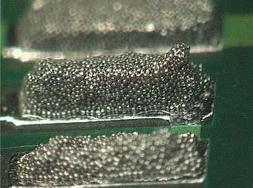
Exampleoftailingattheedgeofthepasteduetohighseparationspeed. printing,thesnapoffshouldbezero.Thisisalsocalledcontactprinting.Ahigh snapoffwillresultinathickerlayerofsolderpaste.Stencilseparationspeedisthe speedofseparationbetweenthestencilandPCBafterprinting.Traditionally,high separationspeedwillresultincloggingofthestencilaperturesortailingatedges aroundthesolderpastedeposited(Figure1.1).However,lead-freepastestendto haveahigheradherencethantin-leadpastesandmaypreferhighseparationspeed thantin-leadsolderpaste.Separationspeedvariesdependingonthesolderpastes anditssupplier,andthesupplier’srecommendationshouldgenerallybefollowed. Lastbutnotleast,thecorrectsolderpastetypeandmaterialshouldbeused.The correcttypeofsolderpasteshouldbeselectedbaseduponthesizeoftheapertures withinthestencil.Type3wascommonlyusedinthetin-leadprocess;however, Type4hasbecomeamorecommonlead-freesolderpastetypeintherecentyears duetotheincreaseinminiaturizedcomponentsontheprintedcircuitboard.The
Figure1.1
Table1.1 Generalsolderpaste typeandparticlesizes.
releasefromtheaperturesofthestencilisaffectedbytheparticlesizewithinthe selectedsolderpaste.Table1.1liststheparticlesizeofdifferentsolderpastetype. Bothtin-leadandlead-freesolderpasteshouldberefrigeratedwhilebeingstored tomaintainitsshelflifebutmustbebroughttoroomtemperaturebeforeuseto maintainquality.Somenewlead-freesolderpastesrequirenorefrigerationand canbestoredatroomtemperature.Thesolderpasteshouldbemixedproperly beforeusetoensureevendistributionofanyseparatedmaterialthroughoutthe paste.Itisrecommendedtofollowthesolderpastemanufacturer’srecommendationsforstorageandhandlingconditions.
1.4ComponentPlacement
1.4.1Introduction
Afterthecorrectamountofsolderpasteisapplied,componentsareplacedonthe PCBatthespecificlocations.Thecomponentplacementprocessincludesboard loadingandregistration,fiducialvisionalignment,componentpick-up,componentinspection,andalignmentandplacement.Thecomponentplacementmust bepreciseandinaccordancewiththeschematics.Pickandplacemachinesare usedinthisprocess.Therearedifferenttypesofpickandplacementmachineavailableinthemarket.Somemachinesaredesignedspecificallyforspeedwhereas othersaremorefocusedonflexibility.Themachinesdesignedforspeedaregenerallyreferredtoas“chipshooters”andcanachievecomponentplacementrates ofupto100000cph(componentsperhour).Theflexiblepickandplacemachine canhandlecomponentsrangingfrom01005(Imperial)chipstolargecomponents suchasballgridarrays(BGAs),connectors,etc.Flexiblemachinestypicallyhave slowerpickandplacespeedthanthechipshooter.Themachinesareselected dependingonthetypes,sizes,andvolumesofthesurfacemountcomponents.The samepickandplaceequipmentcanbeusedfortin-leadandlead-freecomponents.
1.4.2KeyPlacementParameters
Componentplacementisanimportantfactorinsurfacemountassembly.Itaffects notonlytheassemblytimebutalsothereliabilityofthesolderjoint.Placement accuracyandplacementspeedarecriticalinthisprocess.Toachieveaccurate placementandhighoutput,thefollowingfactorsneedtobeconsidered:
● Nozzle
● Visionsystem
● PCBsupport
● Componentsize,packaging
● Feedercapacity
1.4.2.1Nozzle
Itisveryimportantthatthecorrectnozzlebeselectedforeachdifferentpartto beplacedtoensureaccurateandconsistentplacement.Therearemanydifferenttypesofnozzleforpickandplacecomponents.Mostnozzlesuseavacuumto holdthecomponents.Forhandlingsmallcomponents,positivepressureisoften suppliedinadditiontovacuumatthemomentofplacementsothatthecomponentwouldbecompletelyreleasedfromthenozzle.Componentflatnessatthetop surfaceisimportantforthepickandplaceprocess.Certaincomponentssuchas connectorsthatdonothaveaflattopsurfacecanhaveapick-uppadinsertedor pre-attachedbythesupplierforpickandplacepurposes.Somealternativenozzles haveagripper,whichgripsthecomponentsidesinstead.Thegripperistypically forplacingsomeodd-shapedcomponents.However,theplacementspeedistypicallyslowerascomparedtothenozzlesthatholdthecomponentbyvacuum.In addition,extraspaceisrequiredbetweenthecomponentstoaccommodatethe grippers.
1.4.2.2VisionSystem
Thevisionsysteminspectseverycomponentbeforeplacement.Itchecksthepart dimensionsandanycomponentdamagebeforeplacement.Itisimportanttoprogrameachcomponentwiththecorrecttoleranceparameterstoallowthemachine todetermineifanincorrectparthasbeenloadedandalsonottorejectacceptable components.
1.4.2.3PCBSupport
ThePCBneedstohaveadequatesupportduringcomponentplacement.Improper PCBsupportcancausecomponentmisalignmentormissingcomponents.
1.4.2.4ComponentSize,Packaging,andFeederCapacity
ThesurfacemountcomponentsonthePCBwilldifferinsize.Itiscommontohave smallcomponentspositionedclosetolargecomponentsinhighdensitydesign.All smallcomponentsneedtobeplacedbeforelargercomponentssothatthelarger componentsdonotgetdisturbedandmisalignedduringplacement.
Thesurfacemountcomponentsaresuppliedindifferentways.Themostcommoncomponentpackagesaretapeandreel,tubes,andtrays.
1.4.2.5FeederCapacity
Feedersareusedtofeedcomponentstoafixedlocationforthepick-upmechanism.Feedertypesincludetapeandreelfeeder,matrixtrayfeeder,bulkfeeder, andtubefeeder.Thetapeandreelfeederscomeindifferentsizesandarethemost commonfeederforplacinglargequantitiesofsmallcomponents.Thenumberof tapefeedersthatcanbeloadedintothemachineatatimewillplayanimportant
roleindeterminingthespeedofcomponentplacement.Thematrixtrayfeedersare typicallyusedforlargeand/orexpensivecomponentssuchasBGAorQFN/BTC components.Thetrayholdsthecomponentssecurelywithoutdamagingthebody orleads.However,thepickandplaceprocessforthetrayfeederisoftenslower thanthetapefeeder.
1.5ReflowProcess
1.5.1Introduction
Inreflowsoldering,thesolderpasteandsolderballsforthecaseofaBGAcomponentmustbeheatedsufficientlyaboveitsmeltingpointandbecomecompletely molten,inordertoformreliablejoints.Inthecaseofcomponentswithleads,the solderpastemustwettheplatingoncomponentleadstoformthedesiredheeland toefillets.
Thereisnoonebestreflowprofileforallboardassemblies.Ideally,areflow profilemustbecharacterizedforeachboardassemblyusingthermocouplesat multiplelocationsonandaroundthecomponentdevicesandboard.Thesolder pastetype,component,andboardthermalsensitivitymustbeconsideredinreflow profiledevelopment.
Lead-freesolderstypicallyprocessathighertemperaturethantin-leadsolder duetothehighmeltingtemperatureoftypicallead-freesolders.Lead-freesolder suchasSAC305(Sn3Ag0.5Cu)haveaninitialmeltingpointof217 ∘ Candafinal meltingpointof220 ∘ C.Lead-freereflowtypicallyhasanarrowerprocesswindowthantin-leadreflowduetothecomponentorboardmaximumtemperature limitations.
1.5.2KeyParameters
Solderjointformationdependsontemperatureandtimeduringreflow.Thereare fourphasesofareflowprocess,includingpreheat,soak,reflow,andcooling.In addition,reflowatmosphereplaysanimportantroleinthereflowprocess.The keyparametersforreflowwillbediscussedinthefollowingsections.
1.5.2.1Preheat
ThepreheatphasepreparesthePCBandcomponentsforactualreflow.Ithelps toreducethethermalshockandtemperaturedifferencebetweenthePCBand componentsandreflowtemperature.Aquickramprateduringthepreheatcan damagethecomponent.Ingeneral,arampratebetween1.0and3.0 ∘ C/s 1 isrecommended,andthetemperaturechangeshouldbeevenlydistributedthroughout thePCB.Preheatalsoremovessomefluxvolatilesandpreparesthesolderpaste materialforreflow.
1.5.2.2Soak
Soakisalsoknownasthepre-reflowphase.Inthisphase,thefluxinthesolder pastegetsactivated,andthishelpstoremoveoxidationonthecomponentleads, PCBpadsoronthesolderparticles’surface.Also,soakingphaseallowsthe thermalgradientacrossthePCBtoequilibratepriortoreflow.Inthisway,the entireassemblyseesnearlythesamereflowconditionstoformconsistentsolder bonds.Forlargeboardsorboardswithalargerangeofcomponentsizes,alonger soaktimeisusuallyhelpfultoachievesuccessfulassemblytohelpensurethe deltaTemperatureacrosstheboardisreduced.Soakprofilesarealsousedto minimizevoidingwhenassemblingsuchcomponentsasBGA,landgridarray (LGA),andQFN/BTC.
1.5.2.3Reflow
Asthesolderreachesthesoldermeltingtemperature,theboardentersthereflow phase.Peaktemperatureandtimeaboveliquidustemperatureareimportantfactorsinthisphase.Thepeaktemperatureisgenerally20–30 ∘ Cabovetheliquidus temperatureofthealloy,andreflowtimeistypically30–90secondsinorderto formagoodsolderjointandproperintermetallicformationattheinterfaces. AtypicalreflowprofilechartisshowninFigure1.2,andtypicalprofileparametersarelistedinTable1.2.
Time 25°C to Peak
Figure1.2 Reflowprofilechart[3].Copyright2019byIPCInternational,Inc.andisused withIPC’spermission.Thisimagemaynotbealteredorfurtherreproducedwithoutthe priorwrittenconsentofIPC.