MOLECULAR BEAM EPITAXY: materials and device applications Asahi Visit to download the full and correct content document: https://ebookmass.com/product/molecular-beam-epitaxy-materials-and-device-applica tions-asahi/
More products digital (pdf, epub, mobi) instant download maybe you interests ...
Ferroic materials for smart systems from fundamentals to device applications Dai
https://ebookmass.com/product/ferroic-materials-for-smartsystems-from-fundamentals-to-device-applications-dai/
Biodegradable Materials and Their Applications
Inamuddin https://ebookmass.com/product/biodegradable-materials-and-theirapplications-inamuddin/
Spintronic 2D Materials: Fundamentals and Applications (Materials Today) Wenqing Liu (Editor)
https://ebookmass.com/product/spintronic-2d-materialsfundamentals-and-applications-materials-today-wenqing-liu-editor/
Optical Materials and Applications: Volume 1 Novel
Optical Materials Francesco Simoni
https://ebookmass.com/product/optical-materials-and-applicationsvolume-1-novel-optical-materials-francesco-simoni/
Quantum Materials, Devices, and Applications Mohamed
Henini
https://ebookmass.com/product/quantum-materials-devices-andapplications-mohamed-henini/
External Beam Therapy Peter Hoskin
https://ebookmass.com/product/external-beam-therapy-peter-hoskin/
Self-Healing Smart Materials and Allied Applications
Inamuddin
https://ebookmass.com/product/self-healing-smart-materials-andallied-applications-inamuddin/
Nanocellulose Materials: Fabrication and Industrial Applications Ramesh Oraon
https://ebookmass.com/product/nanocellulose-materialsfabrication-and-industrial-applications-ramesh-oraon/
Heterogeneous Catalysis: Materials and Applications
Moises Romolos Cesario
https://ebookmass.com/product/heterogeneous-catalysis-materialsand-applications-moises-romolos-cesario/
MolecularBeamEpitaxy WileySeriesinMaterialsforElectronic&OptoelectronicApplications www.wiley.com/go/meoa
SeriesEditors
ProfessorArthurWilloughby, UniversityofSouthampton,Southampton,UK
DrPeterCapper, SELEXGalileoInfraredLtd,Southampton,UK
ProfessorSafaKasap, UniversityofSaskatchewan,Saskatoon,Canada
PublishedTitles
BulkCrystalGrowthofElectronic,OpticalandOptoelectronicMaterials,EditedbyP.Capper PropertiesofGroup-IV,III–VandII–VISemiconductors,S.Adachi ChargeTransportinDisorderedSolidswithApplicationsinElectronics,EditedbyS.Baranovski OpticalPropertiesofCondensedMatterandApplications,EditedbyJ.Singh
ThinFilmSolarCells:Fabrication,Characterization,andApplications,EditedbyJ.Poortmansand V.Arkhipov
DielectricFilmsforAdvancedMicroelectronics,EditedbyM.R.Baklanov,M.Green,andK.Maex LiquidPhaseEpitaxyofElectronic,OpticalandOptoelectronicMaterials,EditedbyP.Capperand M.Mauk
MolecularElectronics:FromPrinciplestoPractice,M.Petty CVDDiamondforElectronicDevicesandSensors,EditedbyR.S.Sussmann PropertiesofSemiconductorAlloys:Group-IV,III–V,andII–VISemiconductors,S.Adachi MercuryCadmiumTelluride,EditedbyP.CapperandJ.Garland ZincOxideMaterialsforElectronicandOptoelectronicDeviceApplications,EditedbyC.Litton, D.C.Reynolds,andT.C.Collins
Lead-FreeSolders:MaterialsReliabilityforElectronics,EditedbyK.N.Subramanian SiliconPhotonics:FundamentalsandDevices,M.JamalDeenandP.K.Basu
NanostructuredandSubwavelengthWaveguides:FundamentalsandApplications,M.Skorobogatiy PhotovoltaicMaterials:FromCrystallineSilicontoThird-GenerationApproaches,Editedby G.ConibeerandA.Willoughby
GlancingAngleDepositionofThinFilms:EngineeringtheNanoscale,MatthewM.Hawkeye, MichaelT.Taschuk,andMichaelJ.Brett
PhysicalPropertiesofHigh-TemperatureSuperconductors,R.Wesche
SpintronicsforNextGenerationInnovativeDevices,EditedbyKatsuakiSato,EijiSaitoh InorganicGlassesforPhotonics:Fundamentals,EngineeringandApplications,AnimeshJha AmorphousSemiconductors:Structural,OpticalandElectronicProperties,KazuoMorigaki, SandorKugler,KoichiShimakawa
MicrowaveMaterialsandApplications2Volset,EditedbyMailadilT.Sebastian,RickUbic, HeliJantunen
MolecularBeam Epitaxy MaterialsandApplicationsforElectronics andOptoelectronics Editedby HAJIMEASAHI
ISIR,OsakaUniversity,Japan
YOSHIJIHORIKOSHI WasedaUniversity,Tokyo,Japan
Thiseditionfirstpublished2019 ©2019JohnWiley&SonsLtd
Allrightsreserved.Nopartofthispublicationmaybereproduced,storedinaretrievalsystem,ortransmitted,inanyformorby anymeans,electronic,mechanical,photocopying,recordingorotherwise,exceptaspermittedbylaw.Adviceonhowtoobtain permissiontoreusematerialfromthistitleisavailableat http://www.wiley.com/go/permissions
TherightofHajimeAsahiandYoshijiHorikoshitobeidentifiedastheauthorsoftheeditorialmaterialinthisworkhasbeen assertedinaccordancewithlaw.
RegisteredOffices
JohnWiley&Sons,Inc.,111RiverStreet,Hoboken,NJ07030,USA JohnWiley&SonsLtd,TheAtrium,SouthernGate,Chichester,WestSussex,PO198SQ,UK
EditorialOffice
TheAtrium,SouthernGate,Chichester,WestSussex,PO198SQ,UK
Fordetailsofourglobaleditorialoffices,customerservices,andmoreinformationaboutWileyproductsvisitusat www.wiley.com
Wileyalsopublishesitsbooksinavarietyofelectronicformatsandbyprint-on-demand.Somecontentthatappearsinstandard printversionsofthisbookmaynotbeavailableinotherformats.
LimitofLiability/DisclaimerofWarranty
Inviewofongoingresearch,equipmentmodifications,changesingovernmentalregulations,andtheconstantflowof informationrelatingtotheuseofexperimentalreagents,equipment,anddevices,thereaderisurgedtoreviewandevaluatethe informationprovidedinthepackageinsertorinstructionsforeachchemical,pieceofequipment,reagent,ordevicefor,among otherthings,anychangesintheinstructionsorindicationofusageandforaddedwarningsandprecautions.Whilethepublisher andauthorshaveusedtheirbesteffortsinpreparingthiswork,theymakenorepresentationsorwarrantieswithrespecttothe accuracyorcompletenessofthecontentsofthisworkandspecificallydisclaimallwarranties,includingwithoutlimitationany impliedwarrantiesofmerchantabilityorfitnessforaparticularpurpose.Nowarrantymaybecreatedorextendedbysales representatives,writtensalesmaterialsorpromotionalstatementsforthiswork.Thefactthatanorganization,website,or productisreferredtointhisworkasacitationand/orpotentialsourceoffurtherinformationdoesnotmeanthatthepublisher andauthorsendorsetheinformationorservicestheorganization,website,orproductmayprovideorrecommendationsitmay make.Thisworkissoldwiththeunderstandingthatthepublisherisnotengagedinrenderingprofessionalservices.Theadvice andstrategiescontainedhereinmaynotbesuitableforyoursituation.Youshouldconsultwithaspecialistwhereappropriate. Further,readersshouldbeawarethatwebsiteslistedinthisworkmayhavechangedordisappearedbetweenwhenthisworkwas writtenandwhenitisread.Neitherthepublishernorauthorsshallbeliableforanylossofprofitoranyothercommercial damages,includingbutnotlimitedtospecial,incidental,consequential,orotherdamages.
LibraryofCongressCataloging-in-PublicationData
Names:Asahi,Hajime,1948-editor.|Horikoshi,Yoshiji,1943-editor.
Title:Molecularbeamepitaxy:materialsandapplicationsforelectronics andoptoelectronics/editedbyHajimeAsahi(ISIR,OsakaUniversity, Japan),YoshijiHorikoshi(WasedaUniversity,Tokyo,Japan).
Description:Firstedition.|Hoboken,NJ:Wiley,2019.|Series:Wiley seriesinmaterialsforelectronic&optoelectronicapplications| Includesbibliographicalreferencesandindex.|
Identifiers:LCCN2018044564(print)|LCCN2018059153(ebook)|ISBN 9781119355007(AdobePDF)|ISBN9781119355021(ePub)|ISBN9781119355014 (hardcover)
Subjects:LCSH:Molecularbeamepitaxy.|Epitaxy.|Crystalgrowth.| Electronics–Materials.|Optoelectronics–Materials.
Classification:LCCQC611.6.M64(ebook)|LCCQC611.6.M64M64552019(print) |DDC621.3815/2–dc23
LCrecordavailableathttps://lccn.loc.gov/2018044564
CoverDesign:DanJubb
CoverImages:CourtesyofYoshijiHorikoshi
Setin10/12ptTimesLTStdbySPiGlobal,Chennai,India 10987654321
ListofContributors xv
SeriesPreface xix
Preface xxi
PARTIFundamentalsofMBE1
1.HistoryofMBE3 TomFoxon
1.1Introduction3 1.2TheMBEProcess4
1.3ControllednandpDoping10
1.4ModifiedGrowthProcedures10
1.5Gas-SourceMBE11
1.6Low-DimensionalStructures11
1.7III–VNitrides,Phosphides,AntimonidesandBismidesand OtherMaterials13
1.7.1III-Nitrides14
1.7.2III-Phosphides15
1.7.3III-Antimonides15
1.7.4III-Bismides15
1.7.5HighlyMismatchedAlloys16
1.7.6II–VIs16
1.7.7IV–VIs17
1.7.8SiGe17
1.7.92DMaterials18
1.8EarlyMBE-GrownDevices18
1.9Summary18 Acknowledgments18 References19
2.GeneralDescriptionofMBE23 YoshijiHorikoshi
2.1Introduction23 2.2High-VacuumChamberSystem24
2.3AtomicandMolecularBeamSources25
2.4MeasurementofMBEGrowthParameters28
2.4.1MeasurementofBackgroundAtmosphericConditions29
2.4.2MeasurementofSubstrateTemperature29
2.4.3MeasurementofAtomic/MolecularBeamIntensity30
2.5SurfaceCharacterizationToolsforMBEGrowth31
2.5.1ReflectionHigh-EnergyElectronDiffraction33
2.5.2OpticalDiagnosticMethods35
2.6Summary37 Acknowledgments37 References38
3.Migration-EnhancedEpitaxyanditsApplication41
YoshijiHorikoshi
3.1Introduction41
3.2TowardAtomicallyFlatSurfacesinMBE42
3.3PrincipleofMEE44
3.4GrowthofGaAsbyMEE48
3.5IncommensurateDepositionandMigrationofGaAtoms49
3.6ApplicationofMEEDepositionSequencetoSurfaceResearch50
3.7ApplicationofMEEtoSelectiveAreaEpitaxy51
3.8Summary54 Acknowledgments54 References55
4.NanostructureFormationProcessofMBE57
KoichiYamaguchi
4.1Introduction57
4.2GrowthofQuantumWells58
4.3GrowthofQuantumWiresandNanowires60
4.4GrowthofQuantumDots64
4.5Conclusion71 References72
5.AmmoniaMolecularBeamEpitaxyofIII-Nitrides73 MichaN.FiremanandJamesS.Speck
5.1Introduction73
5.2III-NitrideFundamentals74
5.3AmmoniaMolecularBeamEpitaxy77
5.4TernaryNitrideAlloysandDoping82 5.5Conclusions86 References86
6.MechanismofSelectiveAreaGrowthbyMBE91 KatsumiKishino
6.1Background91
6.2GrowthParametersforTiMaskSAG92
6.3InitialGrowthofNanocolumns94
6.4NitrogenFlowRateDependenceofSAG95
6.5DiffusionLengthofGaAdatoms96
6.6FineControlofNanocolumnArraysbySAG98
6.7ControlledColumnarCrystalsfromMicrometertoNanometerSize100
6.8NanotemplateSAGofAlGaNNanocolumns101
6.9ConclusionsandOutlook103 References104
PARTIIMBETechnologyforElectronicDevicesApplication107
7.MBEofIII-NitrideSemiconductorsforElectronicDevices109 RolfJ.Aidam,O.Ambacher,E.Diwo,B.-J.Godejohann,L.Kirste,T.Lim, R.Quay,andP.Waltereit
7.1Introduction109
7.2MBEGrowthTechniques110
7.2.1Plasma-AssistedMBEPAMBE110
7.2.2AmmoniaMBE114
7.2.3Doping117
7.3AlGaN/GaNHighElectronMobilityTransistorsonSiCSubstrate118
7.3.1PAMBE118
7.3.2AmmoniaMBE121
7.4AlGaN/GaNHighElectronMobilityTransistorsonSiSubstrate123
7.4.1PAMBE123
7.4.2AmmoniaMBE124
7.5HEMTswithThinBarrierLayersforHigh-FrequencyApplications125
7.5.1AlN/GaNHeterostructures126
7.5.2Lattice-MatchedAlInNandAlGaInNBarrierLayers127
7.6VerticalDevices130
7.6.1p–nJunction130
7.6.2CurrentApertureVerticalElectronTransistors131 References132
8.MolecularBeamEpitaxyforSteepSwitchingTunnelFETs135 SalimElKazzi
8.1Introduction135
8.2TFETWorkingPrinciple136
8.3III–VHeterostructureforTFETs136 8.4MBEforBeyondCMOSTechnologies138 8.5Doping139
8.6TunnelingInterfaceEngineering142
8.7MBEforIII–VTFETIntegration143 8.8ConclusionsandPerspectives146 Acknowledgments146 References147
PARTIIIMBEforOptoelectronicDevices149 9.ApplicationsofIII–VSemiconductorQuantumDotsinOptoelectronic Devices151
KouichiAkahaneandYoshiakiNakata
9.1Introduction:Self-assembledQuantumDots151 9.2LasersBasedonInAsQuantumDotsGrownonGaAsSubstrates152
9.2.1S–KGrowthModeofInAsIslandsonGaAs152
9.2.2EmissionWavelengthControlbytheBuriedStrainRelaxation Layer155
9.2.3InAsQuantum-DotLasers157
9.3InAsQDOpticalDeviceOperatingatTelecomBand(1.55 μm)158
9.4RecentProgressinQDLasers164 9.5Summary165 References165
10.ApplicationsofIII–VSemiconductorsforMid-infraredLasers169 YuichiKawamura
10.1Introduction169 10.2GaSb-BasedLasers170
10.3InP-BasedLasers170
10.4InAs-BasedLasers173 10.5Conclusion174 References174
11.MolecularBeamEpitaxialGrowthofTerahertzQuantumCascadeLasers175 HarveyE.BeereandDavidA.Ritchie
11.1Introduction175
11.2EpitaxialChallenges179
11.2.1GrowthRateCalibration179
11.2.2GrowthRateStability184
11.2.3GrowthRateUniformity186
11.2.4DopingAccuracy187 References189
12.MBEofIII-NitrideHeterostructuresforOptoelectronicDevices191 C.Skierbiszewski,G.Muziol,H.Turski,M.Siekacz, K.Nowakowski-Szkudlarek,A.Feduniewicz-Zmuda,P.Wolny,andM.Sawicka
12.1Introduction191
12.2Low-TemperatureGrowthofNitridesbyPAMBE192
12.3ApplicationsofPAMBEinGrowthofNitrideLaserDiodes196
12.3.1EnhancementofOpticalConfinementFactorbyInGaN Waveguide197
12.3.2EliminationofLightLeakagetoGaNSubstrateUsingaThick InGaNWaveguide200
12.3.3Long-WavelengthLaserDiodesbyPAMBE202
12.3.4High-PowerBlueLaserDiodesbyPAMBE203
12.3.5LifetimeofPAMBELaserDiodes203
12.4NewConceptsofLDswithTunnelJunctions205
12.5Summary206 Acknowledgments207 References207
13.III-NitrideQuantumDotsforOptoelectronicDevices211 PallabBhattacharya,ThomasFrost,ShafatJahangir,SaniyaDeshpande, andArnabHazari
13.1Introduction211
13.2MolecularBeamEpitaxyofInGaN/GaNSelf-organizedQuantumDots212
13.2.1OpticalProperties217
13.3QuantumDotWavelengthConverterWhiteLight-EmittingDiode220
13.4QuantumDotLasers223
13.4.1EpitaxyofInAlNandQDLaserHeterostructure223
13.4.2Steady-StateLaserCharacteristics225
13.4.3Small-SignalModulationCharacteristics227
13.5SummaryandFutureProspects229 References230
14.Molecular-BeamEpitaxyofAntimonidesforOptoelectronicDevices233 EricTournie
14.1Introduction233
14.2EpitaxyofAntimonides:ABriefHistoricalSurvey235
14.3Molecular-BeamEpitaxyofAntimonide236
14.3.1SubstratePreparation236
14.3.2DopingofIII–SbCompounds237
14.3.3ControlofAlloyCompositions239
14.3.4No-Common-AtomInterfaces241
14.3.5GrowthofIII–SbsonHighlyMismatchedSubstrates241
14.4Outlook243 Acknowledgments244 References244
15.III–VSemiconductorsforInfraredDetectors247 P.C.Klipstein
15.1Introduction247
15.2InAsSbXBn Detectors251 15.3T2SLXBp Detectors255
15.4Conclusion262 Acknowledgments262 References262
16.MBEofIII–VSemiconductorsforSolarCells265 TakeyoshiSugaya
16.1Introduction265
16.2InGaPSolarCells266
16.3InGaAsPSolarCellsLattice-MatchedtoGaAs268
16.4InGaAsPSolarCellsLattice-MatchedtoInP271
16.5GrowthofTunnelJunctionsforMulti-JunctionSolarCells272 16.6Summary277 References277
PARTIVMagneticSemiconductorsandSpintronicsDevices279
17.III–V-BasedMagneticSemiconductorsandSpintronicsDevices281 HiroMunekata
17.1Introduction281
17.2Hole-MediatedFerromagnetism282
17.3MolecularBeamEpitaxyandMaterialsCharacterization285 17.4StudiesinViewofSpintronicsApplications293 17.5ConclusionsandProspects296 Acknowledgments296 References296
18.III-NitrideDiluteMagneticSemiconductors299 Yi-KaiZhouandHajimeAsahi
18.1Introduction299
18.2Transition-Metal-DopedGaN300 18.2.1GaMnN300 18.2.2GaCrN301
18.3Rare-Earth-DopedIII-Nitrides303
18.3.1GaGdNandInGaGdN303 18.3.2GaDyN308
18.3.3OtherRE-DopedIII-Nitrides308 18.4DeviceApplications309
18.4.1TMRinGaCrN-BasedTrilayerStructures309
18.4.2InterlayerInteractionBetweenGaDyNLayers310 18.4.3CP-LDandOtherSpintronicDeviceApplications310 18.5Summary312 References312
19.MBEGrowth,MagneticandMagneto-opticalPropertiesofII–VIDMSs315 ShinjiKuroda
19.1II–VIDMSsDopedwithMn315
19.2II–VIDMSsDopedwithCrandFe319
19.3ZnO-BasedDMSs323 References325
20.Ferromagnet/SemiconductorHeterostructuresandNanostructures GrownbyMolecularBeamEpitaxy329 MasaakiTanaka
20.1Introduction329
20.2MnAsonGaAs(001)andSi(001)Substrates330
20.2.1FerromagneticMnAsThinFilmsGrownonGaAs(001) Substrates330
20.2.2FerromagneticMnAsThinFilmsGrownonSi(001)Substrates334 20.3GaAs:MnAsGranularMaterials:MagnetoresistiveEffectsandRelated Devices337
20.3.1GrowthandStructureofMnAsNanoparticlesEmbeddedin GaAs337
20.3.2MnAsNanoparticlesasaSpinInjectorandSpinDetector338
20.3.3AlAsTunnelBarrierThicknessDependenceofTMRProperties342 20.4Summary345 Acknowledgments345 References346
21.MBEGrowthofGe-BasedDilutedMagneticSemiconductors349 TianxiaoNie,JianshiTang,andKangL.Wang
21.1Introduction349
21.2MBEGrowthofMnx Ge1 x ThinFilmandNanostructures351
21.2.1GrowthofMnx Ge1 x ThinFilmandQDs351
21.2.2GrowthofMnx Ge1 x NanodisksandNanomeshes353
21.3MagneticPropertiesofMnx Ge1 x ThinFilmsandNanostructures355
21.3.1MagneticPropertiesofMnx Ge1 x ThinFilmsandQDs355
21.3.2MagneticPropertyofMnx Ge1 x NanodisksandNanomeshes357
21.4Electric-Field-ControlledFerromagnetismandMagnetoresistance359 21.5Conclusion362 Acknowledgments362 References363
PARTVChallengeofMBEtoNewMaterialsand NewResearches365
22.MolecularBeamEpitaxialGrowthofTopologicalInsulators367 XiaoFeng,KeHe,XucunMa,andQi-KunXue
22.1Introduction367
22.2MBEGrowthofBi2 Se3 FamilyThree-DimensionalTopological Insulators368
22.3DefectsinMBE-GrownBi2 Se3 FamilyTIFilms371 22.3.1Dislocations371
22.3.2PointDefects372
22.3.3DomainWalls372
22.4BandStructureEngineeringinTernaryBi2 Se3 FamilyTIs373
22.5MagneticallyDopedBi2 Se3 FamilyTIs373
22.6MBEGrowthof2DTIMaterials375 22.7Summary377 References377
23.ApplicationsofBismuth-ContainingIII–VSemiconductorsinDevices381 MasahiroYoshimoto
23.1Introduction381
23.2GrowthofGaAsBi382 23.3PropertiesofGaAsBi384
23.4ApplicationsofGaAsBi385 23.4.1LEDs385 23.4.2LDs386
23.4.3SolarCells390
23.4.4TerahertzDetectors390
23.5ApplicationsofOtherBi-ContainingSemiconductors390 23.5.1GaSbBiLDs390 23.5.2Mid-InfraredPhotodetectors391 23.6Summary391 References392
24.MBEGrowthofGraphene395 J.MarceloJ.Lopes
24.1Introduction395
24.2MBEofGrapheneonMetals398
24.3MBEofGrapheneonSemiconductors399 24.4MBEofGrapheneonOxidesandOtherDielectrics403 24.5Conclusions407 Acknowledgments408 References408
25.MBEGrowthandDeviceApplicationsofGa2 O3 411
MasatakaHigashiwaki
25.1Introduction411
25.2PhysicalPropertiesofGa2 O3 411
25.2.1Polymorphs411
25.2.2MaterialPropertiesof β-Ga2 O3 412
25.3Ga2 O3 ElectronicDeviceApplications414
25.4Melt-GrownBulkSingleCrystals414
25.5Ga2 O3 MBEGrowth414
25.5.1MBESystemandGrowthCondition414
25.5.2ComparisonsBetweenOzone-andRF-PlasmaMBETechniques415
25.5.3MBEGrowthKineticsofGa2 O3 415
25.5.4HomoepitaxialGrowthofGa2 O3 ThinFilmsonGa2 O3 Native Substrates416
25.5.5 n-TypeDoping416
25.5.6Heterostructures418 25.6TransistorApplications419
26.6.1MESFETs419
25.6.2Depletion-ModeGa2 O3 MOSFETs419
25.6.3Field-PlatedMOSFETs420 25.7Summary421 References421
26.MolecularBeamEpitaxyforOxideElectronics423 AbhinavPrakashandBharatJalan
26.1Introduction423
26.2Structure–PropertyRelationshipinPerovskiteOxides423
26.2.1LatticeDegreesofFreedom424
26.2.2InterfacialPhysics427
26.2.3Thin-FilmGrowthApproaches428
26.3OxideMolecularBeamEpitaxy430
26.3.1HistoricalPerspective430
26.3.2DesignofOxideMBE431
26.3.3ChallengeswithOxideMBE433
26.4RecentDevelopmentsinOxideMBE435
26.4.1Adsorption-ControlledGrowth435
26.4.2HybridMolecularBeamEpitaxy437
26.4.3Radical-BasedMolecularBeamEpitaxy440
26.5Outlook443
26.6Summary447 Acknowledgments447 References447
27. In-situ STMStudyofMBEGrowthProcess453 ShiroTsukamoto
27.1Introduction453
27.2TheAdvantagesof In-situ STMObservationforUnderstandingGrowth Mechanisms454
27.3 In-situ STMObservationofInAsGrowthonGaAs(001)by STMBESystem454
27.4 In-situ STMObservationofVariousGrowthsandTreatmentsonGaAs SurfacesbySTMBESystem456
27.5Conclusion460 References460
28.HeterovalentSemiconductorStructuresandtheirDeviceApplications463 Yong-HangZhang
28.1Introduction463
28.2MBEGrowthofHeterovalentStructures465
28.3ZnTeandGaSb/ZnTeHeterovalentDistributedBraggReflector StructuresGrownonGaSb466
28.4CdTe/MgCdTeStructureandHeterovalentDevicesGrownonInSb Substrates468
28.5Single-CrystalCdTe/Mgx Cd1 x TeSolarCells474
28.6CdTe/InSbTwo-ColorPhotodetectors477 Acknowledgments479 References480
ListofContributors RolfJ.Aidam, FraunhoferInstituteforAppliedSolidStatePhysics,Germany
KouichiAkahane, NationalInstituteofInformationandCommunicationTechnology, Japan
O.Ambacher, FraunhoferInstituteforAppliedSolidStatePhysics,Germany
HajimeAsahi, TheInstituteofScientificandIndustrialResearch,OsakaUniversity,Japan
HarveyE.Beere, DepartmentofPhysics,CavendishLaboratory,UniversityofCambridge, UK
PallabBhattacharya, DepartmentofElectricalEngineeringandComputerScience, UniversityofMichigan,USA
SaniyaDeshpande, DepartmentofElectricalEngineeringandComputerScience, UniversityofMichigan,USA
E.Diwo, FraunhoferInstituteforAppliedSolidStatePhysics,Germany
A.Feduniewicż Zmuda, InstituteofHighPressurePhysics,PolishAcademyofSciences, Poland
XiaoFeng, TsinghuaUniversity,Beijing,China
MichaN.Fireman, UniversityofCarifornia,SantaBarbara,USA
TomFoxon, NottinghamUniversity,UK
ThomasFrost, DepartmentofElectricalEngineeringandComputerScience,University ofMichigan,USA
B.-J.Godejohann, FraunhoferInstituteforAppliedSolidStatePhysics,Germany
ArnabHazari, DepartmentofElectricalEngineeringandComputerScience,University ofMichigan,USA
KeHe, TsinghuaUniversity,Beijing,China
MasatakaHigashiwaki, NationalInstituteofInformationandCommunications Technology,Tokyo,Japan
YoshijiHorikoshi, WasedaUniversity,Tokyo,Japan
ShafatJahangir, DepartmentofElectricalEngineeringandComputerScience,University ofMichigan,USA
BharatJalan, UniversityofMinnesota,USA
YuichiKawamura, OsakaPrefectureUniversity,Japan
SalimElKazzi, InteruniversityMicroelectronicsCenter,Belgium
L.Kirste, FraunhoferInstituteforAppliedSolidStatePhysics,Germany
KatsumiKishino, SophiaUniversity,Tokyo,Japan
PhilipC.Klipstein, SemiConductorDevices,Israel
ShinjiKuroda, InstituteofMaterialsScience,UniversityofTsukuba,Japan
T.Lim, FraunhoferInstituteforAppliedSolidStatePhysics,Germany
J.MarceloJ.Lopes, Paul-Drude-InstitutfürFestkörperelektronik,Berlin,Germany
XucunMa, TsinghuaUniversity,Beijing,China
HiroMunekata, TokyoInstituteofTechnology,Japan
G.Muziol, InstituteofHighPressurePhysics,PolishAcademyofSciences,Poland
YoshiakiNakata, NationalInstituteofInformationandCommunicationTechnology, Japan
TianxiaoNie, FertBeijingInstitute,BDBC,andSchoolofElectronicandInformation Engineering,BeihangUniversity,ChinaandDeviceResearchLaboratory,Departmentof ElectricalEngineering,UniversityofCalifornia,USA
K.Nowakowski-Szkudlarek, InstituteofHighPressurePhysics,PolishAcademyof Sciences,Poland
AbhinavPrakash, UniversityofMinnesota,USA
R.Quay, FraunhoferInstituteforAppliedSolidStatePhysics,Germany
David.A.Ritchie, DepartmentofPhysics,CavendishLaboratory,UniversityofCambridge,UK
MartaSawicka, InstituteofHighPressurePhysics,PolishAcademyofSciences,Poland andTopGaNLtd.,Poland
M.Siekacz, InstituteofHighPressurePhysics,PolishAcademyofSciences,Poland
CzeslawSkierbiszewski, InstituteofHighPressurePhysics,PolishAcademyofSciences, PolandandTopGaNLtd.,Poland
JamesS.Speck, UniversityofCalifornia,SantaBarbara,USA
TakeyoshiSugaya, NationalInstituteofAdvancedIndustrialScienceandTechnology, Japan
MasaakiTanaka, CenterforSpintronicsResearchNetwork,andDepartmentofElectrical Engineering&InformationSystems,andInstituteforNanoQuantumInformationElectronics,UniversityofTokyo,Japan
JianshiTang, IBMThomasJ.WatsonResearchCenter,USA
EricTournie, IES,UniversitédeMontpellier,France
ShiroTsukamoto, NationalInstituteofTechnology,AnanCollege,Japan
H.Turski, InstituteofHighPressurePhysics,PolishAcademyofSciences,Poland
P.Waltereit, FraunhoferInstituteforAppliedSolidStatePhysics,Germany
KangL.Wang, DeviceResearchLaboratory,DepartmentofElectricalEngineering, UniversityofCalifornia,USA
P.Wolny, InstituteofHighPressurePhysics,PolishAcademyofSciences,Poland
Qi-KunXue, TsinghuaUniversity,Beijing,China
KoichiYamaguchi, TheUniversityofElectro-Communications,Tokyo,Japan
MasahiroYoshimoto, KyotoInstituteofTechnology,Kyoto,Japan
Yong-HangZhang, ArizonaStateUniversity,Arizona,USA
Yi-KaiZhou, TheInstituteofScientificandIndustrialResearch,OsakaUniversity,Japan andKeyLaboratoryofOptoelectronicMaterialandDevice,Mathematics&Science College,ShanghaiNormalUniversity,China
SeriesPreface WileySeriesinMaterialsforElectronicandOptoelectronicApplications Thisbookseriesisdevotedtotherapidlydevelopingclassofmaterialsusedforelectronic andoptoelectronicapplications.Itisdesignedtoprovidemuch-neededinformationonthe fundamentalscientificprinciplesofthesematerials,togetherwithhowtheseareemployed intechnologicalapplications.Thebooksareaimedat(postgraduate)students,researchers andtechnologists,engagedinresearch,developmentandthestudyofmaterialsinelectronicsandphotonics,andindustrialscientistsdevelopingnewmaterials,devicesandcircuits fortheelectronic,optoelectronicandcommunicationsindustries.
Thedevelopmentofnewelectronicandoptoelectronicmaterialsdependsnotonlyon materialsengineeringatapracticallevel,butalsoonaclearunderstandingoftheproperties ofmaterials,andthefundamentalsciencebehindtheseproperties.Itisthepropertiesofa materialthateventuallydetermineitsusefulnessinanapplication.Theseriesthereforealso includessuchtitlesaselectricalconductioninsolids,opticalproperties,thermalproperties, andsoon,allwithapplicationsandexamplesofmaterialsinelectronicsandoptoelectronics.Thecharacterizationofmaterialsisalsocoveredwithintheseriesinasmuchasit isimpossibletodevelopnewmaterialswithoutthepropercharacterizationoftheirstructureandproperties.Structure-propertyrelationshipshavealwaysbeenfundamentallyand intrinsicallyimportanttomaterialsscienceandengineering.
Materialsscienceiswellknownforbeingoneofthemostinterdisciplinarysciences.Itis theinterdisciplinaryaspectofmaterialssciencethathasledtomanyexcitingdiscoveries, newmaterialsandnewapplications.Itisnotunusualtofindscientistswithachemical engineeringbackgroundworkingonmaterialsprojectswithapplicationsinelectronics.In selectingtitlesfortheseries,wehavetriedtomaintaintheinterdisciplinaryaspectofthe field,andhenceitsexcitementtoresearchersinthisfield.
ArthurWilloughby PeterCapper SafaKasap
Preface Morethan50yearshavepassedsincethefirstepitaxialgrowthofsemiconductors wasrecognizedbymolecularbeamepitaxy(MBE).Duringthesedecades,tremendous improvementshavebeenmadeintheMBEapparatusitselfandin-situevaluation methods.Theseimprovementsaredirectlyconnectedtothequalityofgrownmaterials anddevicescreatedfromthem.Indeed,manybrilliantresultshavebeenachieved,suchas quantumwelllasers,quantumcascadelasers,highelectronmobilitymaterialsexceeding 107 cm2 V 1 s 1 ,tonamebutafew.Evennow,theseeffortsareongoing,andMBE thereforestillattractsmanyresearchersforinvestigationsonnewmaterialsandnewdevice applications.
Inthelastfewdecades,manybookshavebeenpublishedonMBErelatedtopics.Our bookisdistinguishedfromthesebydiscussionnotonlyofthefundamentalsandstateofthe artofMBEtechnology,butalsobydiscussionofnewchallengingresearch.Wehopethat thisbookwillencourageyoungresearchersandstudentstoexplorenewfieldsofresearch andapplications.
ThisbookcoversthefundamentalsofMBEtechnologyandscience,andstate-of-the-art MBEtechnologyforelectronicandoptoelectronicdeviceapplications.MBEresearch onmagneticsemiconductormaterialsisalsoincludedforfuturemagneticandspintronic deviceapplications.Thebookconsistsofthefollowingfiveparts:I,Fundamentalsof MBE;II,MBETechnologyforElectronicDevicesApplication;III,MBEforOptoelectronicDevices;IV,MagneticSemiconductorsandSpintronicsDevices;V,Challengeof MBEtoNewMaterialsandNewResearches.Therearetwenty-eightchaptersdivided betweenthefiveparts,allwrittenbyresearchersworkingactivelyinthefrontline.
PartIstartswithanoverviewofthehistoryofMBE,fromtheearlystagesofMBE technologytomodernadvancedMBEtechnology,andtheprinciplesofMBEandfundamentalmechanismsofMBEgrowtharedescribed.Italsoincludesmigration-enhanced epitaxy(MEE),whichhelpsinunderstandingtheatomicprocessesofMBE.Quantumdot formationthroughself-assemblyprocessesandlow-dimensionalstructuresbyselective areaepitaxyarealsodiscussed.InPartII,MBEofIII-nitridesemiconductorsforelectronicdevicesandapplicationofMBEtoelectronicdevicesusingthetunnelingeffectare described.PartIIIcoversMBEforthelightemittersofvarioussemiconductors(III–V andIII-nitrides)withemissionwavelengthsintherangefromterahertztoultraviolet. MBEgrowthofthematerialsformid-infraredphotodetectorsandsolarcellsisalso described.PartIVcoversMBEgrowthfordilutemagneticsemiconductormaterialsand
theirapplicationtospintronicdevicesbasedonIII–V,III-nitrides,II–VI,andIV.MBE growthofferromagnet/semiconductorheterostructuresisalsodescribedforspintronic applications.RecentnewchallengesinMBEresearcharecollectedinPartV.MBEisa versatilegrowthtechniqueforcreatinghigh-qualitymaterialsanddevices,andhasgreat potentialinopeningupnewmaterialandfundamentalresearches.
PartI FundamentalsofMBE HistoryofMBE TomFoxon
DepartmentofPhysicsandAstronomy,NottinghamUniversity,NottinghamNG72RD,UK
1.1Introduction JohnOrtonandIhaverecentlypublishedabookentitled MolecularBeamEpitaxy–A ShortHistory [1].Inthatbookwewerenotabletocoverallaspectsofthistopic,somany significantcontributionshadtobeomitted.Inthisshortchapter,evenmoreworkofimportancewillbemissingandwhatfollowsismypersonalviewofhowmolecularbeamepitaxy (MBE)evolved.Beforestartingtodescribehowitoccurred,wehaveofcoursetodecide whatwemeanbyMBE.AsfarasIcandiscover,thetermwasfirstusedinthe Proceedings oftheThirdInternationalSymposiumonGaAsandRelatedCompounds byChoetal.[2] inordertodistinguishMBEfromtheearliergrowthmethods,namelyliquidphaseepitaxy(LPE)andvapourphaseepitaxy(VPE).So,whatisMBE?Onemayconsideritto bearefinedformofvacuumevaporation,butitisclearlysignificantlydifferentfromsimpleevaporationinmanyways.Itusuallyinvolvesmultiplesourcesanddepositionontoa heatedsubstrate.Itusuallytakesplaceinultra-highvacuum(UHV)equipment,inorder toreducethearrivalrateofunwantedspecies.Ingeneral,collision-freemolecularbeams areusedtosupplytherequiredspeciestothesubstrate.Itdiffersfrommanyothergrowth methodsinhavingmanydifferentin-situmeasurements(e.g.electrondiffractionormass spectrometry),whichenablestheprocesstobecontrolledatanatomiclevel.Mypersonal viewisthatthereareatleasttwoMBEtopicsofequalimportance,thereisthestudyof theMBEprocessitselfandtheapplicationofMBEtoprovidesamplesanddevicesofthe highestpossiblequality.InmycareerIhavebeeninvolvedinbothaspectsforavarietyof materialsystemsandregardthemasequallysignificant.InthischapterIwilltrytosummarisewhatwentintoourbookandwillbeginbydiscussingthedevelopmentoftheMBE processbeforeturningtoitsapplication.Beforestartingonthistask,Irecommendtothe MolecularBeamEpitaxy:MaterialsandApplicationsforElectronicsandOptoelectronics,FirstEdition. EditedbyHajimeAsahiandYoshijiHorikoshi.
4MolecularBeamEpitaxy readertworeviewarticlespublishedbythreeofthepioneersofMBEin1974[3]and1975 [4],respectively.Thefirstdealswithepitaxyingeneral,whilsttheseconddealsexclusively withMBEandgivesacomprehensiveaccountofthestateoftheartatthattime(1975). InwhatfollowsIwilltrytoavoidtoomuchoverlapwiththefollowingchapters,so commentsondevices,magneticsemiconductorsandnewmaterialswillbeverybrief.
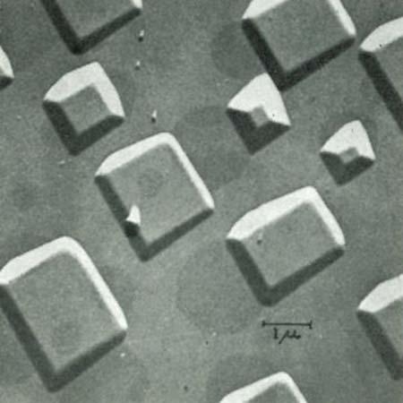
1.2TheMBEProcess AsfarasIamaware,thefirststudiesofgrowth,bywhatwenowcallMBE,wereperformedatPlesseyLabsinCaswellbyBruceJoyceandco-workers.TheygrewSifilms frommolecularbeamsofsilaneonaheatedSisubstrateunderUHVconditionsandthe resultingsampleswerestudiedbyRogerBookeratCambridgeUniversityusingtransmissionelectronmicroscopy(TEM).Thisstudywasconcernedwiththenucleationprocess itselfandverylowgrowthrateswereusedinordertoseparatereactionsonthesurface fromthoseinthegasphase,hencetheneedforcollision-freemolecularbeams.Thiswork waspublishedinaseriesofpapersfrom1966onwards[5–7]andwassummarisedina reviewarticlebyBruceJoycein1968[8].Theequipmentusedforthisstudyhadmanyof theattributesofamodernMBEsystem(havingcollimated,collision-free,molecularbeams ofsilaneimpingingonaheatedSisubstrate)andtookplaceunderUHVconditions;the pressureduringgrowthinthereactionchamberwas ∼3 × 10 9 Torr.Thegrowthrateswere smallcomparedtomodernpractiseandnoin-situcharacterisationwasinvolved,butinall otherrespectsthiscouldbeconsideredtobethefirststudyoftheMBEgrowthprocess.A resultfromthisstudyisshowninFigure1.1,whereitisclearthatSigrowsepitaxiallyon
Figure1.1 MBEdepositionofSifromsilaneonaheatedSisubstrateunderUHV conditions[8].
theheatedSisubstratebydecompositionfromthemolecularbeamofsilane[8],inother wordsbyMBE.
FollowingthisinitialworkonSi,whatfollowedwastheuseofMBEtogrowcompound semiconductors,mainlyIII–VsandtoalesserextentII–VIs,motivatedinpartbythe desiretoproducesemiconductorlasers.Theinitialworkonlaserswascarriedoutusing LPE(forthoseinterestedinthedevelopmentofsolid-statelasers,seetheexcellentbook onthestoryofsemiconductors[9]),butitsoonbecameapparentthatMBEcouldproduce equivalentorbetterresults.WhatfollowedwasthedevelopmentofMBEformany practicaldeviceapplications,includinglasers,transistors,andsoon.
ShortlyaftertheworkatPlesseycamethepioneeringworkatBellLabsbyJohnArthur andco-workers,whostudiedtheinteractionofmolecularbeamsofgalliumandarsenicon aheatedGaAssubstrateusingin-situmassspectrometry[10].Thiswasfollowedbyastudy ofthegrowthofGaAs,GaPandGaAsPbywhathetermedmolecularbeamdeposition[11]. Inhissystemthesourcesweresurroundedbyaliquidnitrogen-cooledshroudandin-situ massspectrometry,Augerelectronspectroscopy(AES)andlow-energyelectrondiffraction(LEED)wereusedforin-situanalysis.Thesystemalsohadprovisionforcleaningthe substratepriortogrowthusinganargoniongun.Themassspectrometercouldberotatedto enableittomeasureeitherthebeamsfromtheKnudsencellsorthespeciesdesorbingfrom thesurface.FromthisstudyitbecameclearthatforIII–Vsthegrowthrateiscontrolledby thearrivalrateofthegroupIIIspecies,providingthereisanexcessofthegroupVspecies. ItalsoshowedthattherelativestickingcoefficientsforAsandPareverydifferent.
ShortlyafterArthur’sworkatBellLabs,AlChojoinedMortonB.Panish’sgroupand embarkedonhispioneeringstudyofMBE.Aseveryoneknows,hemadeoutstanding contributionstobothunderstandingtheMBEprocessanditspracticalapplicationfor devices.Hissystemhadareflectionhigh-energyelectrondiffraction(RHEED)system forsurfaceanalysis,anargoniongunforsurfacecleaning,acylindricalmirroranalysis Augersystemforsurfacecompositionandagainthecellsweremountedwithinaliquid nitrogen-cooledshroud.ThechangefromLEEDtoRHEEDwascrucialandenabled real-timesurfaceanalysis,whichhasbecomethede-factostandardinallmodernMBE systems.IwilldiscussAlCho’smanycontributionstothegrowthofstructuresfor low-dimensionalstructuresanddevicesbelow,buthereIwishtopointoutsomeofhis criticalcontributionstounderstandingtheMBEprocess.Oneofhismostimportant contributionswastoshow,usingRHEED,thatforboththe(111)[12]and(001)[13] surfacesaclearcorrelationexistsbetweenthesurfacestructureweobserveandboththe III–Vratioandsubstratetemperature.Thesecondpaper[13]establishedthefactthat underAs-richconditionsonthe(001)surfaceweseeac(2 × 8)RHEEDpattern,which becomesac(8 × 2)patternunderGa-richconditions;inbetweenwealsoseeother6× patterns.Thiscrucialobservationenabledotherstofollowtheprocessandestablishthe optimumIII–Vratioandsubstratetemperatureforgrowth.In1971healsopublished apapershowinghowtheRHEEDpatterndevelopsduringgrowthfromdiffusespots tostreaksandatthesametimethesurfacegoesfromroughtosmooth[14].Thiswork wasdonelongbeforeatomicresolutionofthesurfacebyatomicforcemicroscopy (AFM)becameavailableandsothemythdevelopedthatstreakyRHEEDpatterns correspondtoatomicallyflatsurfaces;thishasbecomesoingrainedintheliterature thatitisstillstatedasgospeltoday!AlChoneversaidthatandweknowfromfirst principlesthatRHEEDstreakscomefromdisorderonthesurfaceandthatanatomically
smoothsurfacesuchastheSi(7 × 7)reconstructionwillshowsharpspotsintheRHEED pattern[15].
InparallelwiththeworkatBellLabs,theIBMgroupalsostudiedthegrowthofGaAs byMBEusingRHEED.Theyshowedhowthevarioussurfacereconstructionsrelatedto theAs2 :Garatioandsubstratetemperature[16].Inthatpapertheymakethestatementthat ‘ThestreakedRHEEDpatternindicatessmoothnessonanatomicscale’,whichisperhaps theoriginofthemythsurroundingRHEEDstreaks.Thispaperalsomentionstheuseof acomputertocontroltheMBEprocess,usingdatafromthein-situmassspectrometer measurements.
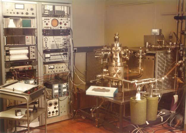
ShortlyafterthepioneeringworkatPlessey,BruceJoyceandJimNeavemovedto Mullards(laterPhilips)ResearchLaboratoriesatRedhilltoworkontheSi–SiO2 interface.Ijoinedthemin1969todoelectronmicroscopy,butthisprovedimpossibledueto lackofequipment.AtthesametimethereweredifficultieswiththeVPEprocessandso collectivelywesetouttostudythegrowthofGaAsbywhatbecameknownasmodulatedbeammassspectrometry(MBMS)(seeFigure1.2).Oursystemwassimilartothat atBell,buthadthemassspectrometermountedinaliquidnitrogen-cooledcryopanelto improvethesignal-to-noiseratio.WealsousedperiodicmodulationandFouriertransform techniquestoextracttheinformation,whichincludedmeasurementsofsurfacelifetime [17].WefirstusedthisequipmenttostudytheevaporationofGaAsunderequilibriumand non-equilibriumconditionsaspartofaPhDprogramme[18].Theresultswereessentially identicaltothosepreviouslyreportedbyJohnArthur[19],whichgaveusconfidencein ournewapproach.InaseriesofpaperswethenstudiedthegrowthofGaAsusingAs4 [20]andAs2 [21],beforestudyingalloyswithmixedgroupIII[22]andmixedgroupV
Figure1.2 ThesystemusedatMullards/Philipsformodulatedbeammassspectrometry measurements.