Green energy: solar energy, photovoltaics, and smart cities suman lata tripathi all chapter instant
Energy: Solar Energy, Photovoltaics, and
Visit to download the full and correct content document: https://ebookmass.com/product/green-energy-solar-energy-photovoltaics-and-smart-c ities-suman-lata-tripathi/
More products digital (pdf, epub, mobi) instant download maybe you interests ...
Digital VLSI Design and Simulation with Verilog Suman Lata Tripathi
For more information about Scrivener publications please visit www.scrivenerpublishing.com.
All rights reserved. No part of this publication may be reproduced, stored in a retrieval system, or transmitted, in any form or by any means, electronic, mechanical, photocopying, recording, or otherwise, except as permitted by law. Advice on how to obtain permission to reuse material from this title is available at http://www.wiley.com/go/permissions.
Wiley Global Headquarters
111 River Street, Hoboken, NJ 07030, USA
For details of our global editorial offices, customer services, and more information about Wiley products visit us at www.wiley.com.
Limit of Liability/Disclaimer of Warranty
While the publisher and authors have used their best efforts in preparing this work, they make no representations or warranties with respect to the accuracy or completeness of the contents of this work and specifically disclaim all warranties, including without limitation any implied warranties of merchantability or fitness for a particular purpose. No warranty may be created or extended by sales representatives, written sales materials, or promotional statements for this work. The fact that an organization, website, or product is referred to in this work as a citation and/or potential source of further information does not mean that the publisher and authors endorse the information or services the organization, website, or product may provide or recommendations it may make. This work is sold with the understanding that the publisher is not engaged in rendering professional services. The advice and strategies contained herein may not be suitable for your situation. You should consult with a specialist where appropriate. Neither the publisher nor authors shall be liable for any loss of profit or any other commercial damages, including but not limited to special, incidental, consequential, or other damages. Further, readers should be aware that websites listed in this work may have changed or disappeared between when this work was written and when it is read.
Library of Congress Cataloging-in-Publication Data
ISBN 978-1-119-76076-4
Cover image: Background - Suriya Siritam | Dreamstime.com, Graphic - Alberto Masnovo | Dreamstime.com
Cover design by Kris Hackerott
Set in size of 11pt and Minion Pro by Manila Typesetting Company, Makati, Philippines
USA
3.5
2.6.2
3.4.5
3.5.1
3.6.1
3.6.1.1
5.4.2
5.4.2.1
5.6
6.1
6.2.3
Saeed
7.1
6.3.3.1
6.3.3.2
7.2.1.1
7.2.1.5
7.2.1.6
7.2.2
7.2.3
7.2.4
7.2.5
7.2.6
7.3.1.1
7.3.1.2
7.3.1.3
7.3.1.4
7.3.2
7.3.3
7.3.4
Tohid Taghiloo, Kazem Varesi and Sanjeevikumar Padmanaban
Khurana and Sheela Tiwari
14 Theoretical Analysis
Mohamed G. Hussien and Sanjeevikumar Padmanaban
Dushyant Kumar Singh, Ashish Kumar Singh and Himani Jerath
16 Assessment of Economic and Environmental Impacts
Sunday O. Oyedepo, Emmanuel G. Anifowose, Elizabeth O. Obembe, Joseph O. Dirisu, Shoaib Khanmohamadi, Kilanko O., Babalola P.O., Ohunakin O.S., Leramo R.O. and Olawole O.C.
16.3.3
16.3.4
16.3.1.1
16.3.1.2
16.3.1.3
16.3.1.5
16.3.4.1
16.3.4.2
17 A Solar Energy–Based Multi-Level Inverter Structure
Fatemeh Esmaeili, Kazem Varesi and Sanjeevikumar Padmanaban
18.6
18.9
18.11
18.12
18.13
19 A Developed Large Boosting Factor DC-DC
Saeid Deliri Khatoonabad, Kazem Varesi and Sanjeevikumar Padmanaban
20.1
20.3
Preface
Green energy technology has not only given a concept of clean energy but also reduces dependency on fossil fuel for electricity generation through smart power electronics integration. Also, endless resources have more potential to cope with the requirements of smart building and smart city concept. The power electronics in a smart and intelligent approach can lead to highly efficient energy systems supporting the increasing demand for eco-friendly energy systems. The objective of this edition is to provide a broad view of the fundamental concepts and development process of green energy technology in a concise way for fast and easy understanding. This book provides information regarding almost all aspects to make it highly beneficial for all students, researchers and teachers of this field. Fundamental principles of green energy systems with AI and machine learning techniques are discussed herein in a clear and detailed manner with an explanatory diagram wherever necessary. The technological trends and latest developments based on green energy systems and applications are the major focus of the book. All the chapters are illustrated in simple language which will facilitate readability of the chapters.
Chapter Organization
This book is organized into 20 chapters.
Chapter 1 discusses the crystalline silicon solar cell (c-Si)–based technology that has been recognized as the environment-friendly viable solution to replace traditional energy sources for power generation. The chapter mainly elaborates the three basic c-Si solar cell configurations that are monofacial, bifacial and back-contacted solar cell configurations.
Chapter 2 is mainly focused on p-type mono-Si-PERC and n-type c-Si based TOPCon solar cell with enhanced efficiency. The use of HJ-TF cells, the Cu2O, InGaN, CuInS2, and InP fabrics are also explored for solar cell developments.
Chapter 3 summarizes the recent advancement made in the fabrication and manufacturing process for commercialization of PSC in the photovoltaic (PV) market and also various possible techniques used to improve their physical properties, and overcome hurdles and challenges while fabricating perovskite films.
Chapter 4 presents a short yet comprehensive survey on the metaheuristic approaches to the parameter assessment of solar photovoltaic systems modelled by different diode models.
Chapter 5 describes the review and challenge in solar PV cell design and implementation. Furthermore, it outlines the existing PV systems, the structure of different PV panels, MPPT, and the solid-state converter topologies.
Chapter 6 compares the developed method with its traditional counterpart, and the results of the experiment show that the new model performs better in terms of computational efficiency, compression gain, and SOH estimation accuracy.
Chapter 7 presents a detailed discussion on power quality (PQ) disturbances that cause rigorous issues in smart grids and industries. This mainly covers event-driven processing, analysis and machine learning for successful and efficient detection of PQ disturbances.
Chapter 8 is intended to provide information about the structural, optical, dielectric and conductivity with the help of compositional modification at Sr-site of Sr2SnO4 by homovalent (Ba2+) and hetrovalent (La3+).
Chapter 9 focuses on the detailed modelling of a solar photovoltaic (PV) panel. Here, a single-diode four-parameter model is also described that can be used for all panels in general.
Chapter 10 explores a stepped DC link converter for solar power that is focused for configurations of BCMLI, CDCLHBI and BCDCLHBI and synthesizing seven-level AC power output.
Chapter 11 derived a new modified double-diode model equation and on the basis of that formed a new objective function for MDDM. The HHO algorithm was used to estimate all the eight parameters of the system for different types of commercially available PV modules.
Chapter 12 describes a switched-inductor switched-capacitor-based large-gain DC-DC converter with low voltage stress on its switches/diodes.
Chapter 13 envisages presenting the stability concerns and issues associated with microgrids along with a state-of-the-art review of the techniques employed for improving stability of microgrids working in either islanded or grid-connected mode.
Chapter 14 deals with three-phase current ripples, and also the torque ripple of a surface-mounted permanent magnet synchronous motor
Preface xxi
(SPMSM) was completely analysed and minimized based on the variable switching frequency PWM (VSFPWM) method.
Chapter 15 discuss the implementation of Internet of Things (IoT) in the Smart Home, which plays a major role in making the things automatic and also saves a lot of energy.
Chapter 16 deals with the assessment of the economic and environmental impacts of energy conservation strategies in a university campus.
Chapter 17 suggests a novel double-source basic unit for cascaded MLIs that can produce seven output voltage steps with Trinary magnitude of DC supplies. The suggested structure can operate as symmetric or asymmetric MLI.
Chapter 18 presents the designing procedure of conventional and the vector control, Proportional Integral (PI) controller and analyzes the performance characteristics of DFIG connected to the Grid Systems.
Chapter 19 describes the combination of conventional SEPIC and quadratic boost converters with a boosting stage, which increases the boosting factor of converter. The continuous input-current as well as large boosting capability make the proposed topology applicable for Photovoltaic (PV) applications.
Chapter 20 proposes two novel basic configurations for switchedcapacitor-based 13- and 17-level inverters, with high step-up capability and self-voltage balancing of capacitors.
1
Fabrication and Manufacturing Process of Solar Cell: Part I
S. Dwivedi
S.S. Jain Subodh P.G. (Autonomous) College, Jaipur, India
Abstract
Crystalline silicon solar cell (c-Si) based technology has been recognized as the only environment-friendly viable solution to replace traditional energy sources for power generation. It is a cost-effective, renewable and long-term sustainable energy source. The Si-based technology has a market growth of almost 20-30% and is projected to attain an energy share of ~100 giga watt (GW) per year in the current fiscal year, 2020. There have been constant efforts in reducing manufacturing cost of solar panel technology, which is about three-four times higher in comparison to traditional carbon-based fuels. In the manufacturing domain, fabrication of three basic c-Si solar cell configurations can be utilized, which are differentiated in the manner of generation of electron-hole (E-H) pairs on exposure to sunlight. The generation of electricity by impinging light on a semiconductor material requires production of electrons and holes such that electrons in the valence band become free and jump to the conduction band by absorbing energy. Thus, jumping of highly energetic electrons to different material generates an electromotive force (EMF) converting light energy into electrical signals. This is known as the photovoltaic (PV) effect.
This chapter is an effort to outline fabrication processes and manufacturing methodologies for commercial production of large area PV modules as an alternative green source of energy.
Keywords: Solar cell, photovoltaics, p-n junction, photovoltaic panels, crystalline silicon solar cell, renewable energy, physics of solar cell, fabrication of solar cell
There has always been a surge to discover newer sources of energy which can be effective alternatives for the orthodox sources of energy, such as, petrol, kerosene, wind energy, thermal power generators [1,2]. In this quest, the sun is a natural huge source of renewable green energy. It is noteworthy that the terrestrial soil is exposed to an enormous amount of solar energy as large as about ten thousand times of all the energy used around the globe. The terrestrial hemisphere facing the sun receives power in excess of 50,000 terawatt (TW) in each instance, which makes reception of an enormous amount of energy possible [3]. Photovoltaics (PV) technology is a technology that relies on this infinite source of sunlight and possesses inherent qualities of highly reduced service costs since the sun provides free energy, reliability, noiseless, minimum maintenance costs and readily installation features [4, 5].
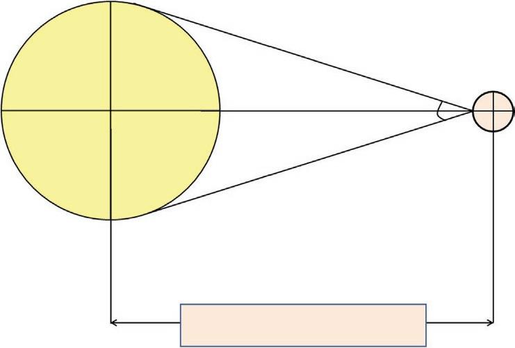
As a matter of fact, thermonuclear fusion reactions happen non-stop at a temperature of millions of degrees to generate huge energy in the form of electromagnetic radiation of sunlight [5,6]. The outer layer of the earth’s atmosphere receives partial energy of the total energy from the sun with a solar constant or an average irradiance of approximately 1367 Wm-2 with a variation of ±3% [8]. This value of solar constant is dependent on the earthto-sun distance and on the solar activity. The solar constant is defined as the intensity of solar electromagnetic radiation impinging on a unit surface area and is expressed in units of kWm-2 and is equal to the integral of the power of the individual frequencies in the spectrum of solar radiation. The geometry of the sun-to-earth distance is displayed in Figure 1.1 given below.
Solar irradiation is the integral of solar irradiance over a particular period of time depicted by kWhm-2 and the radiation falling on the surface of the earth is actually diffuse radiation [8]. Diffuse radiation is that part of light radiation striking the surface from whole of the sky, while other radiations are the part reflected from the ground, and by surrounding atmosphere. Different types of radiation received by a solar panel [9] are displayed in Figure 1.2 as shown below.
1.1.1 Introduction to Si-Based Fabrication Technology
Photovoltaics technology is a green method of energy production which is based on fabrication and manufacturing of solar cells on platform of Si wafers [9]. In this regard, it is mandatory to know about the Si wafers. So the silicon and its geometry as an integral component of the solar cell technology will be discussed first.
Fabrication and Manufacturing Process of Solar Cell: Part I 3
Diameter of Sun = ~1.39 × 10⁶ km
Diameter of Ear th = 12,742 km
Solar Constant = 1367Wm–2 ± 3%
Distance between earth & sun = ~1.49 × 10⁸ km
Figure 1.1 The above schematic shows the sun-earth geometry portraying distance between the two celestial objects, diameters and the value of solar constant.
Figure 1.2 The above figure portrays different radiations occurring from the sun which consists of direct, diffuse and reflected radiations.
1.1.2 Introduction to Si Wafer
Silicon is a member of group 14 in the periodic table and is tetravalent metalloid, semiconductor and brittle crystalline solid [10-12]. In 1906, a silicon radio crystal detector was developed as the first silicon-based semiconductor device by Greenleaf Whittier Pickard [13]. Russell Ohl discovered the nonlinear semiconductor devices, p-n junction, and photovoltaic effect in the metalloid Si in 1940 [14]. In 1941, during the Second World War, radar microwave detectors were invented by developing techniques for production of high quality germanium (Ge) and Si crystals [15]. William Shockley proposed a field-effect amplifier based on Ge and Si in 1947, but could not demonstrate the prototype practically [16]. John Bardeen and Walter Brattain built the first working device, point-contact transistor, in 1947 under the direction of Shockley only [17]. The first Si-based junction transistor was fabricated by the physical chemist Morris Tanenbaum in 1954 at Bell Labs [18]. At Bell Labs in 1954, Carl Frosch and Lincoln Derick found out by accident that it is possible to grow silicon-di-oxide (SiO2) on Si wafers [19]. Later on, in 1958, they discovered that this as-grown SiO2 could be used to mask Si surfaces during diffusion processes [19].
Si atom has fourteen electrons with electronic configuration 2,8,4 [1s2, 2s2, 2p6, 3s2, 3p2] specifying that the number of valence electrons is 4 [10,11]. These valence electrons occupy the 3s orbital and two 3p orbitals. In order to complete its octet and attain the stable noble gas configuration of Argon (Ar), it can combine with other elements to form SiX4 derivatives by forming sp3 hybrid orbitals. In this case, the central Si atom taking part in the bonding with other element shares an electron pair with each of the four atoms of the bonding element.
Si and Ge crystallize in a diamond-type cubic lattice structure which has the space-lattice of face-centered cubic (fcc) [20, 21]. The atomic positions in the diamond-type cubic lattice projected on a cubic platform are shown in Figure 1.3. In a space-lattice of fcc-type, two identical atoms at 000 and 1 4 1 4 1 4 form the primitive basis and are associated with each point of the fcc lattice. In the above picturesque, fractions are the heights over and above the base in units of a cube edge. In that case, points at 0 and 1 2 lie on the fcc lattice, while those at 1 4 and 3 4 lie on the similar fcc lattice but are displaced along the line of body diagonal by a magnitude of ¼ of its length. It is a known fact that the unit cube of fcc lattice consists of 4 lattice points. As a result, diamond-type cubic lattice contains 2 × 4 = 8 atoms. The diamond-type fcc lattice in Si displays tetrahedral bonding characteristics [20, 21].
Si is tetravalent and can be made p-type by adding dopants of boron (B), aluminium (Al) & gallium (Ga), and addition of antimony (Sb), phosphorous (P) & arsenic (As) generates n-type semiconductor material [10,11,20,21]. B and Ga possess only three valence electrons and when they are mixed into the Si lattice, deficiency of an electron is created which is termed as positively charged “vacancy” or “hole”. Holes take part in conduction accepting an electron from the neighbour and transitioning over the atoms. For making Si an n-type semiconductor, Sb, P and As are added into the Si lattice in small quantities each having five valence electrons, which creates an extra electron into the lattice. The availability of these free electrons as a whole in the material creates a net flow of negatively charged carriers to constitute current. Thus, addition of small amounts of either of two types of foreign atoms changes Si crystal into a medium-type of conductor, which is a semiconductor. Joining of two types of semiconducting materials constitutes a device entailed as nonlinear semiconductor diode [10,11,20-22]. Figure 1.4 shows a similar picture to portray the doping of two types of foreign atoms in Si lattice.
1.1.3 Introduction to Diode Physics
When p-type and n-type junctions are combined to form p-n junctions, they possess a characteristic called rectification [23-26]. Rectification is a
Figure 1.3 Schematic to show atomic positions in diamond-type cubic lattice.
Figure 1.4 Figure showing the doping of two types of foreign atoms of B (p-type) and P (n-type) in Si to form semiconductor material with better conductivities.
property to allow flow of current easily in one direction only [28,29]. In the case of p-type material, the Fermi level (EF) is near the valence band edge and is close to conduction band edge in n-type material as shown in Figure 1.5. In p-type configuration, holes are the majority carriers, while electrons are minority carriers. Just the opposite happens in case of n-type materials in which electrons are majority carriers and holes are minority carriers. Upon joining, large carrier concentration gradients happen at the junction to cause carrier diffusion. Majority holes from the p-type are transported by diffusion into the n-type semiconductor, while majority
Figure 1.5 Two semiconductor blocks of p-type and n-type before the formation of junction and also showing position of Fermi level (EF) in the corresponding dopes semiconductor material.