Where can buy Chiplet design and heterogeneous integration packaging john h. lau ebook with cheap pr
Chiplet Design and Heterogeneous Integration Packaging John H. Lau
Visit to download the full and correct content document: https://ebookmass.com/product/chiplet-design-and-heterogeneous-integration-packag ing-john-h-lau/
More products digital (pdf, epub, mobi) instant download maybe you interests ...
Modeling, Analysis, Design and Tests for Electronics
This work is subject to copyright. All rights are solely and exclusively licensed by the Publisher, whether the whole or part of the material is concerned, specifically the rights of translation, reprinting, reuse of illustrations, recitation, broadcasting, reproduction on microfilms or in any other physical way, and transmission or information storage and retrieval, electronic adaptation, computer software, or by similar or dissimilar methodology now known or hereafter developed.
The use of general descriptive names, registered names, trademarks, service marks, etc. in this publication does not imply, even in the absence of a specific statement, that such names are exempt from the relevant protective laws and regulations and therefore free for general use.
The publisher, the authors, and the editors are safe to assume that the advice and information in this book are believed to be true and accurate at the date of publication. Neither the publisher nor the authors or the editors give a warranty, expressed or implied, with respect to the material contained herein or for any errors or omissions that may have been made. The publisher remains neutral with regard to jurisdictional claims in published maps and institutional affiliations.
This Springer imprint is published by the registered company Springer Nature Singapore Pte Ltd. The registered company address is: 152 Beach Road, #21-01/04 Gateway East, Singapore 189721, Singapore
Preface
There are at least five different chiplet design and heterogeneous integration packaging, namely (1) chip partition and heterogeneous integration (driven by cost and technology optimization), (2) chip split and heterogeneous integration (driven by cost and semiconductor manufacturing yield), (3) multiple system and heterogeneous integration with thin-film layer directly on top of a build-up package substrate (2.1D IC integration), (4) multiple system and heterogeneous integration with throughsilicon via (TSV)-less interposer (2.3D IC integration), and (5) multiple system and heterogeneous integration with TSV interposers (2.5D and 3D IC integration).
In chip partition and heterogeneous integration, the system-on-chips (SoCs), such as the logic and I/Os, are partitioned into functions: logic and I/O. These chiplets can be stacked (integrated) by the front-end chip-on-wafer (CoW) or wafer-on-wafer (WoW) methods and then assembled (integrated) on the same substrate of a single package by using the heterogeneous integration technique. It should be emphasized that the front-end chiplets’ integration can yield a smaller package area and better electrical performance but is optional.
In chip split and heterogeneous integration, the SoC, such as logic, is split into smaller chiplets, such as logic1, logic2, and logic3. These chiplets can be stacked (integrated) by the front-end CoW or WoW methods and then assembled on the same substrate of a single package by using the heterogeneous integration technique. Again, the front-end integration of chiplets is optional.
In multiple system and heterogeneous integration with thin-film layers directly on top of the build-up package substrate, the SoC such as the central processing unit (CPU), logic, and high-bandwidth memory (HBM) are supported by a buildup package substrate with thin-film layers. This is driven by performance and form factor and for high-density and high-performance applications.
In multiple system and heterogeneous integration with TSV-less interposers, the SoC such as the CPU, logic, and HBM are supported by a fine metal line width (L) and spacing (S) redistribution-layer (RDL)-substrate (organic interposer) and then on a build-up package substrate. This is driven by performance and form factor and for high density and performance applications.
In multiple system and heterogeneous integration with TSV-interposers, the SoC such as the CPU, logic, and HBM are supported by a passive (2.5D) or active (3D) TSV-interposer and then on a build-up package substrate. This is driven by performance and form factor and for extremely high-density and high-performance applications.
For the next few years, we will see more implementations of a higher level of chiplet designs and heterogeneous integration packaging, whether it is for yield, cost, time-to-market, performance, form factor, or power consumption. Unfortunately, for most of the practicing engineers and managers, as well as scientists and researchers, these chiplet design and heterogeneous integration packaging methods are not well understood. Thus, there is an urgent need, both in industry and research institute, to create a comprehensive book on the current state of knowledge of these chiplet design and heterogeneous integration packaging technologies. This book is written so that readers can quickly learn about the basics of problem-solving methods and understand the trade-offs inherent in making system-level decisions.
There are six chapters in this book, namely (1) State-of-the-Art of Advanced Packaging, (2) Chip Partition Heterogeneous Integration and Chip Split Heterogeneous Integration, (3) Multiple System and Heterogeneous Integration with TSVInterposers, (4) Multiple System and Heterogeneous Integration with TSV-Less Interposers, (5) Chiplets Lateral Communications, and (6) Cu-Cu Hybrid Bonding.
Chapter 1 presents the recent advances and trends in semiconductor advanced packaging. The kinds of advanced packaging are ranked based on their interconnect density and electrical performance and are grouped into 2D, 2.1D, 2.3D, 2.5D, and 3D IC integration, which will be presented and discussed. Fan-in packaging, such as the six-sided molded wafer-level chip-scale package (WLCSP) and its comparison with the ordinary WLCSP are presented. Fan-out packaging such as the chip-first with die face-up, chip-first with die face-down, and chip-last and their difference will be provided.
Chapter 2 presents the chiplet design and heterogeneous integration packaging, especially (a) chip partition and heterogeneous integration and (b) chip split and heterogeneous integration. Emphasis is placed on their advantages and disadvantages, design, materials, process, and examples. System-on-chip (SoC) and Defense Advanced Research Projects Agency’s (DARPA) efforts in chiplet heterogeneous integration will be briefly mentioned first.
Chapter 3 details the recent advances in multiple system and heterogeneous integration with passive/active TSV interposers. Emphasis is placed on the definition, kinds, advantages and disadvantages, challenges (opportunities), and many examples of multiple system and heterogeneous integration with TSV-interposer. Also, some recommendations will be provided.
Chapter 4 presents the recent advances in multiple system and heterogeneous integration with TSV-less interposers (2.3D IC integration). Some of the challenges (opportunities) of 2.3D IC integration (organic interposer) will also be presented. Some recommendations of 2.3D IC integration will be provided. Finally, characterization of low-loss dielectric materials for organic interposer will be presented. Some
fundamentals and recent advances in fan-out technology will be briefly mentioned first.
Chapter 5 presents the lateral (horizontal) communications (bridges) between chiplets. Various kinds of bridges such as the ridge bridges embedded in build-up package substrate and those embedded in fan-out epoxy molding compound, and the flexible bridges will be presented. UCIe will also be briefly mentioned.
Chapter 6 presents the recent advances and trends in Cu-Cu hybrid bonding. Emphasis is placed on the definition, kinds, advantages and disadvantages, challenges (opportunities), and examples of Cu-Cu bumpless hybrid bonding. Also, some recommendations will be provided. The direct Cu-Cu thermocompression bonding (TCB) and direct SiO2 -SiO2 TCB will be briefly mentioned first.
For whom is this book intended? Undoubtedly it will be of great interest to three groups of specialists: (1) those who are active or intend to become active in research and development of chiplet design and heterogeneous integration packaging, (2) those who have encountered practical chiplet design and heterogeneous integration packaging problems and wish to understand and learn more methods for solving such problems; and (3) those who have to choose a reliable, creative, high performance, high density, low power consumption, and cost-effective technique for their products. This book can also be used as a text for college and graduate students who have the potential to become our future leaders, scientists, and engineers in the electronics and optoelectronics industry.
I hope that this book will serve as a valuable reference source for all those faced with the challenging problems created by the ever-increasing interest in chiplet design and heterogeneous integration packaging. I also hope that it will aid in stimulating further research and development on key enabling technologies and more sound applications to chiplet design and heterogeneous integration packaging products. The organizations that learn how to design and manufacture chiplet design and heterogeneous integration packaging in their semiconductor packaging systems have the potential to make major advances in the electronics and optoelectronics industry, and to gain great benefits in cost, performance, functionality, density, power, bandwidth, quality, size, and weight. It is my hope that the information presented in this book may assist in removing roadblocks, avoiding unnecessary false starts, and accelerating design, materials, process, and manufacturing development of chiplet design and heterogeneous integration packaging.
Palo Alto, CA, USA
John H. Lau
Acknowledgments
Development and preparation of semiconductor advanced packaging were facilitated by the efforts of a number of dedicated people. I would like to thank them all, with special mention of Kumar Boominathan and Satish Ambikanithi, Springer Nature Scientific Publishing Services (P) Ltd., for their unswerving support and advocacy. My special thanks go to Ms. Jasmine Dou, Springer Singapore, who made my dream of this book come true by effectively sponsoring the project and solving many problems that arose during the book’s preparation. It has been a great pleasure and fruitful experience to work with all of them in transferring my messy manuscripts into a very attractive printed book.
The material in this book clearly has been derived from many sources, including individuals, companies, and organizations, and I have attempted to acknowledge by citations in the appropriate parts of the book the assistance that I have been given. It would be quite impossible for me to express my thanks to everyone concerned for their cooperation in producing this book, but I would like to extend due gratitude. Also, I would like to thank several professional societies and publishers for permitting me to reproduce some of their illustrations and information in this book, including the American Society of Mechanical Engineers (ASME) conference proceedings (e.g., International Intersociety Electronic Packaging Conference) and transactions (e.g., Journal of Electronic Packaging), the Institute of Electrical and Electronics Engineers (IEEE) conference proceedings (e.g., Electronic Components and Technology Conference and Electronics Packaging and Technology Conference) and transactions (e.g., Components, Packaging, and Manufacturing Technologies), and the International Microelectronics and Packaging Society (IMAPS) conference proceedings (e.g., International Symposium on Microelectronics), and transactions (e.g., International Journal of Microcircuits and Electronic Packaging).
I would like to thank my former employers, ASM (HK), Industrial Technology Research Institute (ITRI), the Hong Kong University of Science and Technology (HKUST), the Institute of Microelectronics (IME), Agilent, and HP, for providing me with excellent working environments that have nurtured me as a human being, fulfilled my need for job satisfaction, and enhanced my professional reputation. Also,
I would like to thank Dr. Don Rice (HP), Dr. Steve Erasmus (Agilent), Prof. DimLee Kwong (IME), Prof. Ricky Lee (HKUST), Dr. Ian Yi-Jen Chan (ITRI), and Mr. Lee Wai Kwong (ASM) for their kindness and friendship while I was at their organizations. Furthermore, I would like to thank Mr. Tzyy-Jang Tseng (Chairman of Unimicron Technology Corporation) for his trust, respect, and support of my work at Unimicron. Finally, I would like to thank the following colleagues for their stimulating discussions and significant contributions to this book: T. C. Chai, L. Chang, H. Chang, P. Chang, Y. Chang, Y. Chao, E. Charn, C. Chen, G. Chen, J. Chen, S. Chen, R. Cheng, Y. Cheng, C. Chien, H. Chien, R. Chou, J. Cline, Y. Fang, H. Fu, Z. Hsiao, Y. Hsin, Y. Hsu, J. Huang, Y. Huang, M. Kao, N. Khan, C. T. Ko, V. Kripesh, T. Ku, C.-K. Lee, P. Lee, T. Lee, V. Lee, Y. Lee, M. Li, E. Liao, L. Liao, S. Lim, B. Lin, C. Lin, E. Lin, N. Liu, W. Lo, M. Ma, R. Nagarajan, C. Peng, P. Peng, V. Rao, K. Saito, R. Tain, W. Tsai, T. Tseng, P.-J. Tzeng, J. Wang, H. We, C. Wu, S. Wu, T. Xia, C. Yang, K. Yang, C. Zhan, and X. Zhang. Definitely, I would like to thank my eminent colleagues (the enumeration of whom would not be practical here) at Unimicron, ASM, ITRI, HKUST, IME, Agilent, EPS, HP, and throughout the electronics industry for their useful help, strong support, and stimulating discussions. Working and socializing with them has been a privilege and an adventure. I learned a lot about life and chiplet design and heterogeneous integration packaging from them. Lastly, I would like to thank my daughter Judy and my wife Teresa for their love, consideration, and patience by allowing me to work peacefully on this book. Their simple belief that I am making a contribution to the electronics industry was a strong motivation for me. Thinking that Judy and her supportive husband (Bill) have been doing very well in the electronics industry and their two adorable kids (Allison and James) have been raising in a happy and loving environment, and Teresa and I are in good health, I want to thank God for His generous blessings.
Palo Alto, CA, USA
John H. Lau
3.1
3.2 Through-Silicon
3.2.1
3.2.2
3.2.3
3.2.4
3.3
3.4
3.5
3.7
3.5.1
3.5.2
3.7.5
3.7.6 NVidia/TSMC’s Multiple System and Heterogeneous Integration
3.7.7 TSMC’s Multiple System and Heterogeneous Integration with DTC
3.7.8 Samsung’s Multiple System and Heterogeneous Integration with Integrated Stack Capacitor (ISC)
3.7.9
3.7.10
3.7.11
3.7.12
3.7.13
3.7.14
3.7.15
3.7.16
3.7.17
3.7.18
3.7.19
3.7.20
3.7.21
3.7.22
3.10
4.4 2.3D
4.8
4.5.4
Fan-Out (Chip-Last or RDL-First)
5.4.2
5.5
5.5.1
5.5.2
5.5.3
5.6
5.9
5.9.1
5.9.2
6.3.2
6.4
6.5
6.6
6.7
6.8
6.7.2
About the Author
John H. Lau, Ph.D., P.E. was the CTO from July 2019 to July 2021 and has been a Senior Special Project Assistant since August 2021 of Unimicron in Taiwan. Prior to that, he was a Senior Technical Advisor at ASM Pacific Technology in Hong Kong for 5 years; a specialist of the Industrial Technology Research Institute in Taiwan for 5 years; a Visiting Professor at Hong Kong University of Science and Technology for 1 year; the Director of the Microsystems, Modules, and Components Laboratory at the Institute of Microelectronics in Singapore for 2 years; and a Senior Scientist/MTS at Hewlett-Packard Laboratory/Agilent in California for more than 25 years.
His professional competences are design, analysis, materials, process, manufacturing, qualification, reliability, testing, and thermal management of electronic, optoelectronic, LED, CIS, and MEMS components and systems, with emphases on solder mechanics and manufacturing, RoHS-compliant products, SMT, flip chip, fan-in and fan-out wafer/panel-level packaging, SiP, chiplet design and heterogeneous integration packaging, and TSV and other enabling technologies for 3D IC integration.
With more than 40 years of R&D and manufacturing experience, he has authored or coauthored more than 515 peer-reviewed articles (out of which 370 are the principal investigator), invented more than 40 issued or pending US patents (out of which 25 are the principal inventor), and given more than 320 lectures/workshops/keynotes worldwide. He has authored or coauthored 23 textbooks (all are the first author) on semiconductor advanced packaging, fan-out wafer-level packaging, 3D IC heterogeneous integration and packaging, TSV for 3D integration, advanced MEMS packaging, reliability of 2D and 3D IC interconnects, flip chip, WLP, MCM, areaarray packages, WLCSP, high-density PCB, SMT, DCA, TAB, lead-free materials, soldering, manufacturing, and solder joint reliability.
He earned a Ph.D. degree in theoretical and applied mechanics from the University of Illinois at Urbana–Champaign, an M.A.Sc. degree in structural engineering from the University of British Columbia, a second M.S. degree in engineering mechanics from the University of Wisconsin at Madison, and a third M.S. degree in management science from Fairleigh Dickinson University in New Jersey. He also has a B.E. degree in civil engineering from National Taiwan University. xxi
He has received many awards from the American Society of Mechanical Engineers (ASME), the Institute of Electrical and Electronics Engineers (IEEE), the Society of Manufacturing Engineers (SME), and other societies, including for the best IEEE/ECTC proceedings paper (1989), outstanding IEEE/EPTC paper (2009), best ASME transactions paper (Journal of Electronic Packaging, 2000), best IEEE transactions paper (CPMT, 2010), the ASME/EEP Outstanding Technical Achievement Award (1998), IEEE/CPMT Manufacturing Award (1994), IEEE/CPMT Outstanding Contribution Award (2000), IEEE/CPMT Outstanding Sustained Technical Contribution Award (2010), SME Total Excellence in Electronics Manufacturing Award (2001), Pan Wen Yuan Distinguished Research Award (2011), IEEE Meritorious Achievement in Continuing Education Award (2000), IEEE Components, Packaging, and Manufacturing Technology Field Award (2013), and ASME Worcester Reed Warner Medal (2015). He is an elected ASME fellow, IEEE fellow, and IMAPS fellow and has been actively participating in industry/academy/society meetings/conferences to contribute, learn, and share.
Chapter 1
State-Of-The-Art
of Advanced Packaging
1.1 Introduction
In this chapter, advanced packaging is defined. The kinds of advanced packaging are ranked based on their interconnect density and electrical performance, and are grouped into 2D, 2.1D, 2.3D, 2.5D, and 3D IC integration, which will be presented and discussed. Chiplet design and heterogeneous integration packaging provide alternatives to the system on chips (especially for advanced nodes) will be discussed. Different substrates, such as size, pin-count, and metal linewidth and spacing for advanced packaging, are examined. The lateral communication between chiplets, such as the silicon bridges embedded in organic build-up package substrate and fanout epoxy molding compound, as well as flexible bridges, will be presented. Fan-in packaging, such as the six-side molded wafer-level chip-scale package (WLCSP) and its comparison with the ordinary WLCSP, are presented. Fan-out packaging, such as the chip-first with die face-up, chip-first with die face-down, and chip-last and their difference, will be provided. Low-loss dielectric materials for high-speed and highfrequency applications in advanced packaging will be presented. Flip-chip assembly by mass reflow, thermocompression bonding, and bumpless hybrid bonding will be briefly mentioned first.
Semiconductor industry has identified five major growth engines (applications) [1, 2], namely: (1) mobile (such as smartphones, smartwatches, and wearables) and portable (such as notebooks and cameras); (2) high-performance computing (HPC), also known as supercomputing, which is able to process data and perform complex calculations at high speeds on a supercomputer; (3) autonomous vehicle (or selfdriving cars); (4) Internet of Things (IoT), such as smart factory and smart health; and (5) big data (for cloud computing) and instant data (for edge computing). There are many system-technology drivers, such as artificial intelligence (AI) and fifthgeneration (5G technology standard for broadband cellular networks), which are boosting the growth of these five semiconductor applications. Because of the drive of 5G and AI, the semiconductors’ speed increases, the interconnect density increases,
the pad pitch decreases, the chip size increases, and power dissipation increases. All these provide challenges (opportunities) to advanced packaging.
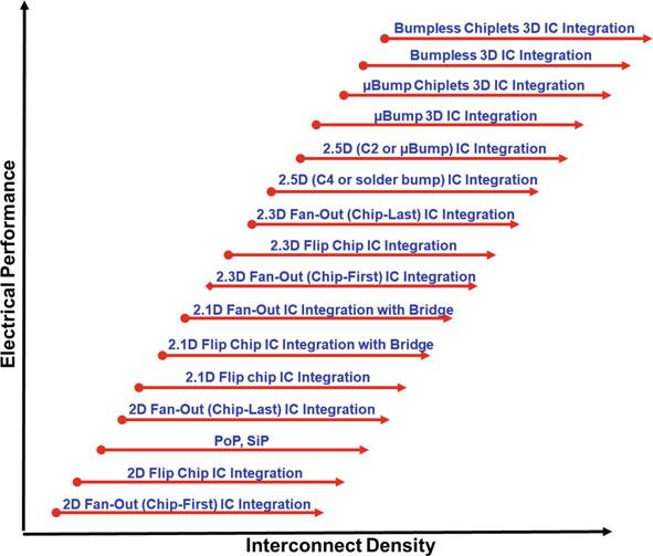
There are many advanced packaging technologies (to house the semiconductors), such as the 2D fan-out (chip-first) IC integration, 2D flip-chip IC integration, package on package (PoP), the system-in-package (SiP), 2D fan-out (chip-last) IC integration, 2.1D flip-chip IC integration, 2.1D flip-chip IC integration with bridges, 2.1D fan-out IC integration with bridges, 2.3D fan-out (chip-first) IC integration, 2.3D (organic substrate) IC integration, 2.3D fan-out (chip-last) IC integration, 2.5D (solder bump) IC integration, 2.5D [microbump (μbump)] IC integration, μbump 3D IC integration, μbump chiplets 3D IC integration, bumpless 3D IC integration, and bumpless chiplets 3D IC integration. Depending on applications, their electrical performance and interconnect density ranking are schematically shown in Fig. 1.1. Figure 1.2 shows the groups of packaging.
The simplest packaging method is directly attaching the semiconductor chip on a printed circuit board (PCB), such as chip-on-board (COB) or direct chip attach (DCA) [3–5], Fig. 1.3. Lead-frame packages, such as plastic quad flat pack (PQFP) and small outline integrated circuit (SOIC), are ordinary packages [6, 7]. Even plastic ball grid array (PBGA) [8] and flip-chip–chip-scale package (fcCSP) [9] for single chip (Fig. 1.4) are conventional packages [10]. In this book, advanced packaging is defined (see Fig. 1.2) as from the 2D IC integration with multichip on a package substrate or fan-out redistribution-layer (RDL) substrate. If the package substrate
Fig. 1.1 Advanced packaging ranking according to their density and performance
Semiconductors (Regular, SoC, Chiplets, etc.)
Substrate (Carrier)
Fig. 1.2 Groups of advanced packaging: 2D, 2.1D, 2.3D, 2.5D, and 3D IC integration
has thin-film layers on top, then it is called the 2.1D IC integration. If the package substrate or the fan-out epoxy molding compound (EMC) has embedded bridges, then it is called the 2.1D IC integration with bridges. If the multichips are supported by an inorganic/organic through-silicon via (TSV)-less interposer (substrate) and then attached on a package substrate, then it is called the 2.3D IC integration. If the multichips are supported by a passive TSV interposer and then attached to a package substrate, then it is called the 2.5D IC integration. If the multichips are supported by an active TSV interposer and then attached on a package substrate, then it is called the 3D IC integration. There is one exception, where one single chip on an active TSV interposer is also called 3D IC integration [11, 12].
In this chapter, the recent advances of 2D, 2.1D, 2.3D, 2.5D, and 3D IC integrations will be briefly discussed. Chiplet design and heterogenous integration packaging [13], fan-in [14] and fan-out [15] packaging, and low-loss dielectric materials for high-speed and high-frequency applications will also be presented. Flip-chip [4, 15] bumping and bonding/assembly will be briefly mentioned first.
Fig. 1.3 Direct chip attached on board
Solder Balls Solder Bumps
Lid
Solder Balls
Solder Bumps Solder Balls
Fig. 1.4 Flip-chip–chip-scale package (fcCSP)
1.2 Flip-Chip Bumping and Bonding/Assembly
1.2.1 Flip-Chip Bumping
There are many flip-chip bumps, such as Au bumps, Ni bumps, Cu studs, and solder bumps [5, 16]. Today, the controlled collapse chip connection (C4) bumps are the most used. For very high-density and fine-pitch, chip connection (C2) bumps are used. The C4 and C2 bumping processes have been presented in [17] and are systemically shown in Fig. 1.5a, b, respectively. One of the examples of the application of C4 and C2 bumps has been given by Amkor [see Fig. 1.5c]. In this book, C4 bumps can be any kind of solder, and C2 bumps consist of Cu pillar + any kind of solder caps, which is also called μbump. Because the solder volume is very small compared with the C4 bump, the surface tension of the C2 bump is not enough to perform the self-alignment. On the other hand, besides being able to handle finer pitch, C2 bumps also provide better thermal and electrical performances than C4 bumps, as shown in Table 1.1.
(a) C4 bump
(b) C2 bump
(c) Flip chips with C2 and C4 bumps
Table 1.1 C4 bumps versus C2 bumps: bump pitch and self-alignment
C4 bump (solder)
C2 bump (Cu pillar + solder cap)
(effective)
1.2.2 Flip-Chip Bonding/Assembly
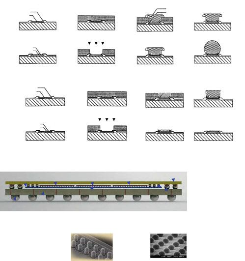
There are many flip-chip bonding/assembly methods, such as: (1) mass reflow of the C4 or C2 bumps with capillary underfill (CUF); (2) thermocompression bonding (TCB) with low force and reflow of C4 or C2 bumps and CUF; (3) TCB with high force and reflow of C2 bumps and nonconductive paste (NCP) ; (4) TCB with high force and reflow of C2 bumps and nonconductive film (NCF); and (5) bumpless low-temperature hybrid bonding, as shown in Fig. 3. Flip-chip bonding/assembly methods (1)–(4) can be applied to chip-to-chip and chip-to-organic, silicon, or ceramic substrates and have been presented in [17, 18]. Herein, only bumpless hybrid bonding, which can only be applied to chip-to-chip and chip-to-silicon substrates, is briefly mentioned (Fig. 1.6).
1.3 Hybrid Bonding
Hybrid bonding was invented by Research Triangle Institute (RTI). They started off with the ZiBond (a direct oxide to oxide bonding that involves wafer-to-wafer processing at low temperatures to initiate high bond strengths). Between 2000 and 2001, Fountain, Enguist, Tong, and several other colleagues founded Ziptronic as a spin-out of RTI. Between 2004 and 2005, based on their ZiBond technology, Ziptronic combined the dielectric bond with embedded metal to simultaneously bond wafers and form the interconnects at lowtemperature, so-called DBI (direct bond interconnect) [19, 20]. Ziptronic was acquired by Tessera on August 28, 2015. Tessera changed its name to Xperi on February 23, 2017. In 2022, Xperi was renamed to Adeia Inc. The breakthrough for Ziptronic DBI technology came in the spring of 2015 when Sony, already using its “Zibond” oxide to oxide bonding technology extended its license to include DBI. DBI is now being used for much of the CMOS (Complementary Metal–Oxide–Semiconductor) image sensor market in the world’s smartphones and other image-based devices. Also, for example, YMTC (Yangtze Memory Technologies Co., Ltd.) is using the Ziptronix DBI technology in its 232-layer 3D NAND with a density of 15.2 GB/mm2 products.
(a) Mass reflow of C4 or C2 Bumps (CUF)
(b) TCB with Low-Force and reflow of C4 or C2 Bumps (CUF)
(c) TCB with High-Force and reflow of C2 Bumps (NCP)
(d) TCB with High-Force and reflow of C2 Bumps (NCF)
Bump less
Bump less
(e) Bumpless Hybrid Bonding
Fig. 1.6 Flip-chip assembly and bonding. a Mass reflows of C4 or C2 bumps (CUF). b TCB with low force and reflow of C4 or C2 bumps (CUF). c TCB with high force and reflow of C2 bumps (NCP). d TCB with high force and reflow of C2 bumps (NCF). e Bumpless hybrid bonding
1.3.1 Some Fundamental on Hybrid Bonding
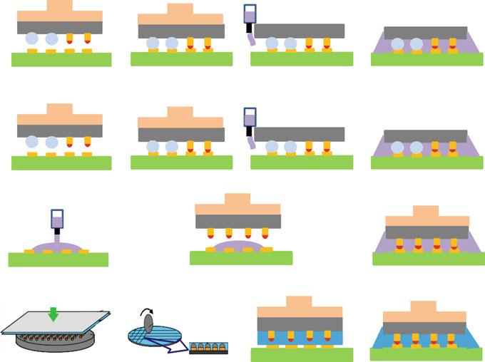
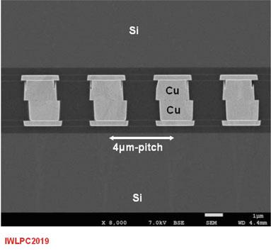
Figure 1.7 shows the key process steps for the bumpless low-temperature DBI [19–43]. First, controlling nanoscale topography is very important for DBI technology. The dielectric surface should be extremely flat and smooth before activation and bonding. Chemical–mechanical polishing (CMP) should achieve a very low dielectric roughness (< 0.5 nm rms) and a certain recess of metal areas below the dielectric surface, as shown in Fig. 1.7a. Upon contact, the dry plasma-activated dielectric surfaces bond together instantaneously, as shown in Fig. 1.7b, at room temperature. (Very high bond energies can be obtained at very low temperatures, as shown in [26]). The dishing gap can be closed by heating, as shown in Fig. 1.7c. (This step is optional because the dishing gap can also be closed by the following subsequent annealing step.) Metal-to-metal bond occurs during batch annealing. The coefficient of thermal
expansion (CTE) of metals is typically far larger than dielectrics. The metal expands to fill the gap and then builds up the internal pressure, as shown in Fig. 1.7d. It is under this internal pressure and annealing temperature that metal atoms diffuse across the interface, making a good metal-to-metal bond and, hence, electrical connection [26]. External pressure is optional for this type of bonding. In this case, the copper oxidation during bonding is minimized because the bonded oxide layer surrounding the copper interconnect protects the interconnect from oxidation in the annealing oven, thus minimizing Cu oxidation during the anneal. The bonded oxide surface also hermetically seals the Cu interconnect during operation. Optimizing the CMP condition is the key to producing the right amount of surface characteristics, such as metal recess, dielectric roughness, and dielectric curvature for DBI [26]. Figure 1.7 shows an optimal DBI with 4 μm-pitch and 2 μm-diameter pads.
(d)
Fig. 1.7 Key process steps (fundamental) of hybrid bonding. a Metal (Cu) recess = 3 nm plasma surface activation. b Oxide-to-oxide initial bond at room temperature. c Heating closes dishing gap (metal CTE > oxide CTE) (optional). d Annealing (e.g., 300 °C for 0.5 h) w/o external pressure
1.3.2 Sony’s CIS with Hybrid Bonding
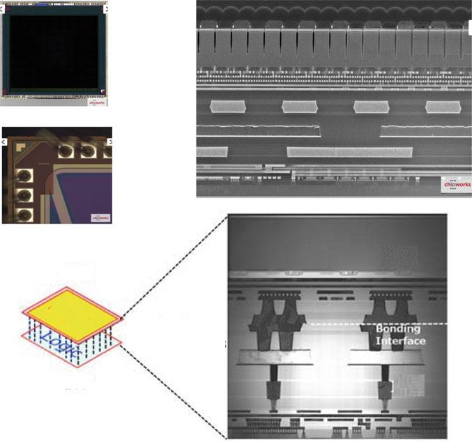
Sony is the first to use bumpless low-temperature Cu–Cu DBI in high-volume manufacturing (HVM) [21, 22]. Sony produced the IMX260 backside-illuminated CMOS image sensor (BI-CIS) for the Samsung Galaxy S7, which shipped in 2016. Electrical test results showed that their robust Cu–Cu direct hybrid bonding achieved remarkable connectivity and reliability. The performance of the image sensor was also super. Top and cross section views of the IMX260 BI-CIS are shown in Fig. 1.8 It can be seen that, unlike in [44] for Sony’s ISX014 stacked camera sensor, the TSVs are eliminated, and the interconnects between the BI-CIS chip and the processor chip are achieved by Cu–Cu DBI. The signals are coming from the package substrate with wire bonds to the edges of the processor chip. Usually, wafer-to-wafer bonding is for the same chip size from both wafers. In Sony’s case, the processor chip is slightly larger than the pixel chip. In order to
Fig. 1.8
Sony’s CMOS image sensor manufactured by hybrid bonding