Introduction
1.1MEMS and Optical MEMS
Micro-Electro-Mechanical Systems (MEMS) is the technology of integrated mechanical and electro-mechanical micro-elements on a single chip. The micro-scale moving components of MEMS devices can be readily and robustly fabricated using the welldeveloped micro/nano fabrication techniques (details are covered in Chap. 3). Mechanical displacement in MEMS devices can be obtained via external electrical actuation. MEMS technology aims to revolutionize nearly every product group by substituting sensors, actuators, detectors, and gears with micrometer-scale equivalents [1–3].
Since its early proposal and demonstration in late 1980s, major advancements have taken place motivated by urgent requirements for large scale production of miniaturized and compact sensors and actuators.
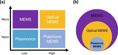
One of the main reasons for the development of MEMS technology in recent years, is the drastic reduction of the size of the device components along with the additional and complemented mechanical modulation functionality which can enable tunable on-chip sensors and actuators [4, 5]. MEMS can provide microstructures in a variety of desirable shapes and sizes with critical future size of micro or nano meter along with significant mechanical tunability as shown in Fig. 1.1.
MEMS devices have been realized using a variety of materials including semiconductors, polymers, glasses, ceramics, metals, and various other alloys. But Silicon, as a horse power in IC industry, and due to a very mature and well-developed fabrication processes, has found a distinctive place in MEMS [3].
The precision mechanics of MEMS technology and micromachining have ignited the possibility of using this technology for a wide variety of applications in high-speed digital
© The Author(s), under exclusive license to Springer Nature Switzerland AG 2023 J. X. J. Zhang, Plasmonic MEMS, Synthesis Lectures on Materials and Optics, https://doi.org/10.1007/978-3-031-23137-7_1
Fig. 1.1 The framework of MEMS, Optical MEMS, Plasmonics, and Plasmonic MEMS. a Comparison by the critical feature size and the optomechanical tunability. b Classified view of each field. Plasmonic MEMS can be considered as a subset of optical MEMS with plasmonic materials and components
circuits [6], radio frequency (RF) and Infrared (IR) devices [7, 8], wireless communications and nanosatellites [9], unmanned air vehicles (UAVs) [10], optical detectors [11], biomedical devices and imaging [12–14], to name a few.
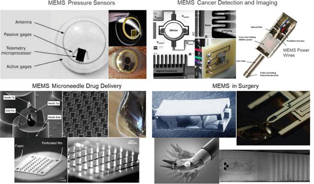
Integration of MEMS with biomedical devices has opened up a new world of possibilities for medical applications. Healthcare industry such as pharmaceuticals, healthcare equipment, biotechnology and related life sciences possess a significant demand for biomedical MEMS (Bio-MEMS). Figure 1.2 shows a few representative BioMEMS apparatuses.
Fig. 1.2 A few BioMEMS representative applications including MEMS pressure sensors, MEMS cancer detection and imaging, MEMS microneedles drug delivery, and MEMS in surgery. Images are taken from top-left [15, 16], top-right [12, 17], bottom left [18, 19], bottom right [20–22]
One of the first MEMS devices to be utilized in the biomedical and bioengineering community were pressure sensors in the late 1980s [23]. In one of the pioneering works, Leonardi, et al. realized the first wireless contact lens for intraocular pressure (IOP) monitoring using a miniaturized MEMS biosensor integrated with biocompatible materials to detect deformations of the eyeball. The device can be used to treat very complex diseases such as Glaucoma. The wireless sensor was built using a microprocessor and an antenna integrated into the soft contact lens shown in Fig. 1.2. The MEMS pressure sensor consists of passive strain gages to determine corneal curvature alterations in response to IOP.
Cancer is among the leading causes of death worldwide. Among different types of cancer, the death rate for oral and oropharyngeal cancer is significantly higher [16]. Wang et al. realized a MEMS enabled handheld high resolution confocal imaging probe for portable oral cancer detection [17]. Record high field of view was achieved using a programmable MEMS micromirror as shown in Fig. 1.2. The MEMS device utilizes a voltage-controlled biaxial gimbal structure to rotate along the two perpendicular axes. The realized handheld scanner imaging device illustrates great promise as a prospective clinical tool for cancer risk assessment, evaluation and treatment.
MEMS can enable microneedles (needles orders of magnitude smaller than the conventional ones) for drug delivery, vaccine delivery and fluid sampling and analysis. These microneedles can be manufactured using a variety of materials including glass, ceramics, silicon, bio-compatible polymers and also water-soluble materials [19, 24]. Scanning electron microscope (SEM) photographs of e few microneedles are presented in Fig. 1.2. Authors in [25] carried out the first human study to show that microneedles are painless. 400 microneedles in an area of 3 × 3 mm used in this study. Each microneedle was approximately 150 µm tall with a base diameter of 80 µm and the tip radius curvature of 1 µm. Many commercialized microneedles have been developed for a variety of applications such as monitoring and controlling blood glucose levels, transdermal micro-projection delivery, and treating alopecia and skin restoration.
Minimally invasive surgery (MIS) is a type of procedure done to limit the size of incision (cut). Advantages of MIS are less scarring, less injury to tissue, shorter hospital stays and less pain. MEMS based microsurgical tools such as microtweezers, microsensors, and microgrippers have been ascertained as a central enabling technology for MIS. A pair of microgrippers and a temperature sensor embedded in robotic microgripper for surgical applications are shown in Fig. 1.2 [22]. One very important and revolutionary aspect of MEMS as a pressure sensor in MIS is to distinguish between different types of tissue during the surgery. This helps the surgeon to identify the proper tissue before making any incision. Menciassi et al. [26] reported a pioneering and an inventive MEMS device for the palpation of tissue using strain gauges. The realized microgripper apparatus was fabricated using an electroplated nickel covered with a thin gold layer, with an overall width of about 7.5 mm and a thickness of 0.4 mm. An overall displacement of 17 µmat the fingertips was achieved using flexure joints.
Photonics; the science of generating and harnessing light, are among the research fields touched by the MEMS technology. The pioneering paper of Petersen’s on silicon scanner [27] galvanized the extensive interest in optical MEMS. Since then, optical MEMS have led to the development of MEMS tunable digital displays [28], deformable mirrors [29], tunable photonic crystal [30], adjustable lenses and apertures [31], endoscopic imaging devices [32], and optical telecommunication systems [33]. The application of optical MEMS scanning has resulted in miniaturized devices for biomedical applications such 3D imaging devices for in vivo diagnostics [34], MEMS based optical biopsy [35], and optical coherence tomography (OCT) systems [13, 32].
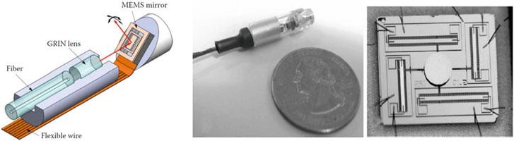
Figure 1.3 shows an optical MEMS enabled endoscopic OCT imaging system. Since its first demonstration by Pan et al. [37], MEMS based endoscopic devices have made significant progress and improvements and currently are being used a vast majority of endoscopic OCT imaging devices. Shown in Fig. 1.3b, is the first 3D endoscopic optical biopsy system. This device is capable of taking high-resolution, noninvasive in vivo clinical images. The integrated optical MEMS scanning micromirror exploits a 2D gimbal-less vertical comb and operates at resonant frequencies of 1.8 and 2.4 kHz in x and y directions respectively. Interested readers can refer to more comprehensive and dedicated textbooks and review papers for more in-depth discussion on fundamentals and recent advances in optical MEMS [3, 33, 38].
. Plasmonics (brief principle, physics and recent development)
Nanophotonics, the study of light at the nanoscale, has become a vibrant field of research, as the flow of light can be manipulated at length scales far below the optical wavelength, largely surpassing the classical limits imposed by diffraction. Driven by remarkable advances in micro/nanofabrication, atomic-resolution imaging, and ultrafast laser technologies, the interface between nanophotonics and MEMS has attested a tremendous progress in the past few years. Prime examples include compact systems for optical communication and interconnects [11, 39, 40], high resolution display [41], ultrafast cameras
1.3 a Schematic of a MEMS-tunable endoscopic OCT probe. b realized MEMS-based OCT probe. c Two-axis MEMS micromirror [36]
(a)
(b)
(c)
Fig.
Fig. 1.4 Diffraction pattern appears as the distance between two optical emitters reduces and the radiation pattern of the two sources are indistinguishable
and photon detectors [42], and novel optical sensors for clinical and security concerns [43].
Conventional photonic devices are limited by diffraction. The diffraction limit is an optical effect which encumbers the progress toward the miniaturization of photonic devices by preventing localization of electromagnetic waves into nanoscale regions; scales much smaller than the wavelength. One important conclusion is that light will diffract when it propagates through a hole or a slit which is smaller than approximately half of its wavelength (Fig. 1.4).
The diffraction pattern follows a simple but intuitive formula. That is
where n is the refractive index, θ is the angle of incidence, and NA is the numerical aperture of the lens.
Plasmonics, the study of the interaction between electromagnetic field and free electrons in a metal, provides a solution to this dilemma. In plasmonic devices, free electrons in the metal can be excited by the electric component of light to have collective oscillations. Using metallic and dielectric nanostructures precisely sculpted into two-dimensional (2D) and 3D nanoarchitectures, light can be scattered, refracted, confined, filtered, and processed in fascinating new ways that are impossible to achieve with natural materials and in conventional geometries. Strictly speaking, plasmonics; investigates plasmons; quanta of collective oscillations of the conduction electrons in a plasma. Plasmonics can squeeze light into dimensions far beyond the diffraction limit by coupling light with the surface collective oscillation of free electrons at the interface of a metal and a dielectric [44]. This control over light at the nanoscale has not only unveiled a plethora of new phenomena but has also led to a variety of relevant applications, including new venues for integrated circuitry, optical computing, solar, and medical technologies, setting high expectations for many novel discoveries in the years to come.
Four classical types of plasmons include, surface plasmon polaritons (SPPs), surface plasmon resonances (SPRs), localized surface plasmons (LSPs), and spoof plasmons.
SPPs result from the interaction of excited electrons with polarized light at the interface between a negative and positive permittivity materials. SPPs are propagating modes with well-defined frequency and wavevector and are evanescently confined in the direction
perpendicular to the propagation. This interaction gives rise to a new type of quasiparticle called polaritons. Polaritons originate from strong light-matter interaction (strong confinement) [45].
SPRs refers to resonances instigating from the collective oscillations of electrons in metals at the interface due to Coulombic interaction with positive background. To excite SPPs, polarized incident photons (light must be polarized to excite the longitudinal mode) and SPRs must have the same frequency and wave vector.
LSPs are generated when electromagnetic field interacts with conduction electrons on the surface of a conductive nanoparticle of size comparable to or smaller than the excitation wavelength. LSPs are non-propagating excitations.
Metals have negative permittivity in the Visible and Ultraviolet regimes of the electromagnetic spectrum, thus support surface plasmons. However, when the wavelength is increased to the Infrared (IR) and Terahertz (THz) regions metals act as perfect electric conductors (PEC). Spoof plasmons are guided leaky waves in the IR and THz regions which can be recognized in metal surfaces patterned with periodic subwavelength grooves, holes and nanowires [46]. A wide selection of materials can support surface plasmons. Please see [47–49] for comprehensive review on plasmonic materials.
Tunable functionality of plasmonic devices is of outmost importance for realizing active and reconfigurable optoelectronic devices. Several modulation techniques can be used to achieve tunable response from plasmonic devices including electrical, optical, and mechanical modulation [50]. Active manipulation of surface plasmons provides a course to tweak the optical functionalities of the plasmonic structure and could be used in light modulators, plasmonic switches and spectrometers to name a few.
1.2Plasmonic MEMS: A Frontier of Photonic Devices
Plasmonic MEMS is a rising field, inspired by the concepts of optical metamaterials and the peculiar features of plasmonic nanopatterns. Low-profile patterned plasmonic surfaces are synergized with a broad class of silicon microstructures, to greatly enhance nearfield nanoscale imaging, sensing and energy harvesting coupled with far-field free-space detection. The concept has demonstrated impact on several key areas from ultra-compact Microsystems for sensitive detection of small number of target molecules, and “surface” as devices for optical data storage to microimaging and displaying.
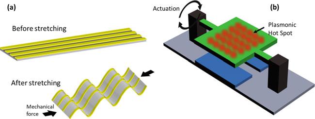
Plasmonic MEMS is evolving into a novel paradigm for the conception of optical plasmonic surfaces. Depending on the intrinsic material properties, different materials response distinctively to the applied voltage. This will allow a wide variety of plasmonic structure to be placed on electromechanically modulated substrate to control their optical spectrum. The idea is schematically shown in Fig. 1.5a. Another option, is to directly pattern a plasmonic grating or structure on the surface of a MEMS device as shown in Fig. 1.5b.
Fig. 1.5 Plasmonic MEMS. a Mechanical modulation of a plasmonics grating via stretchable substrate. b Integration of a plasmonic array with a MEMS device
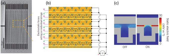
The first experimental demonstration of electromechanically reconfigurable plasmonic structures was reported in 2013 by Ou and colleagues [51], in which they designed a reconfigurable plasmonic metamaterial operating in the near-infrared (NIR). Arrays of 50nm-thick gold meander wires and near parallel gold wires was etched on a 50-nm-thick silicon nitride substrate by focused ion beam (FIB), (details of the fabrication method are explained in Chap. 3). To provide a flexible and robust platform to contain the gold pattern, the silicon nitride substrate is cut into 500 and 250 nm strings for the meander wires and parallel gold wires, respectively. The SEM of the structure with total dimensions of 12 mm × 35 mm is shown in Fig. 1.6a.
The major idea is to exploit the instigating electrostatic forces upon applying electric voltage to mechanically modulate the optical response of the patterned metamaterial. As it can be seen in Fig. 1.6c, applying a small voltage can decrease the gap between the meander wires and parallel wires. This dramatically affects the optical response of the transmitted wave.
Fig. 1.6 First demonstration of an electrostatically actuated tunable plasmonic metamaterial. (a )SEM image(b) electrostatic forces acting on individual strings (c ) static electric field simulations
The first thermomechanicaly tunable plasmonic MEMS device was reported in 2011 by the pioneering work of Ou et al. [52]. The device consists of gold plasmonic splitring resonators (SRRs) supported by interchanging thermally tunable silicon nitride/gold bridges (silicon nitride and gold both have large thermal expansion coefficient). Their realized photonic metamaterial device operates three orders of magnitude faster than formerly reached modulation rate for the NIR spectrum. Potential applications of the device include tunable sensors, modulators, and spectral filters.
The first light-controlled plasmonic MEMS device was attained in the NIR regime via patterning asymmetrically spaced gold elements on silicon nitride strips [53]. The authors demonstrated that through pump-probe experiment with ultrafast laser diodes operating at 1550 and 1310 nm, large modulation of transmission can be achieved with milliwatt power levels. The photo-addressable capacitance can be cooled down in highspeed timescales on the order of 20 µs. Light modulated plasmonic devices can be used to realize reconfigurable nonlinear metadevices.
In summary, the paradigm of plasmonic MEMS enables low-profile conformal surfaces on microdevices, rather than a bulk material or coatings, which may provide clear advantages for the physical, chemical and biological-related sensing, imaging, light harvesting applications in addition to significantly easier realization, enhanced flexibility and tunability.
1.3Status of the Field
In last few years, Plasmonic MEMS has developed tremendously. A summary of some landmark papers in the field are presented in Table 1.1. A more comprehensive table can be found in Appendix 1.
Despite recent advances in the field and the growing number of published works, many more ideas need to be explored. We believe that the tremendous obtainable opportunities in combining plasmonics with MEMS still remains largely underexploited and underexplored. Almost all current plasmonic MEMS devices and architectures exploit conventional metal plasmonics. We predict the field to branch out towards combining highly doped semiconductors as a plasmonic material for the Infrared and THz region. This indeed can instigate fields beyond plasmonics MEMS and give birth to fields such as epsilon-near zero (ENZ) MEMS.
Beside using metallic or highly doped semiconductor resonator, dielectric Mie resonators can also be integrated with MEMS technology to realized highly localized fields and tunable dielectric metamaterials and metasurfaces.
Year
2010 [ 54 ]
2011 [ 52 ]
2013 [ 51 ]
2015 [ 53 ]
Application
Fabrication method
Flexible, stretchable, nonplanar electronic and photonic systems
Electron beam lithography
Reversible and large-range tunable metamaterials
Focused ion beam
Tunable spectral filters, switches, and modulators
Focused ion beam
Modulating light with light
Focused ion beam
Material
Landmark papers in the field of plasmonic MEMS
Table 1.1
Importance
Control mechanism
PDMS substrate, gold nanorod
First demonstration of a flexible plasmonic device
Silicon nitride membrane, gold
First demonstration of a thermomechanical plasmonic device
Mechanical force
Device
Flexible plasmonics
Thermomechanical
Reconfigurable metamaterials
Silicon nitride substrate, gold wires
First demonstration of an electrostatic plasmonic device
Electromechanical
Reconfigurable metamaterials
Gold on silicon nitride strips
First demonstration of an optomechanical plasmonic device
Optomechanical
Tunable modulator
1.4Existing Challenges
Emerging concepts, designs and applications of plasmonic MEMS have been demonstrated in the recent years, ranging from plasmonic gas and chemical sensors, microfilters for circulating tumor cells (CTC) capturing, DNA biosensing among many others. Fascinating new concepts explored in detail in the framework of this review, with the goal to devise new geometries on MEMS surfaces that may for example require no moving structures to tilt the radiated beam in the desired direction. We expect that the combination of design theory, modeling and experimental implementation may provide full degrees of freedom and enhanced performance for future plasmonic MEMS designs for specific applications.
Although many promising results have been reported, several challenges remain untouched. These challenges can be considered in three aspects.
1. Materials innovation are much needed to provide seamlessly integrated mechanical, optical, materials properties suitable for plasmonic MEMS; Emerging computational materials design approaches may be used to guide the development of new materials with unique properties for plasmonic operation under various physical and chemical conditions. In addition, just as the electronic devices, the performance of optical devices can be influenced by material stress and strain degradation. New materials to prevent large degradation of MEMS devices need to be realized. Also, Plasmonic MEMS for bioelectronic and bioengineering applications appear to be one of the most persuasive areas. The interface between devices and biology needs to be well considered, for example, for needed biocompatibility while maintaining core device functionalities.
2. New design strategies, through theoretical modeling and numerical simulations, enable fast, high throughput and flexible operations; high energy consumption of MEMS devices compared to the electronic counterparts hinder their path for large scale integration. Reducing the energy consumption of plasmonic MEMS devices demands urgent attention. While, megahertz modulation rates have been demonstrated and reported in the literature, faster modulation in the order of gigahertz is required. New design strategies might be able to push the field towards higher modulation rates.
3. Micro-nanofabrication advancement combined with smart geometric mechanics for compact implementation; patterning flexible plasmonic substrates with new design paradigms such as Origami and Kirigami needs to be explored. This can also open up new directions to realize high-contrast switching of plasmonic MEMS devices.
In this book, we discuss the theory, fabrication, and application of plasmonic MEMS and the recent progresses in the field for biosensing applications. We believe that the optical plasmonic surface on MEMS concept may constitute the much sought flexible and reliable bridge between near-field sensing, imaging at the nanoscale and far-field detection. In our
vision, these concepts may be combined to realize a fascinating paradigm to manipulate light at will with a clear impact on several key areas of interest for MEMS in the broad area of sensing, imaging, light harvesting applications in addition to significantly easier realization, enhanced flexibility and tunability.
References
1. M. Tanaka, “An industrial and applied review of new MEMS devices features,” Microelectronic Engineering, vol. 84, pp. 1341–1344, 2007/05/01/ 2007.
2. S. Yang and Q. Xu, “A review on actuation and sensing techniques for MEMS-based microgrippers,” Journal of Micro-Bio Robotics, vol. 13, pp. 1-14, October 01 2017.
3. O. Solgaard, Photonic microsystems: Micro and nanotechnology applied to optical devices and systems: Springer Science & Business Media, 2009.
4. H. T. Chorsi, M. T. Chorsi, and S. D. Gedney, “A Conceptual Study of Microelectromechanical Disk Resonators,” IEEE Journal on Multiscale and Multiphysics Computational Techniques, vol. 2, pp. 29-37, 2017.
5. M. T. Chorsi and H. T. Chorsi, “Modeling and analysis of MEMS disk resonators,” Microsystem Technologies, vol. 24, pp. 2517-2528, June 01 2018.
6. S. Tabatabaei and A. Partridge, “Silicon MEMS Oscillators for High-Speed Digital Systems,” IEEE Micro, vol. 30, pp. 80-89, 2010.
7. C. A. Musca, J. Antoszewski, K. J. Winchester, A. J. Keating, T. Nguyen, K. K. M. B. D. Silva, et al., “Monolithic integration of an infrared photon detector with a MEMS-based tunable filter,” IEEE Electron Device Letters, vol. 26, pp. 888-890, 2005.
8. J. Sha, W. Chen, K. Yan, J. Luo, R. Xu, D. Yao,etal., “Tunable Metamaterial IR Emitter by Using MEMS Microheater,” in 2018 International Conference on Optical MEMS and Nanophotonics (OMN), 2018, pp. 1–2.
9. M. Mihailovic, T. V. Mathew, J. F. Creemer, B. T. C. Zandbergen, and P. M. Sarro, “MEMS silicon-based resistojet micro-thruster for attitude control of nano-satellites,” in 2011 16th International Solid-State Sensors, Actuators and Microsystems Conference, 2011, pp. 262–265.
10. J. Wendel, O. Meister, C. Schlaile, and G. F. Trommer, “An integrated GPS/MEMS-IMU navigation system for an autonomous helicopter,” Aerospace Science and Technology, vol. 10, pp. 527–533, 2006/09/01/ 2006.
11. M. C. Wu, O. Solgaard, and J. E. Ford, “Optical MEMS for Lightwave Communication,” Journal of Lightwave Technology, vol. 24, pp. 4433-4454, 2006.
12. Y. Wang, S. Bish, J. W. Tunnell, and X. J. Zhang, “MEMS scanner enabled real-time depth sensitive hyperspectral imaging of biological tissue,” Optics Express, vol. 18, pp. 24101–24108, 2010/11/08 2010.
13. K. Karthik, C. C. Jonathan, M. Austin, J. K. Nate, H. Kazunori, E. M. Thomas,etal.,“Fast 3D in vivo swept-source optical coherence tomography using a two-axis MEMS scanning micromirror,” Journal of Optics A: Pure and Applied Optics, vol. 10, p. 044013, 2008.
14. Y. Wang, S. Bish, J. W. Tunnell, and X. J. Zhang, “MEMS scanner based handheld fluorescence hyperspectral imaging system,” Sensors and Actuators A: Physical, vol. 188, pp. 450–455, 2012/12/01/ 2012.
15. M. Leonardi, E. M. Pitchon, A. Bertsch, P. Renaud, and A. Mermoud, “Wireless contact lens sensor for intraocular pressure monitoring: assessment on enucleated pig eyes,” Acta Ophthalmologica, vol. 87, pp. 433-437, 2009.
16. Available: https://www.sensimed.ch/
17. W. Youmin, R. Milan, H. S. McGuff, B. Gauri, Y. Bin, S. Ting,etal., “Portable oral cancer detection using a miniature confocal imaging probe with a large field of view,” Journal of Micromechanics and Microengineering, vol. 22, p. 065001, 2012.
18. P. Zhang, C. Dalton, and G. A. Jullien, “Design and fabrication of MEMS-based microneedle arrays for medical applications,” Microsystem Technologies, vol. 15, pp. 1073-1082, July 01 2009.
19. E. Larrañeta, R. E. M. Lutton, A. D. Woolfson, and R. F. Donnelly, “Microneedle arrays as transdermal and intradermal drug delivery systems: Materials science, manufacture and commercial development,” Materials Science and Engineering: R: Reports, vol. 104, pp. 1–32, 2016/06/01/ 2016.
20. A. P. Lee, D. R. Ciarlo, P. A. Krulevitch, S. Lehew, J. Trevino, and M. A. Northrup, “A practical microgripper by fine alignment, eutectic bonding and SMA actuation,” Sensors and Actuators A: Physical, vol. 54, pp. 755–759, 1996/06/01/ 1996.
21. M. Kumemura, D. Collard, S. Yoshizawa, D. Fourmy, N. Lafitte, L. Jalabert,etal., “Direct biomechanical sensing of enzymatic reaction On DNA by silicon nanotweezers,” in 2010 IEEE 23rd International Conference on Micro Electro Mechanical Systems (MEMS), 2010, pp. 915–918.
22. R. K. J, “Applications of MEMS in surgery,” Proceedings of the IEEE, vol. 92, pp. 43–55, 2004.
23. W. P. Eaton and J. H. Smith, “Micromachined pressure sensors: review and recent developments,” Smart Materials and Structures, vol. 6, p. 530, 1997.
24. R. F. Donnelly, T. R. R. Singh, and A. D. Woolfson, “Microneedle-based drug delivery systems: Microfabrication, drug delivery, and safety,” Drug Delivery, vol. 17, pp. 187–207, 2010/05/01 2010.
25. S. Kaushik, A. H. Hord, D. D. Denson, D. V. McAllister, S. Smitra, M. G. Allen,etal.,“Lack of Pain Associated with Microfabricated Microneedles,” Anesthesia & Analgesia, vol. 92, pp. 502504, 2001.
26. A. Menciassi, A. Eisinberg, G. Scalari, C. Anticoli, M. C. Carrozza, and P. Dario, “Force feedback-based microinstrument for measuring tissue properties and pulse in microsurgery,” in Proceedings 2001 ICRA. IEEE International Conference on Robotics and Automation (Cat. No.01CH37164), 2001, pp. 626–631 vol. 1.
27. K. E. Petersen, “Silicon Torsional Scanning Mirror,” IBM Journal of Research and Development, vol. 24, pp. 631-637, 1980.
28. C. Liao and J. Tsai, “The Evolution of MEMS Displays,” IEEE Transactions on Industrial Electronics, vol. 56, pp. 1057-1065, 2009.
29. T. Bifano, “MEMS deformable mirrors,” Nature Photonics, vol. 5, p. 21, 01/01/online 2011.
30. Y. H. Cui, Q. Wu, W. Park, J. Jeon, M. J. Kim, and J. Lee, “Mems-based mechanically tunable flexible photonic crystal,” in TRANSDUCERS 2009-2009 International Solid-State Sensors, Actuators and Microsystems Conference, 2009, pp. 509–512.
31. Y. Zou, W. Zhang, F. S. Chau, and G. Zhou, Miniature adjustable-focus endoscope using a MEMS Alvarez lens, in 2015 International Conference on Optical MEMS and Nanophotonics (OMN), 2015, pp. 1–2.
32. J. Sun and H. Xie, “MEMS-Based Endoscopic Optical Coherence Tomography,” International Journal of Optics, vol. 2011, 2011.
33. O. Solgaard, A. A. Godil, R. T. Howe, L. P. Lee, Y. Peter, and H. Zappe, “Optical MEMS: From Micromirrors to Complex Systems,” Journal of Microelectromechanical Systems, vol. 23, pp. 517-538, 2014.
34. W. Piyawattanametha, E. D. Cocker, L. D. Burns, R. P. J. Barretto, J. C. Jung, H. Ra,etal., “In vivo brain imaging using a portable 2.9 g two-photon microscope based on a microelectromechanical systems scanning mirror,” Optics Letters, vol. 34, pp. 2309–2311, 2009/08/01 2009.
35. D. T. McCormick, W. Jung, Y. Ahn, Z. Chen, and N. C. Tien, “A Three Dimensional Real-Time MEMS Based Optical Biopsy System for In-Vivo Clinical Imaging,” in TRANSDUCERS 20072007 International Solid-State Sensors, Actuators and Microsystems Conference, 2007, pp. 203–208.
36. W. Jung, D. T. McCormick, Y.-C. Ahn, A. Sepehr, M. Brenner, B. Wong,etal.,“In vivo three-dimensional spectral domain endoscopic optical coherence tomography using a microelectromechanical system mirror,” Optics Letters, vol. 32, pp. 3239–3241, 2007/11/15 2007.
37. Y. Pan, H. Xie, and G. K. Fedder, “Endoscopic optical coherence tomography based on a microelectromechanical mirror,” Optics Letters, vol. 26, pp. 1966–1968, 2001/12/15 2001.
38. G. Zhou and C. Lee, Optical MEMS, Nanophotonics, and Their Applications: CRC Press, 2017.
39. J. E. Ford, V. A. Aksyuk, D. J. Bishop, and J. A. Walker, “Wavelength Add-Drop Switching Using Tilting Micromirrors,” Journal of Lightwave Technology, vol. 17, p. 904, 1999/05/01 1999.
40. D. J. Bishop, C. R. Giles, and G. P. Austin, “The Lucent LambdaRouter: MEMS technology of the future here today,” IEEE Communications Magazine, vol. 40, pp. 75-79, 2002.
41. J. Ma, “Advanced MEMS-based technologies and displays,” Displays, vol. 37, pp. 2–10, 2015/04/01/ 2015.
42. F. Niklaus, C. Vieider, and H. Jakobsen, “MEMS-based uncooled infrared bolometer arrays: a review,” in Photonics Asia 2007 , 2008, p. 15.
43. X. J. Zhang, S. Zappe, R. W. Bernstein, O. Sahin, C. C. Chen, M. Fish,etal., “Micromachined silicon force sensor based on diffractive optical encoders for characterization of microinjection,” Sensors and Actuators A: Physical, vol. 114, pp. 197–203, 2004/09/01/ 2004.
44. J. A. Schuller, E. S. Barnard, W. Cai, Y. C. Jun, J. S. White, and M. L. Brongersma, “Plasmonics for extreme light concentration and manipulation, Nat Mater,” vol. 9, pp. 193–204, 03//print 2010.
45. D. N. Basov, M. M. Fogler, and F. J. García de Abajo, “Polaritons in van der Waals materials,” Science, vol. 354, 2016.
46. R. Stanley, “Plasmonics in the mid-infrared,” Nature Photonics, vol. 6, p. 409, 06/28/online 2012.
47. A. Boltasseva and H. A. Atwater, “Low-Loss Plasmonic Metamaterials,” Science, vol. 331, pp. 290-291, 2011.
48. P. R. West, S. Ishii, G. V. Naik, N. K. Emani, V. M. Shalaev, and A. Boltasseva, “Searching for better plasmonic materials,” Laser & Photonics Reviews, vol. 4, pp. 795-808, 2010.
49. G. V. Naik, V. M. Shalaev, and A. Boltasseva, “Alternative Plasmonic Materials: Beyond Gold and Silver,” Advanced Materials, vol. 25, pp. 3264-3294, 2013.
50. N. I. Zheludev and E. Plum, “Reconfigurable nanomechanical photonic metamaterials,” Nature Nanotechnology, vol. 11, p. 16, 01/07/online 2016.
51. J.-Y. Ou, E. Plum, J. Zhang, and N. I. Zheludev, “An electromechanically reconfigurable plasmonic metamaterial operating in the near-infrared,” Nature Nanotechnology, vol. 8, p. 252, 03/17/online 2013.
52. J. Y. Ou, E. Plum, L. Jiang, and N. I. Zheludev, “Reconfigurable Photonic Metamaterials,” Nano Letters, vol. 11, pp. 2142–2144, 2011/05/11 2011.
53. J.-Y. Ou, E. Plum, J. Zhang, and N. I. Zheludev, “Modulating light with light via giant nanoopto-mechanical nonlinearity of plasmonic metamaterial,” arXiv preprint arXiv:1506.05852, 2015.
54. I. M. Pryce, K. Aydin, Y. A. Kelaita, R. M. Briggs, and H. A. Atwater, “Highly Strained Compliant Optical Metamaterials with Large Frequency Tunability,” Nano Letters, vol. 10, pp. 4222–4227, 2010/10/13 2010.
Theoretical Foundations
This chapter provides the fundamentals of electromagnetic theory for the book in relation to plasmonic MEMS. First, a brief review of Maxwell’s equations is provided. This is followed by a discussion of general surface waves, dielectric constant of metals, and plasmon dispersion. The next sections of the chapter focus on the intersection of memes and plasmonics and reviews the theories relevant to plasmonics MEMS in the literature.
2.1Maxwell’s Equations and Electromagnetic Wave Theory
Considering the classical and semi-classical wave nature of light, Maxwell’s equations in a conventional macroscopic framework can be used to fully describe the electromagnetic wave interaction with metals. In differential form, Maxwell’s equations can be written as
These equations couple the four macroscopic fields D (the electric flux density), E (the electric field), H (the magnetic field), and B (the magnetic flux density) with the charge density (ρ) and current densities (J = Jc (conduction current density) + Ji (induction current density) + Jd (displacement current density)). In macroscopic frame, current density
© The Author(s), under exclusive license to Springer Nature Switzerland AG 2023 J. X. J. Zhang, Plasmonic MEMS, Synthesis Lectures on Materials and Optics, https://doi.org/10.1007/978-3-031-23137-7_2
is expressed as the product of charge density and velocity for any location in space
In time domain, fields can be related via the constitutive relations
where ε 0 [Farads/meter] and μ0 [Henries/meter] are the permittivity and the permeability of the vacuum, respectively. For an isotropic, linear, and nonmagnetic approximation, the constitutive relations can be written as:
where ε r and μr are the relative permittivity and relative permeability, respectively. the electric polarization P and magnetization M consider the properties of the medium. The conduction current density Jc is related to the electric field using
where σ [siemens/meter] is the conductivity of the medium.
To derive the wave equation, we take the curl of Eq. (2.1). Using Eq. (2.2), for a source-free region, the wave equation can be written as
Here ε and μ are the electric permittivity (also called absolute permittivity, ε = ε0 εr )and magnetic permeability (μ = μ0 μr ). Equation (2.11) is actually three equations, which together comprise the x-, y-and z-vector components for the E field vector. The Laplacian in Cartesian coordinates is defined as
The monochromatic solution (a set of complex-traveling wave solutions) to this wave equation has the following form
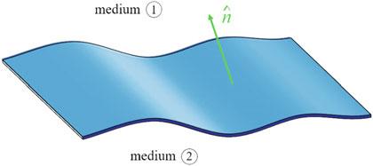
Fig. 2.1 Boundary surface of two media with tangential and normal components
where α quantifies attenuation, β is the propagation constant, ω = kc with c = 1/√ε0 μ0 being the speed of light, and ω k = v phase is the phase velocity. The relation between the phase velocity and the frequency is known as the dispersion relation.
Boundary conditions state how the electromagnetic fields (E, D, H, B) change at the interface between two different materials (Fig. 2.1).
where Jim and ρs are the impressed electric current and surface charge density, respectively. The first two of these state that the tangential electric fields are continuous across the interface, though the tangential magnetic fields are discontinuous at the same location by an amount equal to the impressed electric current. Zenneck [1], more than a century ago, solved the Maxwell’s equations for the planar interface of two different materials and initiated the concept of surface waves. A surface wave is an electromagnetic wave with parallel Poynting vector that propagates along a surface or an interface of two dissimilar media. The propagation of a surface wave is guided by the planar interface and decays exponentially in both media. Surface waves play a key role in studying properties of condensed matter at the interface. A more inclusive and mathematically rigorous derivation of surface waves was later done by Sommerfeld [2], and those surface waves have since become known as the Zenneck waves.
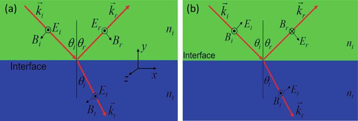
Equations (2.15) through (2.18) can be used to compute the fraction of a light wave reflected and transmitted by a flat interface between two media with different refractive indices (Fig. 2.2).
Applying the boundary conditions to a simple plane wave incident on a single planar interface leads to the Fresnel reflection and transmission coefficients. For TE case, tangential electric field is continuous at the boundary,
The tangential magnetic field is continuous
Using the constitutive relations and considering only the amplitude of the waves ( E 0 ) at the boundary, the following relations can be derived for the reflection and transmission coefficient of TE and TM polarized waves
Fig. 2.2 Fresnel reflection and transmission coefficients. a TE, perpendicular, s-polarized. b TM, parallel, p-polarized, (“s” polarization (aka TE or horizontal) has an E field that is perpendicular to the plane of incidence, “p” polarization (aka TM or vertical) has an E field that is parallel to the plane of incidence), s and p stand for the German words senkrecht (perpendicular) and parallel (parallel)
where n i and n t are the refractive indices of the incident and reflected medium. A plot of Fresnel reflection and transmission coefficients for n = 1.5 is shown in Fig. 2.3.
At some angle, known as the critical angle, light traveling from a higher refractive index medium to a lower refractive index medium will be refracted at 90º. When the angle of incidence exceeds the critical angle, there is no refracted light. All the incident light is reflected back into the medium. The critical angle of incidence can be obtained for two media
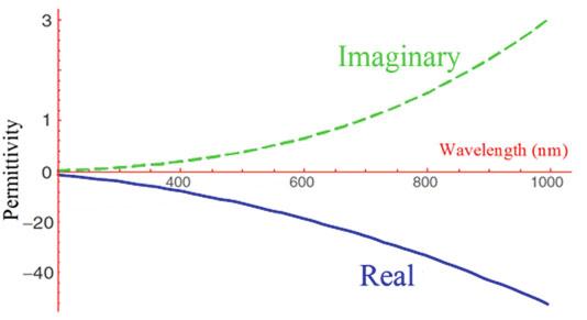
Dielectric constant (relative permittivity) is a measure of the polarizability of a material and can be derived using the Lorentz model and the Drude model for dielectric and metallic materials, respectively. By solving the standard equation of motion for a harmonically bound classical electron, in analogy to the motion of a mass on a spring, we obtain the displacement r (t ) = r 0
where e and me are the charge and effective mass of the free electrons, and E 0 and ω are the amplitude and frequency of the applied electric field (actuation force). The damping term γd is proportional to γd = v F /l ,where v F is the Fermi velocity and l is the electron mean free path between scattering events.
Applying Fourier transform, F (r (t )), we obtain r (ω).Using r (ω) and polarization vector, Lorentz equation can be derived as
Fig. 2.3 Reflections of TE and TM modes for n = 1.5. Brewster’s angle (rTM = 0) is also plotted
here ω p is the plasma frequency, ω0 is the frequency of the restoring force, and ε∞ describes the ionic background. Assuming the free electron model for metal (ω0 = 0), Drude model can be obtained using
If ω is larger than ω p , corresponding refractive index is a real quantity, on the other hand if ω is smaller than ω p , refractive index is imaginary since εm is negative.
The real and imaginary parts of the susceptibility are connected by the KramersKroenig relations (KKR).
Here ℘ means the principal value of the integral.
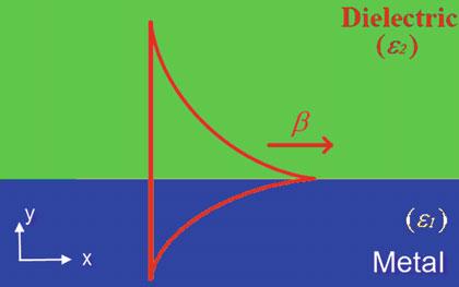
Surface plasmons are surface waves that are the solution of Maxwell’s equations. The simplest geometry supporting SPPs is a single, planar interface between a metal, with a negative dielectric constant εm , (metals at THz region have negative real permittivity as shown in Fig. 2.4) and a dielectric, with a positive dielectric constant as illustrated in Fig. 2.5. This is a critical criterion since in this situation wave can effectively penetrate inside the metal.
Fig. 2.4 Real and imaginary parts of the dielectric constant for gold in visible range of the wavelength according to the Drude model
Fig. 2.5 Schematic view of surface wave propagating along a single metal–dielectric interface
Considering TM excitation (Hz ,Ex , and Ey ) and propagation along the x-direction, i.e. ∂/∂ x = i β ,
Equation (2.31) through (2.33) can be expanded separately for each region in Fig. 2.5
For the dielectric region, i.e. y > 0,
and for the metallic region, i.e. y > 0,