

https://ebookmass.com/product/interface-engineering-inorganic-field-effect-transistors-xuefeng-guo/

Instant digital products (PDF, ePub, MOBI) ready for you
Download now and discover formats that fit your needs...
Effect of electrode Pt-loading and cathode flow-field plate type on the degradation of PEMFC Qu
https://ebookmass.com/product/effect-of-electrode-pt-loading-andcathode-flow-field-plate-type-on-the-degradation-of-pemfc-qu/
ebookmass.com
Brain-Computer Interface M.G. Sumithra
https://ebookmass.com/product/brain-computer-interface-m-g-sumithra/
ebookmass.com
GaN transistors for efficient power conversion Third Edition De Rooij
https://ebookmass.com/product/gan-transistors-for-efficient-powerconversion-third-edition-de-rooij/
ebookmass.com
Heating, Cooling, Lighting: Sustainable Design Methods for Architects 4th
https://ebookmass.com/product/heating-cooling-lighting-sustainabledesign-methods-for-architects-4th/
ebookmass.com


Working with Dual Diagnosis: A Psychosocial Perspective
First Edition Darren Hill
https://ebookmass.com/product/working-with-dual-diagnosis-apsychosocial-perspective-first-edition-darren-hill/
ebookmass.com
The Age of Post-Rationality: Limits of economic reasoning in the 21st century 1st Edition Val Colic-Peisker
https://ebookmass.com/product/the-age-of-post-rationality-limits-ofeconomic-reasoning-in-the-21st-century-1st-edition-val-colic-peisker/
ebookmass.com
Must Know Math Grade 6 1st Edition Nicholas Falletta


https://ebookmass.com/product/must-know-math-grade-6-1st-editionnicholas-falletta/
ebookmass.com
NKJV, Spirit-Filled Life Bible, Third Edition , Genuine Leather, Black, Thumb
https://ebookmass.com/product/nkjv-spirit-filled-life-bible-thirdedition-genuine-leather-black-thumb/
ebookmass.com
The Second World War - Churchill, 2022 John Greehan (Ed)


https://ebookmass.com/product/the-second-world-warchurchill-2022-john-greehan-ed/
ebookmass.com

Xianming Yang (Editor)
https://ebookmass.com/product/chinas-qualitative-economictransformation-1st-edition-xianming-yang-editor/
ebookmass.com

InterfaceEngineeringinOrganicField-EffectTransistors
InterfaceEngineeringinOrganicField-Effect Transistors
XuefengGuo
HongliangChen
Authors
Prof.XuefengGuo PekingUniversity 202ChengfuRd HaidianDistrict 100871Beijing China
Prof.HongliangChen ZhejiangUniversity No.866YuHangTangRd XihuDistrict 310027Hangzhou China
CoverImage: ©blackdovfx/GettyImages
Allbookspublishedby WILEY-VCH arecarefully produced.Nevertheless,authors,editors,and publisherdonotwarranttheinformation containedinthesebooks,includingthisbook, tobefreeoferrors.Readersareadvisedtokeep inmindthatstatements,data,illustrations, proceduraldetailsorotheritemsmay inadvertentlybeinaccurate.
LibraryofCongressCardNo.: appliedfor BritishLibraryCataloguing-in-PublicationData Acataloguerecordforthisbookisavailable fromtheBritishLibrary.
Bibliographicinformationpublishedby theDeutscheNationalbibliothek TheDeutscheNationalbibliotheklists thispublicationintheDeutsche Nationalbibliografie;detailedbibliographic dataareavailableontheInternetat <http://dnb.d-nb.de>
©2023WILEY-VCHGmbH,Boschstraße12, 69469Weinheim,Germany
Allrightsreserved(includingthoseof translationintootherlanguages).Nopartof thisbookmaybereproducedinanyform–by photoprinting,microfilm,oranyother means–nortransmittedortranslatedintoa machinelanguagewithoutwrittenpermission fromthepublishers.Registerednames, trademarks,etc.usedinthisbook,evenwhen notspecificallymarkedassuch,arenottobe consideredunprotectedbylaw.
PrintISBN: 978-3-527-35145-9
ePDFISBN: 978-3-527-84046-5
ePubISBN: 978-3-527-84047-2
oBookISBN: 978-3-527-84048-9
Typesetting Straive,Chennai,India
Contents
Preface ix
AuthorBiographies xi
ListofAcronymsandAbbreviations xiii
1Introduction 1
1.1DifferentInterfacesinOFETs 1
1.2BriefHistoricOverviewofInterfaceEngineeringinOFETs 3
1.3ScopeoftheBook 3
2InterfacialModificationMethods 7
2.1NoncovalentModificationMethods 7
2.1.1ChargeInsertionLayerattheElectrodeSurface 7
2.1.2DielectricSurfacePassivationMethods 9
2.2CovalentModificationMethods 12
2.2.1SAMModificationofElectrodes 12
2.2.2SAMModificationofDielectrics 12
2.2.2.1SAM/SiO2 Dielectrics 14
2.2.2.2SAM/High-k Dielectrics 14
2.2.2.3Self-AssembledMonolayerField-EffectTransistors(SAMFETs) 28
2.3EffortsinDevelopingNewMethods 31
3Semiconductor/SemiconductorInterface 33
3.1InfluenceofAdditivesonaMaterial’sNucleationandMorphology 37
3.1.1SolventAdditives 37
3.1.2NucleatingAgents 41
3.1.3Template-MediatedCrystallization 43
3.1.4BlendingwithInsulatingPolymers 45
3.1.5BlendingwithPolymerElastomer:NanoconfinementEffect 50
3.2EnhancingthePerformanceThroughSemiconductor Heterojunctions 55
3.2.1PlanarBilayerHeterostructures 57
3.2.2Molecular-LevelHeterojunction 61
3.2.3SupramolecularArrangementoftheHeterojunctions 64
3.3IntegratingMolecularFunctionalitiesintoElectricalCircuits 69
3.3.1Charge-Trapping-InducedMemoryEffect 69
3.3.2Photochromism-InducedSwitchingEffect 72
4Semiconductor/ElectrodeInterface 77
4.1WorkFunctionTuningforBetterContact 79
4.1.1SAMModification 80
4.1.2ChargeInsertionLayerModification 84
4.1.3Polymer-BasedElectrodes 89
4.1.4CarbonNanomaterial-BasedElectrodes 92
4.1.5CovalentBondFormationattheMolecularLevel 97
4.2InstallingSwitchingEffectsatSemiconductor/ElectrodeInterface 100
5Semiconductor/DielectricInterface 103
5.1DielectricModificationtoTuneSemiconductorMorphology 105
5.1.1DielectricSurfaceEnergyControl 106
5.1.1.1ModifywithSAM 106
5.1.1.2SurfaceModificationwithPolymers 112
5.1.2DielectricMicrostructureDesign 113
5.1.2.1RoughnessEffect 114
5.1.2.2Nano-fabricationCreatedMicrostructure 116
5.1.2.3Self-assembledMorphologyofDielectric 118
5.2EliminatingInterfacialTraps 120
5.2.1DielectricSurfacePassivation(Treatment)Methods 121
5.2.1.1PolymerEncapsulationofDielectrics 122
5.2.1.2GapDielectrics 124
5.2.2SAM/SiO2 Dielectrics 126
5.2.2.1ProvideEfficientInsulatingBarrierHeight 127
5.2.2.2ControlSurfacePolarityandCarrierDensity 128
5.2.3SAM/High-k Dielectrics 131
5.2.3.1FundamentalsofSAM-ModifiedHigh-k Dielectrics 132
5.2.3.2SAM/High-k HybridDielectricsforFlexibleSubstrate 134
5.2.4Self-assembledMonolayerField-EffectTransistors(SAMFETs) 137
5.2.4.1MoleculeDesignforSAMFETs 137
5.2.4.2MorphologyControlofSAMFET 139
5.3IntegratingNewFunctionalities 141
5.3.1PhotoresponsiveDielectrics 142
5.3.2OtherExternalStimuli-ResponsiveDielectrics 144
5.3.2.1PressureSensor 145
5.3.2.2ThermalSensor 147
5.3.2.3MagneticSensor 147
5.3.2.4MultifunctionalSensor 148
5.3.3IntegratingMemoryEffectattheDielectrics 148
6Semiconductor/EnvironmentInterface 155
6.1DeviceOptimizationtoImproveSensingPerformance 156
6.1.1MonolayerFunctionalization 156
6.1.2BilayerHeterojunctionApproach 158
6.1.3RemoteFloatingGate 159
6.2OECT-BasedandEGOFET-BasedSensors 160
7InterfacingOrganicElectronicswithBiology 165
7.1IntegrationofOFETs/OECTswithNonelectrogenicCells 166
7.2IntegrationofFlexibleBioelectronicswithElectrogenicCells 170
7.3Light/Cell/DeviceInterfaces 174
8ConcludingRemarksandOutlook 179
8.1NewChallengesinMolecularDesign 179
8.2High-QualityOSCFilms:Self-AssemblyControl 180
8.3High-PerformanceScalableFlexibleOptoelectronics 180
8.4ExplorationofNovelStructures:Organic/2DHeterostructuresand VerticalStructures 181
8.5Instability:StabilityinAqueousMediaandThermalStabilityinHygienic Applications 181
8.6MultifunctionalSensorSystems 183
References 185 Index 251
Preface
Thedevelopmentofmicroelectronicsintomodernintegratedcircuitsoverthe past75yearswastheresultofcontinuouseffortsofhugeteamsofscientistsand engineers.Thedeviceperformanceofmicroelectronicdevicesismainlydetermined bythepropertiesofthematerialsusedandtheircorrespondinginterfaces,justas NobellaureateHerbertKroemercoined,“theinterfaceisthedevice.”Understandingandgoverningthechargetransferphenomenaoccurringattheinterfacescould revolutionizeanumberofrelatedfields,includingbatteries,catalysis,datastorage, energyharvesting,imagingdisplays,sensingdevices,andevensolarcells.Forthese reasons,interfaceengineeringoftheseheterojunctionshascapturedtheattention ofabroadcrosssectionofscientificandindustrialcommunities.
Incomparisonwithtraditionalcomplementarymetaloxidesemiconductor transistors,theadvantagesoforganicfield-effecttransistors(OFETs)originatefrom howOFETscanbemanufactured,includingtheconsiderablevarietyinmolecular design,lowcost,lightweight,mechanicalflexibility,solutionprocessability,and large-areafabrication.Thekeyconceptofthisbookistouseinterfaceengineering strategiestoimprovetheinherentpropertiesofOFETsaswellastobuildnovel functionaldevicesbasedonOFETs.Bothareofgreatimportanceforlayingthe foundationfortheOFETresearch.Forthefirstpoint,rapidprogresshasbeenmade oneachisolatedcomponentofOFETstoimprovetheperformance,withmajor emphasisonorganicsemiconductingmaterialdesignandrelevantfilmprocessing methods.Althoughtheimprovedelectronicpropertiesofthesematerialscould offerdeviceperformanceadvantages,interfacialbarriersbetweenthesemiconductors,dielectriclayers,andelectrodesareoftentreatedassecondaryconcerns incomparisonwiththegenerationandpreservationofcarrierpopulationinthe semiconductoritself.Inpursuitofhighperformance,OFETswillinevitablyrequire anoptimizedcarriertransportpathwaythatleveragesallthedevicelayersandtheir correspondinginterfaces.Thisshouldbeasimportantasthematerialdesignand relevantfilmprocessingmethods.
Thesecondpointisthathowto“use”OFETsisanotherimportantissuein OFETresearch.Ofcourse,hugeprogresshasbeenmadetodevelopavarietyof functionaldevicesbasedonOFETs,suchaschemo/biosensors,photodetectors, integratedcircuits,andflexibleelectronics.Theycanberealizedbyusingvarious strategies,forexample,designingfunctionalsemiconductingmaterials,developing
x Preface semiconductorprocessingmethods,andtailoringfunctionalinterlayers.Inthis book,however,wewillspecificallysurveythemostrecentandimportantworks employinginterfaceengineeringstrategiestodevelopfunctionalOFETdevices. Webelievethatinterfacialmodificationisamuchsimpler,moreefficientwayto integratefunctionalities.
ThisbookwillfocusoninterfaceengineeringofOFETsandaimtoprovidefundamentalunderstandingsoftheinterplaybetweenthemolecularstructure,assembly, andemergentfunctionsatthemolecularlevelandconsequentlyoffernovelinsights intodesigninganewgenerationofmultifunctionalintegratedcircuitsandsensors towardpracticalapplications.Actually,theinterfaceengineeringstrategycanbe leveragedtoimprovetheefficiencyandstabilityofperovskitesolarcells.Webelieve thatthisbookwilldrawwidespreadinterestfromresearchersworkingonorganic electronics,chemo-andbiosensors,solarcells,flexibleelectronics,andother device-relatedfields.
WewouldliketothankWileyforofferingtheopportunitytopreparethis book,especiallyMs.AliceQian.Wewouldalsoliketoexpressourdeepgratitude toMs.KatrinaMacedaandMs.MonicaChandraSekarwhohavecontributed theirtimeandoutstandingexpertisetomakethisbookpossible.Also,thanksto Dr.WeiningZhangforthehelpfuldiscussionsduringthepreparationofthebook. Finally,wehopethatthereadersofthisbookwillfinditbothusefulanddelightful.
Beijing,China XuefengGuoandHongliangChen December2022
AuthorBiographies
XuefengGuo receivedhisPhDin2004fromtheInstituteofChemistry,Chinese AcademyofSciences,Beijing.From2004to2007,hewasapostdoctoralresearch scientistattheColumbiaUniversityNanocenter.Hejoinedthefacultyasaprofessor underthe“Peking100-Talent”ProgramatPekingUniversityin2008.In2012,he wontheNationalScienceFundsforDistinguishedYoungScholarsofChina.His currentresearchisfocusedonfunctionalnanometer/moleculardevices.Professor XuefengGuohasauthoredover210scientificpublicationsandhasreceived numerousscientificawards,includingtheFirstprizeofMinistryofEducation NaturalScienceAward.
HongliangChen receivedhisPhDin2016fromtheCollegeofChemistry andMolecularEngineering,PekingUniversity,undertheguidanceofProfessor XuefengGuo.From2016to2018,heworkedasaresearchscientistattheCore R&DdepartmentinDowChemicalCompany.ThenhemovedtoNorthwestern UniversityinUnitedStatesandworkedasapostdoctoralresearchfellowinProfessor SirFraserStoddart’sgroupfrom2018to2021.HejoinedZhejiangUniversityas anassistantprofessorunder“ZJU100-Talent”PrograminJune2021.Hisresearch interestsarefocusedonorganicfunctionaldevicesandmolecularelectronics.
ListofAcronymsandAbbreviations
1Done-dimensional
2Dtwo-dimensional
3Dthree-dimensional
AFMatomicforcemicroscopy
AZOsazobenzenes
BCBdivinyltetramethyldisiloxane-bis(benzocyclobutene)
BTBT[1]benzothieno[3,2-b][1]-benzothiophene
C8 -BTBT2,7-dioctyl[1]-benzothieno[3,2-b][1]benzothiophene
CILchargeinsertionlayer
CNTscarbonnanotubes
CTcharge-transfer
D–Adonor–acceptor
DAEdiarylethene
DNTTdinaphtho[2,3-b:2′ ,3′ -f ]thieno[3,2-b]thiophene
DOSdensitiesofstate
EA energygapofOSC
EF Fermilevelofelectrodes
EVAC vacuumenergylevel
FLGfew-layergraphene
GOsgrapheneoxides
Grgraphene
HMDShexamethyldisilazane
HOMOhighestoccupiedmolecularorbital
k relativepermittivityordielectricconstant
LBLangmuir–Blodgett
LUMOlowestunoccupiedmolecularorbitals
MWCNTsmultiwalledcarbonnanotubes
NDInaphthalenediimide
NHCsN-heterocycliccarbenes
OFETorganicfield-effecttransistor
OLETorganiclight-emittingtransistor
OSCsorganicsemiconductors
P3HTpoly(3-hexylthiophene)
xiv ListofAcronymsandAbbreviations
PAPhosphonicacid
PCBM[6,6]-phenyl-C61 -butyricacidmethylester
PCMsphotochromicmolecules
PDIperylenediimide
PDMSpolydimethylsiloxane
PENpolyethylenenaphthalate
PHBDphotohybridbilayerdielectric
PLApolylactide
PMMApoly(methylmethacrylate)
POMpolyoxometalate
PSpolystyrene
PSApoly(stearylacrylate)
PSSpoly(sodium-p-styrenesulfonate)
PVApoly(vinylalcohol)
P(VDF–TrFE)poly(vinylidenefluoride-trifluoroethylene)
PVPpoly(vinylphenyl)
PVPyrpoly(4-vinylpyridine)
PαMSpoly(α-methylstyrene)
RGOreducedgrapheneoxide
SAMself-assembledmonolayer
SAMFETsself-assembledmonolayerfield-effecttransistors
SEBSpoly(styrene-b-(ethylene-co-butylene)-b-styrene)
SEMscanningelectronmicroscopy
SLGsingle-layergraphene
SPsspiropyrans
SWCNTssingle-walledcarbonnanotubes
TCNB1,2,4,5-tetraacyanobenzene
TCNQtetracyanoquinodimethane
TEMtransmissionelectronmicroscopy
TIPS–pentacene6,13-bis(triisopropylsilylethynyl)pentacene
TTFtetrathiafulvalene
V D source–drainvoltage
V G gatevoltage
V th thresholdvoltage
WEGweakepitaxygrowth
W F workfunction
�� tot totalsurfaceenergy
��0 vacuumpermittivity
�� DT aligneddipolemomentoftheSAM
�� M–S M—Sbonddipoleinterface
φm electrodeworkfunction
1.1DifferentInterfacesinOFETs
WhenNobellaureateHerbertKroemercoinedthefamousphrasethat“theinterface isthedevice”[1],hepointedouttheessentialimportanceoftheinterfacesbetween differentmaterialsinanydeviceaction,especiallyforsemiconductingthin-film devices,whichhaveshownastonishingsuccessesinphotonicandelectronicapplications.Fromthepointofviewofatypicalorganicfield-effecttransistor(OFET), thedeviceperformanceismainlydeterminedbythepropertiesofthematerials usedandtheircorrespondinginterfaces.Ingeneral,anOFET[2–5]consistsofthree electrodes(source,drain,andgate),adielectriclayer,andanorganicsemiconductor (OSC)layer(Figure1.1).Toimprovethedeviceperformanceandevenbuild novelfunctionalities,interfaceengineeringoftheseheterojunctionsiscurrentlya researchfocusbecauseofitspromisingpotentialforfurtherapplicationsinbroad areasrangingfromintegratedcircuitsandenergyconversiontocatalysisandchemical/biologicalsensors[6–14].Infact,scientistsinavarietyofdisciplineshavebeen devotinggreateffortstothisconcept,whichstartedwithsimpleimprovementof thedeviceperformanceandhasbranchedoutindifferentdirections,indicatingthe interdisciplinaryoftheseefforts[15–18].Incomparisonwithtraditionalcomplementarymetaloxidesemiconductortransistors,theadvantagesofOFETsoriginate fromhowtheycanbemanufactured,includingconsiderablevarietyinmolecular design,lowcost,lightweight,mechanicalflexibility,solutionprocessability,and large-areafabrication.
TherearefourmajorcontactinterfacesinOFETs,namely,theinterfacewithinthe semiconductorlayers,semiconductor/electrodeinterface,semiconductor/dielectric interface,andsemiconductor/environmentinterface(Figure1.2).Ingeneral,the interfacewithinthesemiconductorlayers[19,20]containstraps,grainboundaries, andotherdefects,whichprovidescatteringsitesforcarriersandaredetrimental tochargetransport(Figure1.2a).Recentstudies[21,22],however,provedthat semiconductordopingandblendshadapositiveinfluenceonthecrystallinityand morphologyofthesemiconductorfilms.Severalstrategieshavebeendevelopedto achievehigh-qualitythinfilms,aswellastoformgoodheterojunctions,thusaffordingambipolarOFETsthatareusefulforbuildingfutureOFET-basedintegrated
InterfaceEngineeringinOrganicField-EffectTransistors,FirstEdition.XuefengGuoandHongliangChen. ©2023WILEY-VCHGmbH.Published2023byWILEY-VCHGmbH.
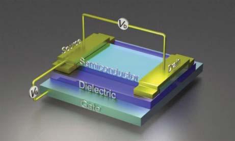
Figure1.1 SchematicillustrationofatypicalOFETarchitecture.
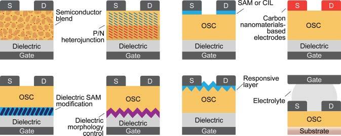
Figure1.2 InterfaceengineeringofinterfacesinOFETs.(a)Interfacewithinthe semiconductorlayers,(b)semiconductor/electrodeinterface,(c)semiconductor/dielectric interface,and(d)semiconductor/environmentinterface.SAM:self-assembledmonolayer; OSC:organicsemiconductor;CIL:chargeinsertionlayer.
devices,acceleratingchargeseparation,andimprovingthedeviceperformance.By designingmixedorsegregatedcrystalheterojunctionsmadeofOSCs,functional devicessuchasphotodetectors,memorydevices,andambipolartransistorscanbe realized.
AnotherimportantinterfaceinOFETsisthesemiconductor/electrodeinterface (Figure1.2b)[9,23–25],whichusuallydeterminestheefficiencyofcharge-carrier injectionandextraction.Bycarefullychoosingtheself-assembledmonolayer(SAM) orchargeinsertionlayer(CIL)tomodifymetalelectrodes,thecharge-injection barriercanbefine-tunedattheinterface,whichcouldsignificantlyreducethecontactresistancebetweensemiconductorsandelectrodes,thusenhancingthedevice performance.Moreinterestingly,byusingfunctionallayers,whosemolecular conformationorelectronicstructurecanbeswitchedbyexternalstimuli,thepropertiesofOFETscanrespondtoexternalsignals.Thisconceptsetsthefoundation forbuildingfunctionaldevicessuchasoptical/electricalswitches,memories,and photodetectors.
Thesemiconductor/dielectricinterfaceisavitalinterface[26,27]thatdominates carriertransport(Figure1.2c)because(i)chargecarriersaregeneratedatthe interfaceand(ii)theelectricalcurrentpathisthroughatmostthefirstfewlayers ofmoleculesattheinterface.Inaddition,thesurfaceenergyandmicrostructure ofthedielectricinterfacehaveasignificantimpactonthelocalmorphologyof thesemiconductorlayer.Therefore,modificationofthisinterfacebySAMsor stimuli-responsivelayersoffersanimportantanduniversalmethodologyto improvethedeviceperformanceandtoevenintegratenewmolecularfunctionalitiessuchasphoto-controllablememories,superconductors,andcharge-trap memoriesintoorganicelectricalcircuits.
Thesemiconductor/environmentinterfaceisusefulforbuildingfunctional OFETsforsensingapplications[12,13,15,17,28–30](Figure1.2d)bydirectly exposingthesemiconductorlayertotheenvironmentbeinganalyzed.Thismethod offerssomevaluableadvantagesoverothertechnologies,suchaslabel-freecapability,real-timedetection,andcompatibilitywithboththebiologicalsystemand theelectronicsindustry.Someintrinsicdrawbacks,however,hampertheuseof OFET-basedsensorsforpracticalsensingapplications.Thefirstisthediffusionof theanalyteintograinboundariesinthesemiconductors,causingeithertrapping ordopingofchargecarriers.Thiscouldresultinseriousproblemssuchasdevice instabilityandirreversibilitybecauseofthephysicallydestructiveinteraction betweensemiconductorsandanalytes.Second,becauseofthesignalamplification characteristicsofOFETs,anynonspecificresponseornoisewouldcauseinterferencewiththeintrinsicsignaloftheanalytes,leadingtoapseudo-signalandpoor selectivity.Therefore,rationalcontrolofinterfacialchargetransportiscrucialto controlthedopingeffects,increasethesensingselectivity/sensitivity,andeven installnewfunctionalities.
1.2BriefHistoricOverviewofInterfaceEngineering inOFETs
WehavesummarizedinFigure1.3thekeydevelopmentstogiveacomprehensivebig pictureoftheinterface-engineeredfunctionalOFETs.Startingfromthefirstdemonstration[31,32]ofOFETsinthe1980stotheirveryrecentapplications[21,29,30]in skinelectronics,theperformanceandfunctionalityofOFETshaveevolvedsimultaneouslyandpromotedeachother,sheddinglightontheirpotentialapplicationsin healthcare,wearableelectronics,anddegradableelectronics.
1.3ScopeoftheBook
Inthiscomprehensive book,weaimtoprovideasystematicsurveyofrecent significantadvancesindevelopingeffectivemethodologiesofinterfaceengineering inOFETs,fromfundamentalmodelstoexperimentaltechniques,forcreating high-performanceandmultifunctionaloptoelectronicdevices.InChapter2,we

Figure1.3 Timelineshowingkeydevelopmentsininterface-engineeredfunctionalOFETs [10,21,25,28,29,31,32,37,57,71,74,77,81,114,137,143–145,160,168,172,180,187, 205,237–240,298,312,315,326,331,333,348,353,359–361,376,393,397,417,447,459].
willsummarizeinterfacialmodificationmethodsinOFETs,whichincludephysical andchemicalmodificationmethods.Wewillnotgointodetailsofthem.Instead, summativetablesandfigureswillbepresenttocompareeachmethod.Then, wefocusonhowtouseinterfaceengineeringstrategiestoimprovetheinherent propertiesofOFETsatthesemiconductor/semiconductorinterface(Chapter3), semiconductor/electrodeinterface(Chapter4),semiconductor/dielectricinterface (Chapter5),semiconductor/environmentinterface(Chapter6),aswellasinterfacingorganicelectronicswithbiology(Chapter7).Bothareofgreatimportanceto liethefoundationoftheOFETresearch.Wealsoprovideacriticaldiscussionof thelimitationsandmainchallengesthatstillexistforthedevelopmentofpractical applicationsinChapter8.Suchabookwillbeinvaluableforbetterunderstanding fundamentalcharge-transportmechanismsattheinterfacesandwilloffernovel insightsintothedevicedesignconcept,thedevicefabricationprocess,andthe developmentoffuturemultifunctionalpracticaltransistors.
InterfacialModificationMethods
Overthepasttwodecades,extensiveefforts[6,8,9,16]havebeendevotedtothe modificationofinterfacesinorganicfield-effecttransistors(OFETs),includingphysicalmodificationmethods,suchasencapsulationorinsertiononthesurface,and chemicalmodificationmethods,suchascovalentlybondedself-assembledmonolayer(SAM)modification.
2.1NoncovalentModificationMethods
2.1.1ChargeInsertionLayerattheElectrodeSurface
BecausetheinjectionbarrieroriginatesgenerallyfromthegapbetweentheFermi levelofmetalelectrodesandthehighestoccupiedmolecularorbital(HOMO)/lowest unoccupiedmolecularorbital(LUMO)energylevelsoforganicsemiconductors (OSCs)accordingtotheenergeticalignment,areasonablesolutionistoinserta suitableadditionallayertomodifytheelectrodeandfunctionasaspringboard forchargecarriers,thuspossiblyovercomingthepoorinjection[70].Initially, thismethodofintroducingathinbufferlayerofseveralnanometersatmetal OSC/electrodeinterfaces,referredtoasachargeinsertionlayer(CIL)[71,72],had alreadybeenappliedtoincreasetheefficiencyoforganiclight-emittingdiodesby improvingthecontact.
Apreliminarystudy[73]wascarriedoutbyHajlaouietal.,whoinsertedathinfilm oftetracyanoquinodimethane(TCNQ)(1),workingasmoleculardopant,between AuandOSCactivelayersinOFETstoachieveanincreasedholemobility.Byusing anultrathinLiFinterlayerasCILbetweenAlelectrodesandF16 CuPcactivelayers [33],enhancedn-channelperformancewasachieved.Sincethen,CILmodification hasattractedmoreandmoreattentionintermsofenhancingthehole/electroninjectionefficiency.Variousmaterials,suchasinorganiccompounds(metaloxidesand inorganicsalts)andorganiccompounds(smallmoleculesandpolymers),havebeen usedasCILs,asshowninFigure2.1.
Metaloxides[74](Figure2.1a)provideavarietyofcandidatesforCILsbecause oftheirwiderangeofworkfunctions.Transitionmetaloxidesinparticular InterfaceEngineeringinOrganicField-EffectTransistors,FirstEdition.XuefengGuoandHongliangChen.
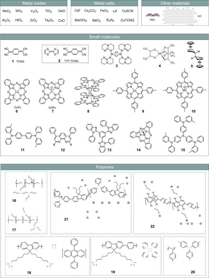
Figure2.1 Chemicalstructuresofthechargeinsertionlayer(CIL).(a)Metaloxides, (b)metalsalts,(c)smallmolecules,(d)polymers,and(e)othermaterials.
[75,76],whoseworkfunctionsrangefromverylow(φ≈ 3eVforZrO2 )toextremely high(φ≈ 7eVforV2 O5 ),aresuitableformodifyingdifferentmetalswithmatched energylevels.AfterintroducingtheCIL,thethicknessofthedepletionlayer betweenthemetalandmetaloxidedecreasestoafewnanometers,producinga reachabledistancefortunnelinginjection,andthecontactresistancecouldbe significantlyreducedoncethetunnelinginjectionisdominant.TheCILlayercan
2.1NoncovalentModificationMethods 9 alsoactasaprotectionlayeragainstthediffusion[77]ofmetalsfromelectrodesor thepermeation[78]ofO2 orH2 Ointotheactivelayer,thusimprovingthedevice stability.
MetalsaltsareanotherbigfamilyofinorganicmaterialsworkingasCILs (Figure2.1b)[79,80].Theyexperienceasimilarmechanismasmetaloxides. OneofthebenefitsofusingmetalsaltsasCILsistheircompatibilitywiththe solution-processmethod.Forexample,CuSCN[81,82]canbespin-castedonAu electrodesasanovelCILwithanintrinsicelectron-blockingproperty.However, therearesomedrawbacksofmetalsaltswhenapplyingthemasCILs.First,the thicknessoftheCILaffectselectrontransport.AthickerlayerofCsF[83](more than0.6nm)decreasedthemobilityowingtoitsinsulatingnature.Second,when depositingaCILintoambipolarOFETsbyusingasinglecomponent,theoutcome performanceofp-andn-channelscannotbeenhancedsimultaneously.This problemcouldbesolvedbymixingtwodifferentmaterialstoformahybridCIL [84].Theinjectionbarrierfordifferenttypesofcarrierswastunedfinelyaccording tothemolecularratioofthetwocompounds.
WhenitcomestoorganicsmallmoleculesasCILs(Figure2.1c),i.e.chargetransfer(CT)complex(2)[85],metalcomplex(3–5)[86,87],metaltetraphenylporphyrinandphthalocyanine(6–10),[88]andN-heterocycliccompounds(11–15) [89],directCToccursattheinterfacebetweentheorganicCILandthesemiconductor,whichhelpstoreducethecontactresistancebytheadditionalinterface dipole.However,aproblemthatstillexistsisthepossibilityofmatrix–dopant hybridization[90,91].Theorganicpolymerswithdipolargroups[23,92,93] (16 and 17)(Figure2.1d)canalsoactaselectrodesurfacemodifierstoachieve electrodeswithalowworkfunction.Polyelectrolytes(18–22),whichcomprisethe groupscapableofbeingchargedwithcationsoranions,wereprovenrecentlytobe apromisingCILtoachieveohmiccontactswithawiderangeofworkfunctions (3.0–5.8eV)[23].
Othermaterials(Figure2.1e),suchasDNA[94]andgrapheneoxides(GOs) [95–97],havealsobeenusedasCILs.Thepresenceofphosphategroupsinthe DNAleadstoadipolelayer,whichcouldchangetheorientationinresponseto appliedgatevoltagesandenhancethechargeinjectionofbothtypesofcarriers. WhenGOswereappliedasCILsinOFETs,theimprovementindeviceperformance couldbeattributedtothegoodcontactnatureofcarbon-basedmaterialswith semiconductors,whichwillbediscussedinSection3.3.2.
2.1.2DielectricSurfacePassivationMethods
Polymerencapsulationisamainchoiceformodifyingtheinorganicdielectric surface.Mostofthepolymermodifier,forexamplepoly(imide-siloxane)[98], poly(4-vinylpyridine)(PVPyr)[99],andpolystyrene(PS)[100],areusedtochange thesurfaceenergyofthedielectricandthusinfluencethegrainsizeofOSCs growingwhereon.Thereisstilladebateonhowthesurfaceenergyofpolymer modifiersinfluenceperformanceofOSCthinfilms;butasageneralrule,thecloser thesurfaceenergyofthedielectriclayeristothatoftheOSC,thehigherthecarrier
2InterfacialModificationMethods
mobility[101].Morefundamentally,itisacompetitionbetweentheaggregation forcewithintheOSCandtheadsorptionofOSConthesubstrate.
Thepolymermodifiers,however,sufferfromhighroughnessandtrapdensity, whichhamperchargetransportonthesurface.Thesameproblemexistswhen directlyusinginsulatingpolymersasgatedielectrics[102–105].Theseapplications callfortheefficientsurfacemodificationmethodsofpolymerfilms.However,the lackoffunctionalgroupsmakesitveryhardtomodifypolymerdielectrics.Several strategieshavebeendevelopedrecentlytosolvethisproblem:
(i)Bydirectlydepositingabilayerdielectricconsistedofabulkdielectriclayerand anultrathininterfacelayer(Figure2.2a,b);
(ii)Byusingblendsoftwocomponentstoinduceaphase-separatedbilayerstructure(Figure2.2c,d);
(iii)Byutilizingamonolayercapableofself-assemblyonthepolymersurface (Figure2.2e–g).
Forthefirststrategy,abilayerpolymerdielectric(Figure2.2a)wasemployed[34], whichconsistedofabulklayerofelectropositivecopolymer(26)forinducingelectrostaticpolarizationalongthechannelandanultrathininterfacelayerof 23 on toptoformagoodinterfacewithOSCs.Thepolymerdielectricwaspreparedvia aone-step,low-temperature,solvent-freechemicalvapordepositionprocesswith differentratiosoftwomonomers 24 and 25 (Figure2.2b)[35].
Thesecondstrategycanberealizedbyblendingafluorinatedhigh-k polymer (27)withpoly(methylmethacrylate)(PMMA)(28)asadielectric[106].Generally, thepurehigh-k dielectriclayerof 27 canenhancetheholemobilitybutsuppress theelectronmobilitybecauseoftheinterfacialC–Fdipole.Intheblends,however, bothp-andn-channelbehaviorswereincreasedsimultaneouslyinambipolarpolymersbecauseoftheexistenceofverticalphaseseparationthatinducesaPMMA-rich regionadjacenttothesemiconductorlayer(Figure2.2c),leadingtoreducedinterfacialdipolardisorder(Figure2.2d).Thesediscoveriesprovidednewstrategiesfor designingdielectricmaterialsbychoosingmultiplecomponentswithproperchemicalandmorphologicalproperties.
Lastbutnotleast,thetechniqueofusingSAMsviacovalentbondingininorganic dielectricscouldnotworkwellonpolymersubstrates,becauseofthelackofparticularanchoringsitesonthepolymersurfacewhosechainsarerandomlyoriented.To overcomethisproblem,Yokotaetal.[108]appliedaparticularparaffinictriptycene (29)(Figure2.2f),whichcanformcompletelyorientedthinfilmswithahigh structuralorderfeaturing2Dnestedhexagonalpackingand1Dlayerstackingfor thesurfacefunctionalizationofapolymersubstrate.Thetriptyceneformednoncovalentlyonpolymersubstrates,wheretheparaffinicsidechainswerearranged verticallytothesubstrate,thusequalizingthesurfacepropertiesofthesesubstrates (Figure2.2e)[107].Withafew-layertriptycenefilm,thesurfaceenergiesofdifferentgatedielectricswerealmostidentical(∼22.2mJm 2 ),thusensuringthehigh crystallinityandenhancedstructuralintegrityofOSCs(Figure2.2g).Thisisamore generalstrategybydepositingafew-layerfilmoftriptyceneonpolymersubstrates, sheddingnewlightoninterfaceengineeringoftheOSC/polymerdielectricinterface.