About the Editors

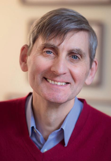
Arokia Nathan is a leading pioneer in the development and application of thin film transistor technologies to flexible electronics, display and sensor systems. His current research interests lie in integration of devices, circuits, and systems using a broad range of inorganic and organic thin film material systems on rigid and mechanically flexible substrates for large area systems. Following his PhD in Electrical Engineering, University of Alberta, Canada in 1988, he joined LSI Logic Corp., Santa Clara, CA, where he worked on advanced multichip packaging techniques and related issues. Subsequently he was at the Institute of Quantum Electronics, ETH Zürich, Switzerland, before joining the Electrical technology and was a recipient of the 2001 Natural Sciences and Engineering Research Council E.W.R. Steacie Fellowship. In 2004, he was awarded the Canada Research Chair in nano-scale flexible circuits. In 2005/2006, he was a visiting professor in the Engineering Department, University of Cambridge, UK. Later in 2006, he joined the London Centre for Nanotechnology, University College London as the Sumitomo Chair of Nanotechnology. He moved to Cambridge University in 2011 as the Chair of Photonic Systems and Displays, and he is currently a Bye-Fellow and Tutor at Darwin College. He has over 600 publications in the field of sensor technology and CAD, and thin film transistor electronics including 6 books, and more than 130 patents and four spin-off companies. He is a recipient of the Royal Society Wolfson Research Merit Award, the BOE Award for contributions to TFT CAD, and winner of the 2020 IEEE EDS JJ Ebers Award. He serves on technical committees of professional societies and conferences in various capacities. He is currently the vice president of Publications and Products in IEEE’s Electron Devices Society. He is a fellow of IEEE, a Distinguished Lecturer of the IEEE Electron Devices Society and Sensor Council, a chartered engineer (UK), Fellow of the Institution of Engineering and Technology (UK), Fellow of the Royal Academy of Engineering, of the Society for Information Displays, and Fellow of the Canadian Academy of Engineering.

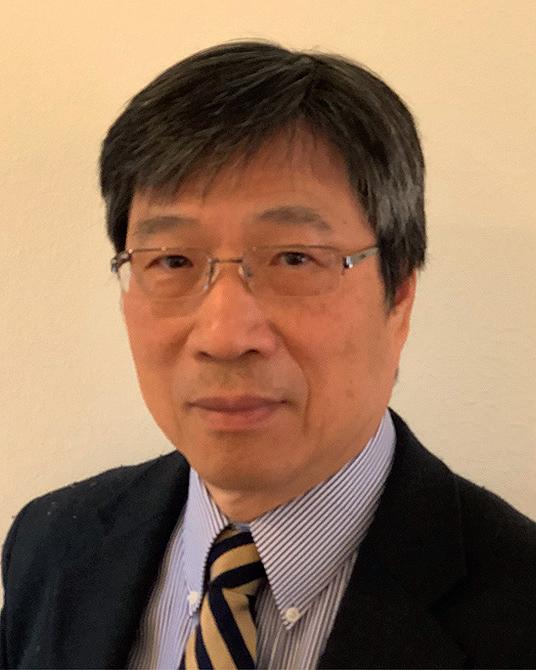
Samar K. Saha is the Chief Research Scientist at Prospicient Devices, Milpitas, California, USA. Since 1984, he has worked at various technical and management positions for SuVolta, Silterra USA, DSM Solutions, Synopsys, Silicon Storage Technology, Philips Semiconductors, LSI Logic, Texas Instruments, and National Semiconductor. He has, also, worked as an Electrical Engineering faculty at Santa Clara University, California; the University of Colorado at Colorado Springs, Colorado; the University of Nevada at Las Vegas, Nevada; Auburn University, Alabama; and Southern Illinois University at Carbondale, Illinois. He has authored over 100 research papers; two books entitled, FinFET Devices for VLSI Circuits and Systems (CRC Press, 2020) and Compact Models for Integrated Circuit Design: Conventional Transistors and Beyond (CRC Press, 2015); one book chapter, “Introduction to Technology Computer Aided Design,” in Technology computer Aided design: Simulation for VLSI MOSFET (C.K. Sarkar, ed., CRC Press, 2013); and holds 13 US patents. His book on FinFET has been translated into Chinese language entitled, Nanoscale Integrated Circuits FinFET Device Physics and Modeling (CRC Press/China Machine Press, 2022).
Dr. Saha served as the 2016–2017 President of the Institute of Electrical and Electronics Engineers (IEEE) Electron Devices Society (EDS) and currently serving as a member of the IEEE Fellow Committee. He is a life fellow of IEEE, a fellow of the Institution of Engineering and Technology (IET), UK, and a distinguished lecturer of IEEE EDS. Previously, he has served EDS as senior past and junior past president; Awards chair; vice president of publications; an elected member of the Board of Governors; fellow evaluation committee chair; editor-in-chief of IEEE QuestEDS; chair of George Smith and Paul Rappaport awards; editor of Region-5 and 6 Newsletter; chair of Compact Modeling Technical Committee; and Chair of North America West Subcommittee for Regions/Chapters; IEEE as a member of the Conference Publications Committee and TAB Periodicals Committee; and Santa Clara Valley/San Francisco EDS chapter as the treasurer, vice chair, and chair.
In publications, he has served as a Guest Editor of six Special Issues (SIs) of IEEE EDS journals including head guest editor of the IEEE Transactions on Electron Devices SIs on Advanced Compact Models and 45-nm Modeling Challenges and Compact Interconnect Models for Giga Scale Integration and two IEEE Journal of Electron Devices Society SIs from the selected extended papers presented at conferences. Dr. Saha received the PhD degree in Physics from Gauhati University, India, and MS degree in Engineering Management from Stanford University, USA. He is the recipient of the 2021 IEEE EDS Distinguished Service Award.

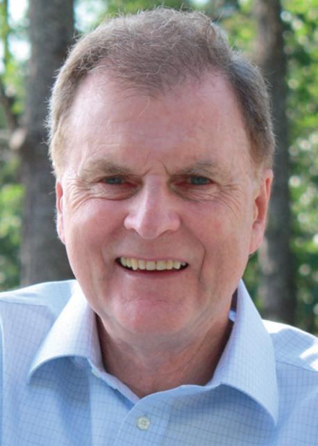
Ravi M. Todi received his Masters and Doctoral degrees in Electrical Engineering from University of Central Florida (UCF), Orlando, Florida. His graduate research was focused on gate stack engineering, with emphasis on binary metal alloys as gate electrode and on highmobility germanium channel devices. In his early career, as advisory engineer/scientist at semiconductor research and development center (SRDC) at IBM microelectronics division, his work was focused on high-performance embedded dynamic random-access memory (eDRAM) integration on 45 nm silicon on insulator (SOI) logic platform. For his many contributions to the success of the eDRAM program at IBM, Ravi was awarded IBM’s prestigious outstanding technical achievement award. Over the past decade, Ravi has held several lead technical and management positions at Qualcomm, GlobalFoundries, and Western Digital. Most recently he is the silicon technologist responsible for foundry technology at an early-stage Silicon Valley startup. With over 60 US granted patents, over 30 peer-reviewed journal publications, over 40 international conference presentations, and over 50 invited distinguished lectures, Ravi is well known in the semiconductor industry as a technical/business leader.
Ravi served as an associate editor for IEEE Transactions on Electron Devices from 2014 to 2019, as IEEE-EDS treasurer from 2012 to 2015, as IEEE-EDS vice president for technical activities and conferences from 2016 to 2019, as EDS president-elect in 2020, and is currently serving as EDS president from 2021 to 2023. He is the recipient of 2011 IEEE EDS Early Career Award. He is an IEEE Fellow and is a Distinguished Lecturer for IEEE Electron Devices Society.
About the Authors
Chapter 1
Leo Esaki was born in Osaka, Japan, in 1925. He received his BS and PhD degrees in physics in 1947 and 1959, respectively, from the University of Tokyo, Japan. He was an IBM Fellow and engaged in semiconductor research at the IBM Thomas J. Watson Research Center, Yorktown Heights, New York, from 1960 to 1992. Prior to joining IBM, he worked at Sony Corp., where his research on heavily doped Ge and Si resulted in the discovery of the Esaki tunnel diode; this device constitutes the first quantum electron device. Since 1969, Esaki has, with his colleagues, pioneered “designed semiconductor quantum structures” such as man-made superlattices, exploring a new quantum regime at the frontier of semiconductor physics. He also served as President of the University of Tsukuba (1992–1998) and Shibaura Institute of Technology (2000–2005). Since April 2006, he has assumed the position of president of the Yokohama College of Pharmacy.
Dr. Esaki was awarded the 1973 Nobel Prize in Physics in recognition of his pioneering work on electron tunneling in solids. He is also a recipient of the Nishina Memorial Award, the Asahi Press Award, the Toyo Rayon Foundation Award, the IRE Morris N. Liebmann Memorial Prize, the Franklin Institute’s Stuart Ballantine Medal, the Japan Academy Award, the Order of Culture from the Japanese Government, the American Physical Society International Prize for New Materials, the IEEE Medal of Honor, the Japan Prize, and the Grand Cordon of the Order of the Rising Sun, First Class from the Japanese Government.
He is a Fellow of the American Academy of Arts and Sciences, a member of the Japan Academy, a Foreign Associate of the National Academy of Science and the National Academy of Engineering, a member of the Max-Planck-Gesellschaft, and a foreign member of the American Philosophical Society, the Russian Academy of Sciences, and the Italian National Academy of Science.
Chapter 2
Dr. Samar K. Saha has served as the 2016–2017 President of the IEEE Electron Devices Society (EDS). Currently, he is the Chief Scientist at Prospicient Devices, Milpitas, USA. Since 1984, he has worked in various technical/management positions at National Semiconductor, LSI Logic, Texas Instruments, Philips Semiconductors, Silicon Storage Technology, Synopsys, DSM Solutions, Silterra USA, and SuVolta. In academia, he was an Electrical Engineering faculty at Southern Illinois University at Carbondale, Illinois; Auburn University, Alabama; the University of Nevada at Las Vegas, Nevada; the University of Colorado at Colorado Springs, Colorado; and Santa Clara University, Santa Clara, USA.
He has authored over 100 research papers; two books entitled, FinFET Devices for VLSI Circuits and Systems (CRC Press, 2020) and Compact Models for Integrated Circuit Design: Conventional Transistors and Beyond (CRC Press, 2015); one book chapter, “Introduction to Technology Computer Aided Design,” in Technology
computer Aided design: Simulation for VLSI MOSFET (C.K. Sarkar (ed.), CRC Press, 2013); and holds 13 US patents. His book on FinFET has been translated in Chinese language entitled, Nanoscale Integrated Circuits FinFET Device Physics and Modeling (CRC Press/China Machine Press, 2022).
Dr. Saha received the PhD degree in Physics from Gauhati University and an MS degree in Engineering Management from Stanford University. He is a distinguished Lecturer of IEEE EDS, an IEEE Life Fellow, and a Fellow of the Institution of Engineering and Technology (IET), UK. He is the recipient of 2021 IEEE EDS Distinguished Service Award.
Chapter 3

Prasanta Kumar Basu (MIEEE’04-SMIEEE’09) was born in 1946 and obtained BSc (Physics honors), and BTech and MTech. degrees in Radio Physics and Electronics, all from the University of Calcutta (CU). He joined the Institute of Radio Physics and Electronics, CU (IRPE-CU) as a lecturer in 1971 and retired as professor from there in 2011. He then worked as UGC BSR Faculty Fellow, and afterward as visiting Professors at IIT Kharagpur and National Chung Cheng University, Taiwan. He did research in physics of semiconductors and their nanostructures, and electronic and photonic devices. He has authored more than 140 journal papers, many refereed conference papers, and three book chapters. He has authored and coauthored four books: Theory of Optical Processes in Semiconductors (Oxford University Press, UK, 1997), Silicon Photonics (with M J Deen, Wiley, UK, 2012), Semiconductor Laser Theory (with Bratati Mukhopadhyay and Rikmantra Basu; CRC Press, USA, 2015), and Semiconductor Nanophotonics (with Bratati Mukhopadhyay and Rikmantra Basu; Oxford University Press, UK, 2022). He visited Germany as an Alexander von Humboldt Fellow, and McMaster University, Canada, several times as a visiting professor. He also visited the United States, the United Kingdom, and several European and Asian countries as a visiting professor, researchers, and authors of papers in conferences. Currently, he is engaged in collaborative research and book writing with faculties of IRPE-CU and NIT Delhi. He writes and gives lectures on topics related to history of science and technology and recent developments in electronics and photonics.
Chapter 4
Robert B. Kaufman is a PhD candidate at the University of Illinois Urbana-Champaign in the department of Electrical and Computer Engineering. He received a BS and MS in electrical engineering from the University of Illinois Urbana-Champaign in 2017 and 2021, respectively. His research is in the field of optoelectronics under the advisement of Prof. John Dallesasse. Specifically, Robert has been focused on the design, fabrication, and characterization of a novel variation of the quantum- cascade laser that incorporates a heterojunction bipolar transistor. He is a student member of IEEE.

John M. Dallesasse is a Professor of Electrical and Computer Engineering and Associate Dean in the Grainger College of Engineering at the University of Illinois at Urbana-Champaign (UIUC), where he has been for over 11 years. He also has over 20 years of industry experience in technology development and executive management, having led technically diverse and geographically distributed engineering teams. Prior to joining UIUC, he was the Chief Technology Officer, Vice President, and cofounder of Skorpios Technologies, where he was responsible for developing innovative methods for heterogeneous integration of compound semiconductors with silicon. His technical contributions include, with Nick Holonyak, Jr., the discovery of III–V Oxidation, which has become an enabling process technology for the fabrication of Vertical-Cavity Surface-Emitting Lasers (VCSELs) for optical networking, 3D imaging, and LIDAR applications. His research group at UIUC works on novel methods for heterogeneous integration using epitaxial transfer which have been applied to the fabrication of VCSELs and other photonic devices on silicon, on mode control methods which have been used to provide record single-mode powers on conventional VCSEL structures, and on mid-IR emitters using quantum cascade structures within a transistor structure. John has over 100 publications and conference presentations, and 51 issued patents. He serves or has served as the Chair of the Steering Committee for the IEEE Journal of Lightwave Technology, the Chair of the Steering Committee for the IEEE Transactions on Semiconductor Manufacturing, and as the Vice President of Technical Committees for IEEE-EDS. He is a Fellow of the IEEE and Optica.
Chapter 5
Chapter 6
Tak H. Ning received his PhD degree in physics from the University of Illinois at Urbana-Champaign in 1971. He joined IBM Thomas J. Watson Research Center in 1973, working there until retirement, as an IBM Fellow, in 2016. He made significant contributions to the understanding of hot-electron effects in MOSFETs, and to advancing the technologies of bipolar transistors, CMOS and EEPROM. He has received several awards, including the 2007 Electrochemical Society Gordon E. Moore Medal, the 1989 IEEE Electron Devices Society J. J. Ebers Award, and the 1991 IEEE Jack A. Morton Award. He is a member of the U.S. National Academy of Engineering, and a fellow of the IEEE and of the American Physical Society.
Mamidala Jagadesh Kumar (SMIEEE’98) is a Professor (on-leave) at the Indian Institute of Technology, New Delhi, India. He was the ViceChancellor of Jawaharlal Nehru University, New Delhi, India. He is currently the Chairman, University Grants Commission, and Chairman, All India Council for Technical Education, Government of India. He is the Editor-in-Chief of IETE Technical Review and an Editor of IEEE Journal of the Electron Devices Society. He was an Editor of IEEE Transactions on Electron Devices from 2006 to 2015. He has widely published in the area of Micro/Nanoelectronics and is known for his excellence in teaching. He has coauthored three books and one
of them is on “Junctionless Field Effect Transistors: Design, Modeling and Simulation” which is published by the Wiley-IEEE press.

Shubham Sahay (MIEEE’15) is an assistant professor in the department of Electrical Engineering at Indian Institute of Technology (IIT) Kanpur, India. Prior to joining IIT Kanpur, he worked as a postdoctoral research scholar at the University of California, Santa Barbara (2018–2020). He received the BTech (Hons.) in Electronics Engineering with four gold medals and several cash prizes from the IIT BHU Varanasi in 2014 and the PhD degree in Electrical Engineering from IIT Delhi in 2018. He has coauthored a book on “Junctionless Field Effect Transistors: Design, Modeling and Simulation” which is published by the Wiley-IEEE press. He has also published several peer-reviewed articles on topics including semiconductor device design and modeling, neuromorphic computing, and hardware security primitives utilizing emerging nonvolatile memories. He is an editor of IETE Technical Review and review editor for Frontiers in Neuroscience: Neuromorphic Engineering and Frontiers in Electronics: Integrated Circuits and VLSI. He is a member of IEEE and the chair of IEEE EDS UP section. He also appeared in the list of Golden reviewers for IEEE Transactions on Electron Devices and IEEE Electron Device Letters from 2016 to 2022. His present research interests include Hardware Neuromorphic computing platforms, Hardware security primitives, Novel Device Architectures for Sub-10 nm Regime, Analytical and Compact Modeling of Semiconductor Devices and Nonvolatile Memories, and Spintronics.
Chapter 7

Hiroshi Iwai is a semiconductor device engineer, who contributed to the development of integrated circuits technologies and products. He received BE and Doctor Degree in Engineering from the University of Tokyo. He worked at Toshiba, Tokyo Institute of Technology, and National Yang Ming Chiao Tung University for 50 years since 1973. Especially, he has contributed to the miniaturization of the LSIs since the 8 μm PMOS generation. He developed Toshiba’s first NMOS LSI technology in 1975, as well as 1k bit SRAMs. For the development of a 64 k bit DRAM, he introduced stepper lithography and dry process into production for the first time in the world in 1980. He broke the 0.1 μm limit of CMOS miniaturization by developing 40 nm MOSFET technologies in 1993, which was more than 2 generations earlier than competitive companies. He developed the world’s first 0.15 μm RFCMOS technologies in the middle of 1990s, which contributed to the realization of Bluetooth. Dr. Iwai has contributed to IEEE and EDS activities and administrations over 40 years. He served as the IEEE EDS president and the IEEE Division I director. He was appointed to the first IEEE EDS eminent lecturer. Currently, he is a vice dean and a distinguished chair professor of National Yang Ming Chiao Tung University and a professor emeritus of Tokyo Institute of Technology.
Chapter 8
Robert E. Kerwin is currently an independent consultant in electronics technology, intellectual property management, and quality management practices. In April 1994, he retired from AT&T as a General Manager of the Intellectual Property Division. Prior to that, he had been Manager, Corporate Quality at AT&T after 22 years of experience at AT&T Bell Laboratories.
At AT&T Bell Laboratories, Dr. Kerwin was a member of Technical Staff in the Electronic Component Processes Laboratory (1964–1971), supervised the Photolithography Development Group (1971–1974), supervised the Murray Hill Integrated Circuit Design Capability Line responsible for the development of CMOS processing technology (1974–1980), and headed the Component Quality and Reliability Department responsible for reliability assurance of all electronic components made by or purchased for AT&T (1980–1986).
Dr. Kerwin holds a BS degree in Chemistry from Boston College, an MS degree in Chemistry from the Massachusetts Institute of Technology, and a PhD degree in Chemistry from the University of Pittsburgh. Prior to joining AT&T Bell Laboratories, he was a Research Fellow in the Polymer Studies Group at the Mellon Institute.
He is a Bell Laboratories Fellow, a Fellow of the American Institute of Chemistry, a member of the Society of Sigma Xi, the American Association for the Advancement of Science, and the Institute Electrical and Electronics Engineers. In 1994, he received the Jack A. Morton Award from the IEEE “For Outstanding Contributions in the Field of Solid State Devices,” and Inventor of the Year Award from the New Jersey Inventors Hall of Fame.
He holds 15 patents on microelectronics materials and processes, including the fundamental silicongate process used in all semiconductor memory and microprocessor devices. He has published 15 papers and 5 book chapters on microelectronics technology, quality management principles, and intellectual property management.
Dr. Kerwin served as a member of the Board of Examiners for the Malcolm Baldridge National Quality Award (1988–1991), and lectured on quality management practices at the Brookings Institution (1986–1991).
Chapter 9

Alfred U. MacRae was born in New York City in 1932. He earned his bachelor’s and graduate degrees at Syracuse University, where he studied physics. Upon completing his doctorate in 1960, MacRae began working for Bell Telephone Laboratories, first in Murray Hill and then in Holmdel, New Jersey. He researched the location of atoms on metals and semiconductors, worked on ion implantation, worked on the fabrication, design, and testing of integrated circuits, and finally led an organization that developed large transmission systems and satellite communications. He retired in 1995 as Director of the Satellite Communications Lab. He held 18 patents and was published in numerous technical journals. MacRae was elected a fellow of the American Physical Society in 1964, was the 1994 recipient of the J.J. Ebers Award, presented by the IEEE Electron Devices Society, and was elected to membership of the National Academy of Engineering in 2003. MacRae passed away at home in Seattle, Washington, in early 2023.
Chapter 10
Yuan Taur received the BS degree in physics from National Taiwan University, Taipei, Taiwan, in 1967 and the PhD degree in physics from the University of California, Berkeley, in 1974.
From 1979 to 1981, he worked at Rockwell International Science Center, Thousand Oaks, California, on II–VI semiconductor devices for infrared sensor applications. From 1981 to 2001, he was with the Silicon Technology Department of IBM Thomas J. Watson Research Center, Yorktown Heights, New York, where he was the Manager of Exploratory Devices and Processes. Since October 2001, he has been a professor in the Department of Electrical and Computer Engineering, University of California, San Diego. He became a Distinguished Professor in 2014.
Dr. Yuan Taur was elected a Fellow of the IEEE in 1998. He has served as the Editor-in-Chief of the IEEE Electron Device Letters from 1999 to 2011. He has also served on the technical program committees and as a panelist for the Device Research Conference, and the International Electron Devices Meeting, and as the Program Chairman for the Symposium on VLSI Technology.
Dr. Yuan Taur has authored or coauthored over 200 technical papers and holds 14 U.S. patents. He coauthored a book, “Fundamentals of Modern VLSI Devices,” published by Cambridge University Press in 1998. The 2nd edition was published in 2009, the 3rd edition in 2022.
Dr. Yuan Taur received the IEEE Electron Devices Society’s J.J. Ebers Award in 2012 “for contributions to the advancement of several generations of CMOS process technologies.” He also received the IEEE Electron Devices Society’s Distinguished Service Award in 2014.
Chapter 11

Sorin Cristoloveanu received the PhD (1976) in Electronics and the French Doctorat ès-Sciences in Physics (1981) from Grenoble Polytechnic Institute, France. He is currently an Emeritus Director of Research CNRS. He also worked at JPL (Pasadena), Motorola (Phoenix), and the Universities of Maryland, Florida, Vanderbilt, Western Australia, Kyungpook (World Class University project, Korea), and Nanjing. He served as the director of LPCS Laboratory and Center for Advanced Projects in Microelectronics, initial seed of Minatec center. He has authored more than 1100 technical journal papers and communications at international conferences (including 170 invited contributions). He is the author or the editor of 36 books, and he has organized 35 international conferences. His expertise is in the area of the electrical characterization and modeling of semiconductor materials and devices, with special interest for silicon-on-insulator structures. He has supervised more than 110 PhD completions. With his students, he has received 17 Best Paper Awards, an Academy of Science Award (1995), and the Electronics Division Award of the Electrochemical Society (2002). He is a Life Fellow of IEEE, a Fellow of the Electrochemical Society, Doctor Honoris Causa of the University of Granada, and Editor of SolidState Electronics. He is the recipient of the IEEE Andy Grove award 2017, the most prestigious distinction in the field of electronic components, for contributions to “silicon-on-insulator technology and thin body devices.” This is actually the topic of his recent book, https://www.sciencedirect.com/book/ 9780128196434/fully-depleted-silicon-on-insulator#book-info.
Chapter 12
Professor Chenming Hu is an electronics innovator, TSMC Distinguished Professor Emeritus at the University of California, Berkeley, and renowned internationally as the Father of the 3D Transistor FinFET. Intel called FinFET the most radical shift in semiconductor technology in over 50 years in 2011. Today, all advanced computers, servers, and smartphones are using 3D transistor processors.
Hu also led and continues to lead the development of the BSIM suite of transistor standard models that the IC industry has used to design ICs with cumulative worth over a trillion US dollars since 1996.
He has served as the Chief Technology Officer of TSMC (Taiwan Semiconductor Manufacturing Company) and Chairman of the nonprofit East Bay Chinese School and Friends of Children with Special Needs.
Professor Hu was honored with UC Berkeley’s highest honor for teaching in 1997, the highest medal of the Institute of Electrical and Electronic Engineers in 2020, and memberships in the US National Academy of Engineering, the Chinese Academy of Sciences, the US Academy of Inventors, and Academia Sinica of Taiwan. He has received PhD degree from UC Berkeley and honorary doctoral degrees from Hong Kong University and NYCU. He has authored five books and 1000 research papers and has been granted over 100 US patents.
In 2016, Professor Hu was presented with the National Medal of Technology and Innovation by President Obama in the White House.
Chapter 13
Digh Hisamoto received the BS, MS, and PhD degrees from the University of Tokyo in 1984, 1986, and 2003, respectively.
In 1986, he joined Central Research Laboratory, Hitachi, Ltd., Tokyo, where he has been working on ULSI device physics and process technologies. He developed scaled CMOS and memory devices including DELTA, the original model of FinFET. From 1997 to 1998, he was a Visiting Industrial Fellow at the University of California, Berkeley, where he developed the first FinFET. For this achievement, he received the IEEE Andrew S. Grove Award in 2019. He has expanded his research interests into RF devices, tunnel FETs, Nonvolatile memory devices, and Power devices using wide bandgap semiconductors.
From 2015 to 2019, he was an invited visiting professor at the Tokyo Institute of Technology, where he started the research of quantum devices including quantum sensors with color centers of wide bandgap materials and Si quantum computing devices.
He served as a member of the Committee of International Electron Devices Meeting, VLSI Symposium and International Conference on Solid State Devices and Materials, and an Associate Editor of IEEE Electron Device Letters. He also served as an Executive Director of the Japan Society of Applied Physics (JSAP).
Dr. Hisamoto is Fellow of the IEEE and JSAP.
Chapter 14

Gehan A. J. Amaratunga obtained his BSc and PhD in Electrical Engineering from the Universities of Cardiff and Cambridge, respectively. He has been the 1966 Chair Professor in Engineering at the University of Cambridge since 1998. Previously, he was Assistant and Associate Professor at the University of Southampton (1984–1987), Associate Professor at the University of Cambridge (1987–1995), and Chair Professor in Electrical Engineering at the University of Liverpool (1995–1998). He spent a sabbatical year (1989) at Stanford University on a Royal Academy of Engineering Global Research Award. His broad areas of research interests are in Electrical/Electronic Engineering, Applied Physics, and related materials. He with his group have made what can be termed milestone contributions in the areas of power electronic devices and carbon materials, including amorphous carbon and nanotubes, for electronics. From this research, he also proposed and demonstrated the MOS Tunnel FET, carbon nanotube–polymer composite photovoltaic cells, and ultralow threshold thin film field emission cathodes. More recently he has developed new concepts for energy-efficient full color lighting based on quantum dots.
Professor Amaratunga has also been a founder of six start-up companies, three of which successfully introduced new products into the market and were acquired. He is a Fellow of the Royal Academy of Engineering UK (RAEng). He was elected a Fellow Royal Society of Arts UK and awarded the Silver Medal of the RAEng in recognition of his contributions to technical innovations which have resulted in commercial success.
Chapter 15
Dr. Simon M. Sze received his BS degree from the National Taiwan University in 1957, MS from the University of Washington in 1960, and PhD from Stanford University in 1963, all in Electrical Engineering. He was a member of the Technical Staff at Bell Laboratories in Murray Hill, NJ, from 1963 to 1989 and a Distinguished Chair Professor at the National Chiao Tung University (NCTU), Taiwan, from 1990 to 2006. Currently, he is an Honorary Chair Professor at NCTU. In the past, he has served as a Visiting Professor at Cambridge University, Delft University, Soochow University, Stanford University, Swiss Federal Institute of Technology, and Tokyo Institute of Technology.
Simon has made fundamental and pioneering contributions to semiconductor devices, especially the metal–semiconductor contacts, microwave devices, and MOSFET technology. Of particular importance is his ground-breaking co-invention of the floating-gate memory (FGM) effect with Dr. Dawon Kahng which has subsequently given rise to a large family of memory devices including EPROM, EEPROM, and Flash memory.
He has authored or coauthored over 350 technical papers and authored/coauthored and edited 16 books. His book “Physics of Semiconductor Devices” (Wiley, 1969; 2nd Ed, 1981; 3rd Ed, with Dr. K.K. Ng, 2007) is one of the most cited works in contemporary engineering and applied science publications (over 47,500 citations according to Google Scholar). He has received the IEEE J.J. Ebers Award, the National Endowed Chair Professor Award, the Flash Memory Summit Lifetime Achievement Award, and the National Science and Technology Prize. He is an EDS Celebrated member, Life Fellow
of IEEE, an ITRI Laureate, an Academician of the Academia Sinica, a foreign member of the Chinese Academy of Engineering, and a member of the US National Academy of Engineering.
Chapter 16

Stefan K. Lai received his BS in applied physics from California Institute of Technology, and his PhD in applied quantum physics from Yale University. From Yale, Lai joined IBM Yorktown TJ Watson Research Center as a Member of Technical Staff, where he conducted research on silicon/silicon-dioxide interface properties. Lai joined Intel in 1982 to develop scalable EEPROM and he coinvented the EPROM tunnel oxide (ETOX) flash memory cell, which has become industry standard. In 1999, he started a team to develop alternative memory technologies and Intel was one of first major semiconductor company to pursue phase change memory (PCM). He was appointed Vice President of Intel’s Technology and Manufacturing Group in 2000. He retired from Intel at the end of 2006. From February 2007 to July of 2008, he was Vice President, Business Development, Ovonyx Inc., a PCM company. He is currently retired. Lai was recognized as an IEEE Fellow in 1998 for his research on the properties of silicon MOS interfaces and the development of flash EPROM memory. He has also been awarded the 2008 IEEE Andrew Grove Award for his contribution to flash memories.
Chapter 17

Mitsumasa Koyanagi was born in Hokkaido, Japan, in 1947. He received the PhD degree in electronic engineering from Tohoku University in 1974 and then joined Hitachi Ltd., where he worked on research and development of MOS memory device and process technology and invented a stacked capacitor DRAM memory cell which has been widely used in the DRAM production. In 1985, he joined the Xerox Palo Alto Research Center, where he worked on research and development of submicron CMOS devices and the design of analog/digital LSIs. In 1988, he joined Hiroshima University, where he worked on sub-0.1 μm MOS devices, 3D integration technology, and optical interconnection. Since 1994, he has been a professor in Tohoku University, where his interests were 3D integration technology, optical interconnection, nano-CMOS devices, memory devices, parallel computer system, artificial retina chip and retinal prosthesis chip, brain–machine interface (BMI), and neural prosthesis chip. He proposed 3D integration technology using TSV in 1989 and fabricated 3D stacked image sensor chip in 1999, 3D stacked DRAM chip in 2000 and 3D stacked microprocessor chip in 2002 for the first time in the world which have been currently commercialized by semiconductor companies. He established a small production line for 3D integration using 12-in. wafers called GINTI (Global Integration Initiative) in 2013 and became a director. Currently, he is a senior research fellow in New Industry Creation Hatchery Center (NICHe), Tohoku University. He has published more than 400 technical papers and given more than 200 invited talks. He was awarded IEEE Jun-ichi Nishizawa Medal, IEEE Cledo Brunetti Award, IEEE EPS Award, the National Medal Order of the Sacred Treasure, the National Medal with Purple Ribbon, the Award of Ministry of Education, Culture, Sports, Science and Technology in Japan, and so on. He is an IEEE life fellow and a JSAP fellow.
Chapter 18

Subramanian S. Iyer (Subu) is Distinguished Professor and holds the Charles P. Reames Endowed Chair in the Electrical Engineering Department and a joint appointment in the Materials Science and Engineering Department at the University of California at Los Angeles. He is Director of the Center for Heterogeneous Integration and Performance Scaling (UCLA CHIPS). Prior to that, he was an IBM Fellow. His key technical contributions have been the development of the world’s first SiGe-based HBT, Salicide, electrical fuses, embedded DRAM, and 45 nm technology node used to make the first generation of truly low-power portable devices as well as the first commercial interposer and 3D integrated products. He also was among the first to commercialize bonded SOI for CMOS applications through a start-up called SiBond LLC. More recently, he has been exploring new packaging paradigms and device innovations that may enable wafer-scale architectures, in-memory analog computer, and medical engineering applications. He has published over 300 papers and holds over 75 patents. He has received several outstanding technical achievements and corporate awards at IBM. He is an IEEE Fellow, an APS Fellow, an iMAPS Fellow, a Distinguished Lecturer of the IEEE EDS and EPS, and a member of the Board of Governors of IEEE EPS. He is also a Fellow of the National Academy of Inventors. He is a Distinguished Alumnus of IIT Bombay and received the IEEE Daniel Noble Medal for emerging technologies in 2012 and the 2020 iMAPS Daniel C. Hughes Jr Memorial award and the iMAPS distinguished educator award in 2021.

John D. Cressler received his BS from Georgia Tech in 1984 and his PhD from Columbia University in 1990. From 1984 to 1992, he was on the research staff of the IBM T.J. Watson Research Center, and from 1992 to 2002, he served on the faculty of Auburn University. In 2002, he joined the faculty at Georgia Tech, and is currently Regents Professor and Schlumberger Chair Professor in Electronics in the School of Electrical and Computer Engineering. Over his 30-year academic career, Cressler’s research has centered on Si/SiGe electronic and photonic devices and circuits. He and his students have published over 800 scientific papers in this field, and he has graduated 71 PhD students to date. He was elected IEEE Fellow in 2001, was awarded the 2010 Class of 1940 W. Howard Ector Outstanding Teacher Award (Georgia Tech’s top teaching award), the 2011 IEEE Leon Kirchmayer Graduate Teaching Award (the IEEE’s top graduate teaching award), the 2013 Class of 1934 Distinguished Professor Award (the highest honor Georgia Tech bestows on its faculty), and the 2021 IEEE James H. Mulligan, Jr. Education Medal (the highest award IEEE gives in teaching and mentoring). He has served the IEEE Electron Devices and Solid-State Circuits Societies in multiple roles, including as Editor-in-Chief of IEEE Transactions on Electron Devices, from 2012 to 2015. Cressler’s books include Silicon-Germanium Heterojunction Bipolar Transistors, The Silicon Heterostructure Handbook, Silicon Earth: Introduction to Microelectronics and Nanotechnology, Extreme Environment Electronics, and four historical novels, all love stories set in medieval Muslim Spain.
Chapter 19
Colombo R. Bolognesi (Fellow, IEEE) was born in St-Lambert QC, Canada. He earned the PhD (EE) from UCSB in 1993. In 1994, he was with Nortel in Ottawa as a BiCMOS Process Integration Engineer for high-speed submicron polysilicon emitter BJTs. He joined Simon Fraser University in 1995, and initiated research on InP/GaAsSb DHBTs in 1996. In 2001, his team demonstrated the first transistors with fT /fMAX cutoff frequencies exceeding 300 GHz with a 6 V breakdown, and a process was transferred to HP (in production at Agilent/Keysight in 2004).
In 2006, he took the Millimeter-Wave Electronics Chair at ETHZürich where DHBT work continued, yielding the highest oscillation frequency in a bipolar transistor (2021). With III–V Lab, InP/GaAsSb DHBTs were used to demonstrate >200 Gb s−1 mixed-mode circuits with record output voltage swings in 2022.
He initiated the development of mm- wave GaN HEMTs in 2007: his Group first achieved 200 GHz cutoff frequencies on SiC substrates, and demonstrated the suitability of GaN- on- Si up to 100 GHz.
His ETH Group also developed InP HEMTs exploited in the European Space Agency Deep Space Network to support missions around Mars, Jupiter, Mercury, and the mapping of dark matter in the Universe. DIRAMICS, an ETH start- up, commercializes the HEMT technology internationally.
Chapter 20
Jesús A. del Alamo is the Donner Professor and Professor of Electrical Engineering at Massachusetts Institute of Technology. He obtained a Telecommunications Engineer degree from Polytechnic University of Madrid and MS and PhD degrees in Electrical Engineering from Stanford University. In 1985, he joined Nippon Telegraph and Telephone LSI Laboratories in Japan and since 1988 he has been with the Department of Electrical Engineering and Computer Science of Massachusetts Institute of Technology. From 2013 until 2019, he served as Director of the Microsystems Technology Laboratories at MIT. His current research interests are focused on nanoelectronics based on compound semiconductors and ultrawide bandgap semiconductors as well as novel ionic and ferroelectric devices for artificial intelligence accelerators.
Prof. del Alamo was an NSF Presidential Young Investigator. He is a member of the Royal Spanish Academy of Engineering and Fellow of the Institute of Electrical and Electronics Engineers, the American Physical Society, and the Materials Research Society. He is the recipient of the Intel Outstanding Researcher Award in Emerging Research Devices, the Semiconductor Research Corporation Technical Excellence Award, the IEEE Electron Devices Society Education Award, the University Researcher Award by Semiconductor Industry Association and Semiconductor Research Corporation, the IPRM Award and the IEEE Cledo Brunetti Award. From 2019 to 2022, he served as the Editor-in-Chief of IEEE Electron Device Letters. He is the author of “Integrated Microelectronic Devices: Physics and Modeling” (Pearson 2017, 880 pages), a rigorous description of transistors and other contemporary microelectronic devices.
Chapter 21
Yue Kuo (M’85–SM’88–F’99) is Nesbitt Professor at Texas A&M University. He received BS from National Taiwan University, Taipei, in 1974, MS and Dr. Eng. Sci. from Columbia University, New York City, in 1978 and 1979, separately.
Before joining Texas A&M University in 1998, he served in IBM T. J. Watson Research Center at Yorktown Heights, NY, and Data General Corp. Semiconductor Division at Sunnyvale, CA. He has conducted fundamental and applied research on devices, materials, and fabrication processes for advanced ICs, thin film transistors (TFTs), and optoelectronics. His results have been adapted to worldwide TFT array productions. His pioneer work on room-temperature, plasmabased copper etch process has been used in IC and TFT products. He has authored over 600 papers, edited 4 lecture books, two TFT textbooks, and 42 conference proceedings. He has delivered 220 plenary, keynote, and invited speeches at conferences, universities, national and industrial laboratories globally.
Dr. Kuo is a Fellow of Electrochemical Society (ECS), American Vacuum Society (AVS), and Materials Research Society (MRS). He served as President of ECS (18–19) and on committees in many professional societies including IEEE. He has received many prestigious awards including the ECS biennial Edward G. Acheson award, Gordon E. Moore Medal, Electronics and Photonics Award, SID Special Recognition Award, Pan Wen Yuan Distinguished Research Achievement Award and others.

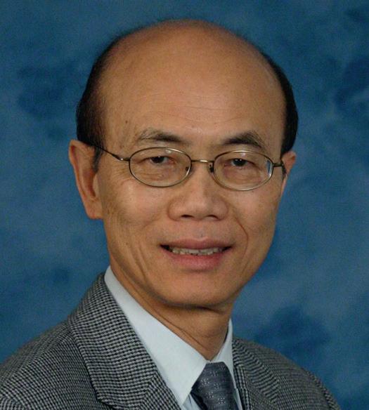
Jin Jang is a Chair Professor at Department of Information Display of Kyung Hee University. His current research programs are in oxide and LTPS TFTs for displays, TFT circuits and TFT application to sensors, Micro-LED, and flexible AMOLED. He invented the first full color AMLCD on plastic substrate, flexible AMOLED, and some new device structures using oxide semiconductors. He is the author or coauthor of over 1000 technical publications of which over 650 are in SCI Journals such as Nature, Advanced Materials, Advanced Functional Materials, IEEE Electron Device Letters and IEEE TED. He is currently a Director of Advanced Display Research Center (ADRC) and had served as Program Chair of SID Symposium 2007 and General Chair of SID Display Week in 2009 and General Chair of IMID 2012, 2013. He is a Fellow of SID and he was awarded George Smith Award from IEEE in 2012, Slotto Owaki Prize from SID in 2015, Jan Rajchman Prize in 2022 from SID, and Ho-Am Award in 2017.

Arokia Nathan is a leading pioneer in the development and application of thin film transistor technologies to flexible electronics, display, and sensor systems. Following his PhD in Electrical Engineering, University of Alberta, Canada, in 1988, he joined LSI Logic USA and subsequently the Institute of Quantum Electronics, ETH Zürich, Switzerland, before joining the Electrical and Computer Engineering Department, University of Waterloo, Canada. In 2006, he joined the London Centre for Nanotechnology, University College London as the Sumitomo Chair of Nanotechnology. He moved to Cambridge University in 2011 as the Chair of Photonic Systems and Displays, and he is currently a Bye-Fellow and Tutor at Darwin College. He has over 600 publications including 6 books, and more than 130 patents and four spin-off companies.
He is a Fellow of IEEE, a Distinguished Lecturer of the IEEE Electron Devices Society and Sensor Council, a Chartered Engineer (UK), Fellow of the Institution of Engineering and Technology (UK), Fellow of the Royal Academy of Engineering, Fellow of the Society for Information Displays, and winner of the 2020 IEEE EDS JJ Ebers Award.
Chapter 22
Dr. Michael F. Tompsett has a first class BA in Physics and a PhD from Cambridge University, UK. He has 18 Patents, authored or coauthored 40 Refereed Papers, many invited talks and conference presentations, a Book and 3 Book Chapters.
A system for monitoring the growth of thin films that he developed in Britain continues to be used today. In 1968, also in Britain, he started the field of uncooled thermal-imaging with the invention of uncooled thermal-imaging camera-tubes, which when used in cameras were immediately adopted by firefighters, because they see through smoke. He also invented a solid-state version, which after extensive development is widely used for night vision, fire-fighting, search-andrescue, and medical applications.
Dr. Tompsett joined Bell Labs in 1969 and is best known for the imaging work described above. He was director of the US Army Electron Devices Research Laboratory from1991 to 1997, before becoming an entrepreneur in 1998 and running his own medical software company until 2012.
He has received multiple awards including the 2010 National Medal for Technology and Innovation, the 2012 IEEE Edison Gold Medal, and in 2017, he shared the Queen Elizabeth Prize for Engineering.
He was also awarded the Royal Photographic Society Progress Medal and an Emmy from the National Academy of Television Arts and Science and was elected a Member of the US National Academy of Engineering.
Chapter 23
Eric R. Fossum, IEEE Life Fellow, is the John H. Krehbiel Sr. Professor for Emerging Technologies with the Thayer School of Engineering at Dartmouth College. He also serves as Director of Dartmouth’s PhD Innovation Program and as Vice Provost for Entrepreneurship and Technology Transfer. He was the primary inventor of the CMOS image sensor with intra-pixel charge transfer, currently used in billions of smartphones and other applications, while working at the NASA Jet Propulsion Laboratory (Caltech) to reduce camera size and power on interplanetary spacecraft. He cofounded and co-led Photobit Corporation to commercialize the technology. At Dartmouth, he developed the CMOS quanta image sensor with his students. The deep sub-electron read noise photon-counting technology was transferred to Gigajot Technology Inc., a successful Dartmouth spinoff he cofounded with his former students. He is a 2017 Queen Elizabeth Prize laureate, a member of the US National Academy of Engineering, and was inducted into the US National Inventors Hall of Fame. He is a Fellow of Optica and the National Academy of Inventors. He was awarded the IEEE Andrew Grove Award, the OSA/IS&T Land Medal, and the NATAS Technical Emmy Award, among other honors. He was the cofounder and the First President of the International Image Sensor Society. To relax, he and his wife enjoy their hobby farm in New Hampshire.
Chapter 24

Henry Baltes (Fellow, IEEE) is Professor Emeritus of ETH Zurich affiliated with Micro and Nano Systems at the Dept. of Mechanical and Process Engineering. He was Professor of Physical Electronics at ETH Zurich and Director of the Physical Electronics Laboratory from 1988 to 2006. He is a member of the Swiss Academy of Technical Sciences and a cofounder of the spin-off company SENSIRION. Among his awards are the Koerber European Science Award, the Wilhelm Exner Medal of the Austrian Trade Association, and the honorary degrees of Doctor of the Universities of Waterloo, Ontario in Canada, Bologna in Italy, Freiburg in Germany, and the University College London in the United Kingdom. He also won the Swiss Technology Award, the IEEE Donald G. Fink Prize Paper Award, and the Robert Bosch Micro and Nano Electro-Mechanical Systems Award. From 1983 to 1988, he held the Henry Marshall Tory Chair in Electrical Engineering at the University of Alberta, Edmonton, Canada. From 1973 to 1983, he worked for a Swiss company and taught at EPF Lausanne. He received the degree of Doctor of Natural Science of ETH Zurich in Physics in 1971.
Chapter 25
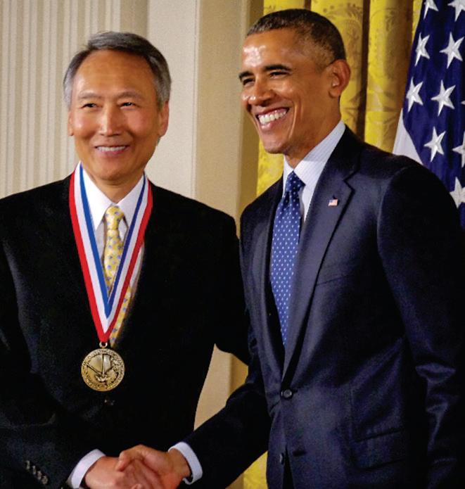
B. Jayant Baliga (F’83-LF’14) received the MS and PhD degrees in electrical engineering from Rensselaer Polytechnic Institute, Troy, NY, in 1971 and 1974, respectively. He spent 15 years at the General Electric R&D Center, Schenectady, NY, leading their power device effort and was bestowed the highest rank of Coolidge Fellow. He joined NC State University in 1988 as a Full Professor and was promoted to Distinguished University Professor in 1997 and subsequently Progress Energy Distinguished University Professor. He founded four start-up companies with successful products while at NCSU.
Dr. Baliga has authored 22 books and over 700 publications in international journals and conference digests. He was honored with the National Medal of Technology and Innovation in 2011 by President Obama at the Whitehouse, the highest IEEE recognition – the Medal of Honor in 2014, the Global Energy Prize in 2015. He holds 122 U.S. patents and was inducted into the National Inventors Hall of Fame as the sole inventor of the IGBT in 2016.