Van der Waals Heterostructures
Fabrications, Properties, and Applications
Edited by Zheng Zhang, Zhuo Kang, Qingliang Liao, and Yue Zhang
Editors
Dr. Zheng Zhang
University of Science & Technology Beijing Department of Materials
Physics & Chemistry
Xueyuan Road 30# Haidian District 100083 Beijing China
Dr. Zhuo Kang
University of Science & Technology Beijing School of Materials Science and Engineering
Xueyuan Road 30# Haidian District 100083 Beijing China
Dr. Qingliang Liao
University of Science & Technology Beijing School of Materials Science and Engineering
Xueyuan Road 30# Haidian District 100083 Beijing China
Dr. Yue Zhang
University of Science & Technology Beijing Department of Materials Physics & Chemistry
Xueyuan Road 30# Haidian District 100083 Beijing China
Cover Design: FORMGEBER Mannheim
Cover Image: (Background) FORMGEBER Mannheim; (Insets) Courtesy of Prof. Zheng Zhang
All books published by WILEY‐VCH are carefully produced. Nevertheless, authors, editors, and publisher do not warrant the information contained in these books, including this book, to be free of errors. Readers are advised to keep in mind that statements, data, illustrations, procedural details or other items may inadvertently be inaccurate.
Library of Congress Card No.: applied for
British Library Cataloguing-in-Publication Data: A catalogue record for this book is available from the British Library.
Bibliographic information published by the Deutsche Nationalbibliothek
The Deutsche Nationalbibliothek lists this publication in the Deutsche Nationalbibliografie; detailed bibliographic data are available on the Internet at http:// dnb.d-nb.de.
© 2023 Wiley‐VCH GmbH, Boschstraße 12, 69469 Weinheim, Germany
All rights reserved (including those of translation into other languages). No part of this book may be reproduced in any form – by photoprinting, microfilm, or any other means –nor transmitted or translated into a machine language without written permission from the publishers. Registered names, trademarks, etc. used in this book, even when not specifically marked as such, are not to be considered unprotected by law.
Print ISBN 978‐3‐527‐34950‐0
ePDF ISBN 978‐3‐527‐83386‐3
ePub ISBN 978‐3‐527‐83387‐0
oBook ISBN 978‐3‐527‐83388‐7
Typesetting Straive, Chennai, India
Contents
Preface xi
1 The 2D Semiconductor Library 1
Zheng Zhang and Yue Zhang
1.1 Introduction 1
1.2 Emerging 2DLMs for Future Electronics 3
1.2.1 Classification 3
1.2.2 Elemental 2DMLs 3
1.2.2.1 IV A Group 3
1.2.2.2 V group A 6
1.2.2.3 III A Group 7
1.2.3 Hexagonal Boron Nitride (h-BN) 8
1.2.4 Transition Metal Dichalcogenides (TMDCs) 9
1.2.5 Transition Metal Carbides (TMCs) 12
1.2.6 Transition Metal Oxides (TMOs) 15
References 18
2 The 2D Semiconductor Synthesis and Performances 33
Xiang Chen, Qijie Liang and Yue Zhang
2.1 Exfoliation 33
2.1.1 Starting from Graphene 33
2.1.2 Semiconducting 2D Materials 34
2.1.3 Big Family of Exfoliated 2D Materials 34
2.1.4 Mechanical Exfoliation of 2D Materials 34
2.1.5 Liquid Exfoliation of 2D Materials 35
2.1.6 Other Exfoliation Method of 2D Materials 37
2.2 Chemical Vapor Deposition 38
2.2.1 Overview of Chemical Vapor Deposition 38
2.2.2 Atmospheric Pressure Chemical Vapor Deposition (APCVD) 40
2.2.2.1 Synthesis of Single-Element Materials (Graphene) 40
2.2.2.2 Synthesis of TMDCs Bielement Materials 42
2.2.2.3 Synthesis of Multielement Materials 48
2.2.3 Low-Pressure Chemical Vapor Deposition (LPCVD) 48
2.2.3.1 Synthesis of Single-Element Materials (Graphene) 48
2.2.3.2 Synthesis of TMDCs Bielement Materials 49
2.2.3.3 Synthesis of Multielement Materials 51
2.2.4 Plasma-Enhanced Chemical Vapor Deposition 53
2.2.4.1 Overview 53
2.2.4.2 Synthesis of Graphene by PECVD 54
2.2.4.3 Synthesis of VG Nanosheets by PECVD 56
2.2.4.4 Synthesis of TMDCs by PECVD 56
2.2.5 MOCVD 57
2.2.5.1 Overview 57
2.2.5.2 Synthesis of III–V Group Semiconductor by MOCVD 59
2.2.5.3 Synthesis of TMDCs by MOCVD 60
References 63
3 The VdW Heterostructure Controllable Fabrications 69 Zheng Zhang, Qingliang Liao and Yue Zhang
3.1 Wet Transfer 69
3.1.1 Substrate Etching Techniques 69
3.1.2 Electrochemical Delamination Methods 72
3.1.3 Wedging Transfer Method 74
3.2 Controllable Selective Synthesis 76
3.2.1 Controllable Synthesis of 2D-2D Heterostructures 76
3.2.1.1 Vertical 2D-2D Heterostructures 76
3.2.1.2 Horizontal 2D-2D Heterostructures 79
3.2.1.3 One-Dimensional Heterostructures 80
3.2.2 Controllable Synthesis of 2D-1D Heterostructures 82
3.2.3 Controllable Synthesis of 2D-3D Heterostructures 85
3.3 Dry Transfer 86
3.3.1 Thermal-release Tape 86
3.3.2 Stamps 88
3.3.3 The Pick-up Methods 89 References 93
4 The Mixed-dimensional VdW Heterostructures 97 Pei Lin, Baishan Liu and Zheng Zhang
4.1 Categorization of Mixed-dimensional VdWHs 97
4.2 Strategies for Constructing Mixed-dimensional VdWHs 99
4.2.1 Transfer-assisted Assembly of Mixed-dimensional VdWHs 99
4.2.2 Direct Growth of Mixed-dimensional VdWHs 100
4.3 Electronic and Sensing Applications 101
4.3.1 Transistors and Spintronics 101
4.3.2 Chemical Sensors 102
4.4 Optoelectronic and Photonic Applications 104
4.4.1 2D-0D Hybridization
4.4.2 2D-1D Hybridization 105
4.4.3 2D-3D Hybridization 108
4.5 Energy Applications 111
4.5.1 Application in Photocatalytic Water Splitting 111
4.5.2 Application in Rechargeable Batteries 112
4.5.3 Application in Supercapacitors 114
4.6 Conclusions 115
References 116
5 The VdW Heterostructure Interface Physics 125 Guangjie Zhang, Yang Ou, Peifeng Li and Qingliang Liao
5.1 Band Alignment and Charge Transfer in VdWHs 126
5.2 Magnetic Coupling in VdWHs 129
5.2.1 Applications in Valleytronics 132
5.2.2 Application in Spintronics 134
5.3 Moiré Pattern 134
5.3.1 Band Structure in Moiré Lattice 134
5.3.2 Flat Band-Introduced Superconductivity in Bilayer Graphene 135
5.3.3 Moiré Excitons 135
5.3.4 Moiré Lattice Topology 136
5.4 VdWHs for Protection 137
5.4.1 Introduction of Hexagonal Boron Nitride 137
5.4.2 Graphene Capsulated by h-BN 138
5.4.3 Transition Metal Dichalcogenides Capsulated by h-BN 140
5.4.4 Black Phosphorus Capsulated by h-BN 141
5.5 Characterization Techniques for VdWHs 142
5.5.1 Scanning Transmission Electron Microscopy for Characterization of Structural and Related Properties 142
5.5.2 Scanning Probe Microscopy for Characterization of Structural and Electrical Properties 144
5.5.3 Optical and Vibrational Spectroscopy for Characterization of Electron-, Exciton-, and Phonon-Related Properties 145 References 147
6 The VdW Heterostructure Multi-field Coupling Effects 157
Junli Du, Baishan Liu and Zheng Zhang
6.1 Introduction 157
6.2 The Multifield Coupling Effect Characterization for 2D Van der Waals Structures 158
6.2.1 The Multifield Microscopy Techniques on 2D VdW Structures 158
6.2.1.1 The Electric-Field-Integrated STM-STS Technique 159
6.2.1.2 The Thermal-Field-Integrated STM-STS Technique 160
6.2.1.3 The Multifield-Integrated TEM Technique 161
6.2.1.4 The Optical-Field-Integrated KPFM Technique 162
6.2.2 The Multifield Optical Spectroscopy Techniques on 2D VdW Structures 163
6.2.2.1 The TERS Technique Based on STM and Raman Spectroscopy 163
6.2.2.2 The S-SNOM Based on AFM 165
6.2.3 The Perspective of Multifield Integration Characterization for 2D VdW Structures 166
6.3 The Multifield Modulation for Electrical Properties of 2D Van der Waals Structures 167
6.3.1 Strain-Engineered Electrical Properties of 2D VdW Structures 167
6.3.2 Electric Field-Engineered Electrical Properties of 2D VdW Structures 169
6.3.3 Thermal-Engineered Electrical Properties of VdW Structures 171
6.4 The Multifield Modulation for Optical Properties of 2D Van der Waals Structures 172
6.4.1 Strain-Engineered Optical Properties of 2D VdW Structures 173
6.4.2 Electric-Engineered Optical Properties of 2D VdW Structures 175
6.4.3 Thermal-Engineered Optical Properties of VdW Structures 177
References 178
7 VdW Heterostructure Electronics 187
Xiankun Zhang, Xiang Chen and Yue Zhang
7.1 Van der Waals PN Junctions 188
7.2 Van der Waals Metal–Semiconductor Junctions 192
7.3 Field-effect Transistor 197
7.3.1 Basic Structure 198
7.3.2 Advantage Characteristics 199
7.3.3 2D Dielectric Materials 199
7.4 Junction Field-Effect Transistor 201
7.4.1 Current–Voltage Features 202
7.4.2 Working Principle 203
7.4.3 Device Structure 205
7.4.4 Applications 205
7.5 Tunneling Field-Effect Transistor 208
7.5.1 The History of TFET 208
7.5.2 Mechanism of TFET 209
7.5.3 Application of TFET 211
7.6 Van der Waals Integration 213
References 216
8 VdW Heterostructure Optoelectronics 223
Qi Zhang, Zhuo Kang and Yue Zhang
8.1 Photodetectors 223
8.1.1 Photovoltaic Effect 228
8.1.2 Photoconductive Effect 229
8.1.3 Tunneling Effect 231
8.1.4 Photo-Thermoelectric Effect 233
8.1.5 Improvement Strategies 234
8.2 Light Emission 236
8.2.1 Light-Emitting Diodes 236
8.2.2 Lasering 242
8.2.3 Single Photon 244
8.3 Optical Modulators 245
8.3.1 All-Optical Modulators 245
8.3.2 Electro-Optic Modulators 246
8.3.3 Thermo-Optic Modulators 247 References 248
9 VdW Heterostructure Electrochemical Applications 261
Xiankun Zhang and Zhuo Kang
9.1 Solar Energy 262
9.2 Van der Waals Heterostructure Application in Hydrogen Energy 267
9.2.1 Producing Hydrogen by Water Photolysis 268
9.2.2 Producing Hydrogen by Water Electrolysis 270
9.3 Battery 271
9.3.1 Lithium-ion Batteries, Sodium-ion Batteries, Potassium-ion Batteries 273
9.3.2 Supercapacitors 276
9.4 Catalyst 277
9.5 Biotechnology 282
9.5.1 Biosensors 283
9.5.2 Tissue Engineering 284 References 286
10 Perspective and Outlook 295
Zheng Zhang and Yue Zhang
10.1 Overall Development Status of 2D Materials 295
10.1.1 Material Preparation: Scalability, Uniformity, and Reproducibility 297
10.1.2 Metrology 297
10.1.3 Construction of Heterostructure: Industry-Compatible Integration Process 299
10.2 Compatibility Between 2D Van der Waals Device Processing and Silicon Technology 301
10.2.1 Compatibility of 2D Van der Waals Device Integration with Traditional Silicon-Based Process 301
10.2.2 Differences Between 2D Van der Waals Devices and Traditional SiliconBased Processes 303
10.2.3 2D Van der Waals Device Integration Beyond Silicon Technology 305
10.3 Promising Roadmap of Van der Waals Heterostructure Devices [Medium term: 5 years, Long term: 5–10 years] 307
10.4 Promising Roadmap of Optoelectronic Device 309
10.5 Conclusion and Prospect 310 References 311
Preface
As the feature size of semiconductor devices keeps shrinking along Moore’s law, the principle that has powered the information technology revolution since the 1960s, the physical limits to silicon‐based transistors have been reached, resulting in severe performance degradations caused by short‐channel effects, gate oxide tunneling, and surge in power consumption. In order to further downscale the transistors without performance degradations in the post‐Moore era, massive research has been carried out to explore revolutionary new materials and devices. Among them, two‐dimensional (2D) layered materials, including graphene, transition metal dichalcogenides (TMDCs), and related van der Waals (vdW) structures, have been proven to possess great potential for future post‐Moore electronics, optoelectronics, etc.
2D materials possess unique properties with covalently bonded in‐plane and dangling‐bond free surfaces, which ensure monolayers can be stacked on top of each other and held together by interlayer vdW forces. Beside, 2D materials can be integrated into a new type of heterostructures with other materials in various dimensions, including zero‐dimensional (0D) nanoparticles, one‐dimensional (1D) nanowires, 2D films, and three‐dimensional (3D) bulk materials, by exceeding the limitation of close lattice match at the interface. Except for 2D‐2D heterostructures, other structures are so‐called mixed‐dimensional vdW heterostructures. In these heterostructures, the weak vdW forces between the neighboring materials make each material maintain its original electronic structure, without the influence of the interface structure variations. The convenience of this combination leads to many new phenomena, devices, and mechanisms, such as the 0D‐2D photo gating effect, static electrical doping, and 1D‐2D nanowire gating. The underlying physics phenomena and possible applications in integrated circuits, sensors, or energy harvesting have attracted broad interest in academia and industry. In a word, vdW heterostructures provide the promising opportunity to combine different materials with unique properties as the building blocks of engineering new functional structures for the fabrication and applications of 2D electronic and optoelectronic devices.
Our group has been devoted into TMDCs semiconductors and their 0D‐2D, 1D‐2D, 2D‐2D, and 2D‐3D vdW heterostructures since 2013. Recently, along with the highly developed multi‐disciplinary integration, considerable progress has been achieved in fundamental research and technological applications of TMDCs vdW
heterostructures. This book covers state‐of‐the‐art theoretical and experimental research on vdW heterostructures and their applications as electronic and optoelectronic devices. This book is divided into 10 chapters and guided by Dr. Zheng Zhang, Dr. Yue Zhang, Dr. Zhuo Kang, and Dr. Qingliang Liao. The detailed chapter theme and authors are as follows: Chapter 1, “The 2D semiconductor library” (Zheng Zhang and Yue Zhang); Chapter 2, “The 2D semiconductor synthesis and performances” (Xiang Chen, Qijie Liang, and Yue Zhang); Chapter 3, “The vdW heterostructure controllable fabrications” (Zheng Zhang, Qingliang Liao, and Yue Zhang); Chapter 4, “The mixed‐dimensional vdW heterostructures” (Pei Lin, Baishan Liu, and Zheng Zhang); Chapter 5, “The vdW heterostructure interface physics” (Guangjie Zhang, Yang Ou, Peifeng Li and Qingliang Liao); Chapter 6, “The vdW heterostructure multi‐field coupling effects” (Junli Du, Baishan Liu, and Zheng Zhang); Chapter 7, “VdW heterostructure electronics” (Xiankun Zhang, Xiang Chen, and Yue Zhang); Chapter 8, “VdW heterostructure optoelectronics” (Qi Zhang, Zhuo Kang, and Yue Zhang); Chapter 9, “VdW heterostructure electrochemical applications” (Xiankun Zhang and Zhuo Kang); Chapter 10, “Perspective and outlook” (Zheng Zhang and Yue Zhang). In addition to the help of the aforementioned members, the completion of the book is also inseparable from the unremitting efforts of the following doctoral students, including Huihui Yu, Li Gao, Wenhui Tang, Xiaofu Wei, Mengyu Hong, Ruishan Li, Yihe Liu, He Jiang, Kuanglei Chen, Haoran Zeng, Yanzhe Zhang, and Xuan Yu. With this book, I wish to thank my current and former group members, as well as the outstanding colleagues and collaborators who have dedicated themselves to this crucial research area.
The University of Science and Technology Beijing and the funding agencies also have my appreciation for providing the necessary support of the research work. Among the latter, special thanks are due to the National Natural Science Foundation of China (Nos. 51991340, 51991342, 92163205, 51972022), the National Key R&D Program of China (No. 2018YFA0703503), the Overseas Expertise Introduction Projects for Discipline Innovation (No. B14003), and the Natural Science Foundation of Beijing Municipality (Grant No. Z180011).
I worked consistently to accomplish this work with Wiley publisher. I hope that this contribution would further enhance the applied material sciences, especially in bringing new entrants into the nanotechnology fields, and help scientists to come forward and develop their own field of specialization.
Last, but by no means least, I am deeply appreciative of the understanding and support shown by my family members, without whom these achievements could never be obtained.
Dr. Yue Zhang
Academician of Chinese Academy of Sciences Fellow of Royal Society Chemistry
Editor‐in‐chief of National Science Open Engineering and Materials Science Associate Editor of Fundamental Research E‐mail: yuezhang@ustb.edu.cn
1.2 Emerging 2DLMs for Future Electronics
The rise of graphene with excellent properties has facilitated the discovery and research of new two-dimensional materials. In addition to graphene, various twodimensional materials are attracting focus because of their unique properties. The size effect and adjustability of its energy band structure result in some novel properties. In this section, we will look at two aspects of the emerging 2DLMs. In one part, we will give clues based on the structure of two-dimensional materials, and in the other part, we will detail the various 2DLMs that are classified by their elemental composition.
1.2.1 Classification
Initially, 2DLMs represented by graphene were referred to as a layered material that has strong intralayer covalent bonds and weak interlayer vdW coupling. Therefore, the layered material can be obtained by stripping the bulk material. In this case, we call them two-dimensional layered materials (2DLMs).
Lamellar vdW materials, which are separated into single or several layers, are one of the hot research topics. Due to the strong covalent bonds in planes and weak interlayer vdW coupling, they can be separated by mechanical or liquid stripping to form nanosheets [8, 25]. In addition to graphene, which was first discovered, transition metal dichalcogenide (TMDCs) are also typical vdW materials, such as MoS2, WS2, and WSe2. To date, more than 40 types of TMDCs have been discovered [26]. Hexagonal boron nitride (h-BN) [27], silicon carbide [28], VO2 [29], and telluride antimony [30] are also included within such category.
1.2.2 Elemental
2DMLs
2DMLs such as III-VA group and transition group are of great interest. Because of their unique ultrathin two-dimensional limit, they exhibit superior electronic, photonic, magnetic, and catalytic properties than bulk materials. These materials are of great potential for diverse applications in field effect transistors (FET), optoelectronics, memories, and artificial synapsis [31].
1.2.2.1 IV
A Group
Since its discovery in 2004, graphene with the feature of honeycomb structure has been attracting great attention [2]. A range of methods for preparing graphene, such as mechanical stripping, liquid-assisted stripping, and chemical vapor deposition (CVD) methods, have rushed out. It has lots of superior properties, in particular its unprecedented high intrinsic mobility of 200 000 cm 2 V−1 s−1 at room temperature [32]. Stampfer et al. discovered that it has the mobility at low temperature of 350 000 cm2 V−1 s−1, as shown in Figure 1.2a, reaching the highest record so far [35]. The grooves are utilized to suspend graphene. The beam of laser is concentrated on graphene, after which the heat flows radially from the graphene center to the peripheral. The dependence of Raman G peak on excitation power is measured, and

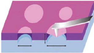

Figure 1.2 Brief introduction of graphene. (a) Relationship between conductance and density of charge carrier. The black and blue plots were obtained at 300 and 1.6 K, respectively. The green one is consistent with carrier mobility μ = 350 000 cm2 V−1 s−1 from another sample. Source: Reproduced with permission from Ref. [33], © American Chemical Society 2008; (b) schematic of configuration about suspended graphene being indentated. (c) Elastic stiffness statistics histogram of graphene. Source: Figure (b) and (c) reproduced with permission from Ref. [34], © Wiley Online Library 2010.
the TC of graphene is approximately 5000 W m−1 K−1 [33]. Graphene was suspended, and Young’s modulus was characterized by patterning a circular well array having a 1.5 mm diameter and 500 nm depth on a SiO2/Si substrate (Figure 1.2b). Figure 1.2c shows the elastic stiffness statistical histogram of suspended graphene. Young’s modulus obtained by this method is about 1.0 T Pa [36]. Therefore, graphene has shown great prospect in applications of electronics, optoelectronics, energy storage, and conversion.
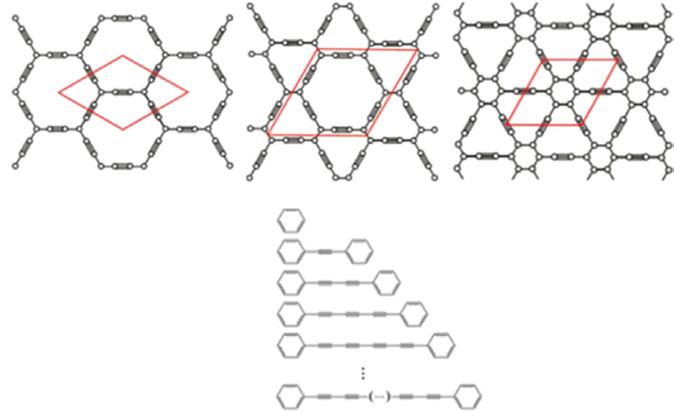
However, graphene still faces significant challenges because of its zero-bandgap nature, which hinders its eventual application. Another two-dimensional allotrope of carbon breaks the ice. The graphite acetylene and its derivatives composed of spand sp2- hybrid carbon atoms have a certain bandgap in the band structure [37–39]. In graphene-acetylene and its derivatives, the alkyne bond is a structural unit that can be inserted to modify the graphene and retain the symmetry of the hexagon.
Figure 1.3a shows the transformation of graphene to α-, β-, and γ-graphene by
Graphdiyne
Graphtriyne
Graphtetrayne
Graph-n-yne
Figure 1.3 Structure and optoelectronic applications of graphite–acetylene group materials. (a) Structure of alpha-, beta-, and gama-graphene. Source: Figure (a) reproduced with permission from Ref. [39], © American Chemical Society 2011; (b) expansional diagram of n-alkyne based on chain length. Source: Reproduced with permission from Ref. [40]/ © American Chemical Society 2013.
inserting acetylene bonds between two carbon atoms in different ways [38]. The structure shown in Figure 1.3b is formed by graphite diacetylene when two acetylene bonds are inserted [39]. Acetylene chains of different lengths will generate a series of graphitic alkynes, such as graphitic alkynes, graphitic dialkynes, graphitic trialkynes, and graphitic tetrapyne. [41]
As one of the graphyne derivatives, graphdiyne can be grown by cross-coupling with hexaethynylbenzene as precursors [40, 42–45]. In general, graphdiyne can be obtained as nanowalls (NWs) [44, 45], film [42, 43], or coating layers covering TiO2 [40] by this coupling reaction. In recent years, graphdiyne was successfully prepared on the Au (111) crystal plane using molecular evaporator deposition of precursor molecules in the ultrahigh vacuum ambient of an scanning tunnelling microscopy (STM) [46]. Nishihara et al. successfully prepared multiple layers and few layers of graphite-diacetylene through liquid/liquid or gas/liquid interface reactions [47]. Its properties are predicted successfully by theoretical calculation. Graphyne allotropes feature an intrinsic bandgap (~ 1.2 eV for graphyne and ~ 0.46 eV for graphdiyne), and their direct bandgaps indicate their potential applications in optoelectronic devices [48, 49]. Two-dimensional graphene with Dirac dots and cones still exist, such as α-graphene with a single Dirac cone and 6,6, 12-graphene with two different Dirac cones [49, 50]. The different atomic structure of graphyne alkyne results in the difference of electronic structure [51]. Graphyne group material as a new 2DLM has excellent application prospects in electronic devices and photovoltaic devices [40, 43, 49]. Li et al. constructed a solar cell with
Graphyne
high efficiency electron transport based on graphite-diacetylene doped benzeneC61-methyl butyrate, as shown in Figure 1.3 [52]. Although graphyne family materials have excellent carrier mobility with a proper bandgap, the challenge of synthesizing single crystal with large scale and high quality has severely limited the further application development of graphite-based alkyne. Wherefore, new methods are urgently needed to achieve the preparation of such high-quality materials.
In addition to carbon, other elements of the IVA group can also form 2DLMs, including silene, germanene, and tinene. The atoms in silicene or germanene are connected with each other through sp3 hybridization, which is more stable than the sp2 hybridization. Even if they are not able to exist as independent lamellae, they can still be successfully obtained as layered materials. At present, lots of methods have been reported to grow silene. One of the most effective methods of wet chemistry is the stripping of 2DLMs by an exchangeable Ca layer and an interlinked Si6 ring consisting of CaSi2 [53]. Some used HCl solution and Mg to further reduce layer-to-layer interactions [54, 55]. In addition, the most common approach is the vapor deposition on selected substrates, such as Ag (111) [56], Ag (110) [57], Au (110) [58], Ir (111) [59], MoS2 [60], ZrB2 [61], and H-MoSi2 [62] in STM. Excellent physical features of silicene, including the quantum spin Hall effect [63, 64], ferromagnetism [65, 66], germanium doping controlled TC [67], and semi-metallic properties [68] have been predicted by theoretical calculations [69].
Germanene can be prepared in a comparable method as silicene, including CaGe2assisted chemical exfoliation [70] and vapor deposition [71–73]. Germanene features a number of exclusive characteristics, including robust structure [74], semimetallic property [75], high exciton resonance [76, 77], high carrier mobility [78], Dirac characteristics [79, 80], photon properties of ground state [81, 82], negative thermal expansion [83], spin electron transport [84], tunable magnetism [85], many body effects [86], infrared absorption [87, 88], and great thermoelectric properties [89]. The charge carriers of germanium materials, whose electronic structure is similar to graphene and silicon, are massless fermions. Using a vertical electric field can open the bandgap in a single layer of flexed silicon and germanene [90]. In addition, novel properties of the quantum spin hall effect are able to be realized by halogen or hydrogen elements modification [91, 92].
The Sn (111) diatomic layer where two triangular sublattices are stacked to generate a crooked honeycomb lattice that forms the stanene. Based on the substrate Bi2Te3 (111), stanene can be prepared by molecular beam epitaxy (MBE) [93]. Excellent properties have been predicted through theoretical calculations [94], such as stress-affected mechanical properties, novel thermal transport diffusion properties [95, 96], unique electronic features [97], phase transition between topological phase to insulating one [98], large magneto-resistive [99], super conductivity [100], and quantum spin Hall effect [101].
1.2.2.2 V group
A
Two-dimensional materials composed of V-A group elements include black phosphorus (BP), arsenic, antimony, and bismuth. In 1914, BP was successfully prepared [102, 103], where each atom was covalently connected to three adjacent atoms
to create a folded monolayer honeycomb. [104] From bulk to monolayer, the bandgap of BP increases (0.3 up to 1.5 eV). In addition, it has been proved that the room temperature carrier mobility of BP in several layers of quasi-2D phosphors is up to 1000 cm 2 V−1s−1 [105]. Therefore, BP shows significant prospect in applications of electronic and photonic devices [106]. Current methods for producing BP include mechanical stripping [107–109], liquid stripping, [110–113] and CVD [114]. At the same time, the thickness of BP determines its properties, for example photoluminescence (PL) spectroscopy [109, 110]. BP has been demonstrated to show great potential applications in photoelectric fields [107], including photodetectors and solar cells. [115] BP is studied through simulation experiment and theory analysis of many properties, including stacking-sequence-dependent electronic structure [116–118], anisotropic properties [114], transmission characteristics between magneto-optical [119], controlled band structure [120, 121], flexibility [122], thermal properties [123], anisotropic exciton [124], and electrical conductance [125]. Interestingly, blue phase [126, 127] and topological insulator conversion of BP are proved [128].
Structurally, a layer of arsenic atoms with a rhombic structure forms arsenic. Thickness of 14 nm arsenic was successfully grown on InAs substrate via plasmaassisted process [129]. It has been theoretically calculated that arsenic has many exclusive characteristics, covering anisotropic-controlled TC [130] and strainmodulated topological insulator conversion [131].
The most stable V-A group allotropes is antimonene with monolayer antimony. The bandgap is predicted as 2.28 eV. At present, the approaches of preparing antimonene are mainly mechanical stripping [132], liquid exfoliation [133], MBE [134], and CVD [135]. Antimonene is predicted theoretically to feature some novel characteristics, including spin–orbit coupling (SOC) effect [136], geometry-controlled TC [137], defects-controlled electronic properties [138], and UV detection [139]. Indirect to direct bandgap transition would occur through a small stress, further advancing its potential in optoelectronic applications [140, 141].
In 2005, bismuth was first grown on atomically smooth surfaces [142]. After that, bismuth was successfully obtained by wet chemical synthesis [143]. Theoretical calculations show that bismuthene has a lot of nice attributes. At high temperature, bismuth is insensitive to long wavelength vibration and thermal excitation. As the 3D bulk is scaled into individual single-layer sheets, the bismuthene’s structure is compressed, resulting in a transformation from a semi-metal to a semiconductor. Nevertheless, such thickness dependence does not affect the topological characteristics of bismuthene [144, 145].
1.2.2.3 III A Group
In Group III A, the last specific elemental 2DM is borophene. Boustani first proposed the quasi-planar boron structures through theoretical calculations [146]. Later, methods for preparing borophene, such as vapor deposition [147, 148] and two-growth-zone CVD, were reported [149]. More simulations show that borophene has lots of special attributes, such as high work function [150], magnetism [151], and extremely high hydrogen storage capacity [152]. In addition, two-dimensional
borophene has potential applications of power generation, electrical transmission, energy storage, and electrocatalysis [153, 154].
1.2.3 Hexagonal Boron Nitride (h-BN)
After the discovery of graphene, atomically thin h-BN has also attracted continuous attention in the field due to excellent performance and potential application prospects. The single-layer h-BN has a crystal structure similar to graphene, so it is often referred to as “white graphene.” It consists of alternating covalent B and N atoms in a hexagonal basal plane (space group = P63/mmc) and is free of dangling bonds between the layers (Figure 1.4a,b). These layers stack together to form the bulk crystal by the vdW force [159]. The bulk h-BN shows lattice constants (a = 2.504 Å) and interlayer distances (3.30−3.33 Å) [155].
Having different physical properties from graphene, h-BN is a typical insulator with high relative permittivity and an indirect bandgap of about 6 eV. In addition, h-BN has many other properties including chemical stability, thermal stability, high TC, great mechanical flexibility, atomically flat surface, free of dangling bonds, and charged impurities [156]. This makes h-BN in the field of microelectronics, especially in the vdW electronic field, a broad application prospect. First, h-BN is an appealing substrate dielectric for 2D material-based devices [160]. Compared with traditional substrate dielectric, graphene and other two-dimensional materials using h-BN as dielectric substrate can improve the carrier mobility and realize rapid


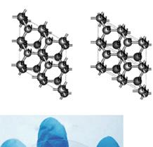
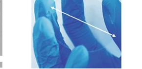
Figure 1.4 (a) Crystal structures of h-BN. Source: Reproduced with permission from Ref. [155], © Chemical Reviews 2017; (b) three structures of h-BN all have space group P63/ mmc and can be transformed into one another by translational gliding moves of the BN plane. Source: Reproduced with permission from Ref. [155], © Physical Review B 2003; (c) exfoliated h-BN nanosheets from h-BN single crystals on the 90 nm SiO2 substrate. Source: Reproduced with permission from Ref. [156], © Nano Micro small 2011; (d) photograph of a wafer-scale SC-hBN film on a SiO2-Si wafer. Source: Reproduced with permission from Ref. [157, 158], © Advanced Materials Interfaces 2018.
heat dissipation at the same time. This can significantly improve the device performance while maintaining the intrinsic performance of the channel material. Second, the high stability and two-dimensional honeycomb structure of h-BN can be applied in device packaging [161]. The dense six-membered ring structure of h-BN can isolate the influence of external atoms on internal devices, protecting the TMDCs channel material from the corrosion of water and oxygen in the air. Furthermore, the tunable tunneling barrier of h-BN has potential applications in tunneling, optoelectronic, and memory devices [162]. Recently, it has been found that h-BN, as a natural hyperbolic and piezoelectric material, exhibits some new optical and electromechanical properties [163]. These unique properties also make it a candidate for practical applications of hyper lenses, near-field imaging, deep ultraviolet emitters and detectors, quantum optoelectronics, and nonlinear and stretchable optical devices [164].
Obtaining large-size and high-quality h-BN film is the primary problem for realizing its application. Up to now, h-BN is usually prepared by mechanical exfoliation and CVD. The mechanical exfoliation can achieve high-quality and few-defect h-BN flakes (Figure 1.4c), but due to the small size and limitation of yield, it is usually used for proof-of-concept of a single prototype device. CVD is considered to be an ideal solution for low-cost, high-reproducibility, and large-scale preparation of h-BN. The current breakthrough in CVD growth of h-BN is the successful preparation of wafer-scale single-crystal film (Figure 1.4d) [157]. Besides, other 2D materials can be epitaxially grown directly onto h-BN by CVD method to form high-quality heterostructures with clean interface and controllable stacking sequence [165].
1.2.4 Transition Metal Dichalcogenides (TMDCs)
Two-dimensional TMDCs are a class of promising materials with attractive properties in the basic research of new physical phenomena and applications in fields ranging from electronics and photonics to sensing and actuation. The generalized formula of TMDCs is MX2 where M and X are transition metal element and chalcogen element (S, Se, or Te), respectively. MoS2 monolayers have demonstrated the applications of transistor [11] and PL since 2010. After that, TMDCs are regarded as highly promising candidates for next-generation electronics and photonics [166, 167].
Recently, the vdW integration primarily stimulated 2D device research. The highquality vdW heterostructures with low production cost and short development processes are reported and applied in the field of physics and electronics [168, 169].
Most TMDCs are dangling bonds free and thus exhibit high mobility. Meanwhile, the selection of suitable substrate, metal contact, and mobility restrain caused by grain boundaries are also crucial for electronic device [170]. For example, mobility of MoS2 on SiO2/Si substrate with BN/Si substrate (encapsulated) and scandium contact is 33–151 cm2 V−1 s−1 and 700 cm2 V−1 s−1 at room temperature, respectively [171, 172].
The structure of TMDCs was first reported in 1923 by Linus Pauling. After that, around 60 TMDCs were found in the late 1960s [173]. The ultrathin MoS2 layers are obtained by tape exfoliation by Robert Frindt in 1963 [174]. Monolayer MoS2
suspensions were produced in 1986 [175]. Since 2004, the rapid development of graphene-related research has led to the development of technologies for layered materials, opening a new way for research on TMD, especially for ultrathin films [176].
Here we will introduce the structure and electronic band structure of TMDCs. The typical atomic ratio of TMDCs (MX2) is one transition metal atom (Ti, V, Ni, Zr, Nb, Pd, Hf, Ta, Ir, Pt, Mo, and W) stuck in two chalcogen atoms (S, Se, and Te), while some other cases are 2 : 3 (M2X3) with quintuple layers, or 1 : 1 (MX) [177–179].
Stacking sequence affects the electronic band structure, phonon vibration, optical properties, and other outstanding physical properties of the material [180]. There are two common structural phases of TMDCs that are 2H and 1T. The H and T are the acronyms of hexagonal phase with trigonal prismatic structure and tetrahedral phase with octahedron structure, respectively. The stack sequence of TMDCs is indicated in the numbers of phase name such as “2” H, “1” T, “3” R, and “4” H. For example, 2H-MoS2 possesses a two-layer AB stacking, and 3R-NbS2 possesses a repeating three-layer ABC stacking. The H-phase material belongs to hexagonal symmetry, and each metal atom extends six branches out to two tetrahedrons in z and +z directions. The chalcogen-metal-chalcogen arranged along z direction are considered to be monolayer, and the vdW interaction between each layer (chalcogen–chalcogen) is weak, which makes the bulk TMD mechanically easy to peel into a monolayer flake [178]. The T-phase structure TMDCs consists of a trigonal chalcogen layer on the top and a 180-degree rotation structure at the bottom. The stacking configuration of the individual layers in multilayer and bulk samples and possible distortions further describe the structure of TMDCs [181, 182]. These pronounced distortions can lead to the formation of metal–metal bonds, which result in the 1T′ phase in the dimerization of the 1T phase of group VI TMDCs. The charge density wave phase is also associated with the weak lattice distortion that shows rich physics and complex phase diagrams.
Except for WTe2, the 2H phase and 1T phase common bulk phase TMDCs formed by VI transition metals (Mo or W) and chalcogen (S, Se, or Te) are thermodynamically stable and metastable, respectively. Orthorhombic 1T′ phase WTe2 is the stable bulk phase that is different from other TMDCs. The cohesive energy difference between 1T′ phase and 2H phase MoTe2 is beneficial to the modulation between them. In addition, the dichalcogenides of the transition metals such as Ti, Cr, Ni, Zn, V, Nb, and Ta just exhibit simple metal behavior [6]. 2H structure involves the hexagonal group (group name: P63/ MMC); the hexagonal lattice consists of two alternating sulfur atoms and a transition metal atom. Although most of 2H structures exhibit semiconductor properties in layer TMDCs, very few 2H phases exhibit metal behavior, such as 2H-NbS2, 2H-NbSe2, 2H-TaS2, and 2H-TaSe2 [183, 184].
The primary structure of metallic-layered TMD is 1T phase that belongs to the hexagonal basis. Due to the rotation of one tetrahedron, the resulting structure is an octahedron.
The dimerization of the transition metal atoms causes the distortion of the 1T structure to form the 1T’ phase, especially the displacement in an out-of-plane direction and a symmetry transformation of chalcogen atoms. The difference
between 1T and TD is C-axis angle (α 90, β = 90). The 3R phase consists of three layers in one unit cell. For example, NbS2, NbSe2, TaS2, and TaSe2 appear in the H and T phases, as well as in the 3R phases [186].
Due to the diversity of its chemical composition and structural phases, TMD has a wide range of electrical properties, such as band structure characteristics (metal or insulation) and the appearance of correlated and topological phases.
The bulk phases of TMDCs are indirect bandgap.
Most of the semiconductor-layered TMDCs such as MoS2 (1.8 eV), MoSe2 (1.5 eV), (2H)-MoTe2 (1.1 eV), WS2 (2.1 eV), and WSe2 (1.7 eV) exhibit direct bandgap in monolayer, whereas their bulk phases are indirect bandgap except a few cases such as GaSe and ReS2 [187, 188]. The formation of TMDCs by the combination of Mo, W, S, and Se with VI group transition metals is discussed. MoS2, WS2, and WSe2 display semiconducting properties in their thermodynamically stable 2H phase that drew attention to the application for electronic devices [11].
According to the first principle (density functional theory), the band structure of 2H-MoS2 evolved from the bulk to monolayer is shown in Figure 1.5. With the thickness of 2H-MoS2 decreasing, the upshift of valence band edge and the downshift of conduction band edge changes, and the indirect bandgap semiconductor block material is transformed into direct bandgap semiconductor monolayer material. The bulk and monolayer 2H-MoS2 display bandgap values of 0.88 and 1.71 eV, respectively. The experimental bandgap of 2H-MoS2 monolayer is 2.16 eV [189].


Figure 1.5 (a) 2H, 1T, 1T′ structures schematic diagram of layer TMDCs. Source: [180], © Materials Today 2017; (b) the band structure of 2H-MoS2 changes from bulk to monolayer. Source: [166], © Nano letters 2010; (c) schematic illustration of the electronic band structure of monolayer TMD materials. Source: [185], © Physical Review B; (d) various physical properties such as magnetism (ferromagnetic is abbreviated to F in the table and antiferromagnetic is abbreviated to AF in the table), superconductivity (S in the table), charge density wave (CDW in the table), and corresponding crystal structures (2H, 1T) of various 2D TMD and other 2D materials. Source: [180], © Materials Today 2017.
Importantly, the maximum value of the valence band and the minimum value of the conduction band are located at two unequal points of high symmetry, K and K′ , which correspond to the corners of the hexagonal Brillouin zone. Monolayer 2H-MoS2 along with other group VI monolayers 2H-TMDCs and graphene have this property commonly and could realize the observation of valley-related physical phenomena and potential valley electronics applications.
1.2.5 Transition Metal Carbides (TMCs)
Transition metal carbides (TMCs) have a high conductivity, good hydrophilicity, and various surface terminations that are applied in the fields of electrogenerated chemiluminescence, catalysts, biosensors, anti-pollution and anti-bacterial agents, and biological detection [190–192]. Their good stability at high temperature also shows adequate reproducibility. Therefore, there is a high demand for TMCs, such as two-dimensional (2D) form (MXene), nanocomposites, nanoparticles, carbide films, carbide nanopowders, and carbide nanofibers. [193, 194]
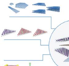
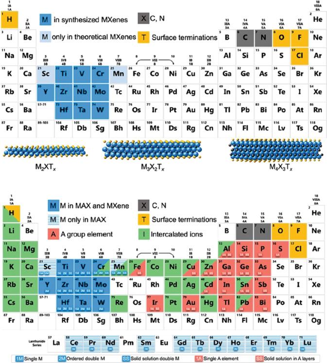
MXene was first reported in 2011, after that, 70 different MXenes such as Ti2CTx, Ti3C2Tx, and Nb4C3Tx have been synthesized, most of which belong to the 2D class of carbides [195]. Considering that over 100 stoichiometric structures have been predicted and can produce an infinite number of solid solutions, MXene is likely to be the largest 2D material family known to date.
Mn+1XnTx is the general formula of MXenes (M = early transition metal, X = carbon/nitrogen, n = 1, 2, 3, 4, Tx = surface terminations such as -OH, -F, -O) (Figure 1.6). MAX is the precursor of Mxenes where A is element of IIIA or IVA. By the etching “A” layer from MAX (the precursor of MXene, having the general formula Mn+1AXn, A = aluminum) the MXenes are formed. The elements to form MAX phases, MXenes, and intercalated ions are shown in Figure 1.6. [197]
Most MXenes are carbides containing only one metallic element such as Ti3C2, Ti4C3, VC2, and V4C3 [198]. Besides, binary metal carbides are also reported and two kinds of metals are located on the surface and in the middle of the MXenes, respectively (Mo2TiC2 or Mo2Ti2C3) [199, 200]. Predictable compositions of Mxenes are greatly increased due to the abundant surface teminals, such as -O, -OH, -F, -Cl, -Br, and -S. Futhermore, the physical and chemical properties can be tuned by the surface terminals [196, 201]. For example, Wu has synthesized 2D MoS2/Ti3C2 composite with surface terminations to provide edge-active sites for hydrogen evolution reaction (HER). The oxygen termination and hydronium ions bond/debond with each other in the acid media properly to effect the oxidation process during the charging and discharging process that improves the pseudo-capacitance.
Ordered phases and solid solutions are two different forms of MXenes. The transition metals are arranged randomly in solid solutions, while one transition metal layer lies between the layers of another transition metal in the ordered phase [193].
Except for the pure metal and carbon phases, the phases formed in the TMC system can be categorized as Hägg carbides (interstitial carbides). In Hägg carbides, a tightly stacked sequence was formed by metal atoms and the carbon atoms in Mxenes occupy the most (octahedral) interstices. All phases often appear to contain
(b)
Figure 1.6 Compositions of MXenes and MAX phases in periodic tables. (a) Elements contained in MXenes. The bright blue elements represent MXenes that have not been yet experimentally confirmed. Schematic diagrams of three typical MXene structures are shown at the bottom; (b) elements used to build MAX phases, MXenes, and their intercalated ions. Elements with blue striped background have only been reported in Mxenene precursors (MAXC phase), and their Mxenes have not yet been synthesized. The element on the red background is element A in the MAX phase, which can be selectively etched into Mxenes. The green background shows the cations that have been intercalated into MXenes to date. According to the legend below, 1M and 1A represent the formation possibilities of a single (pure) transition metal and An element Max phase (and Mxene)1M and 1A indicate the formation possibility of a single (pure) transition metal and An element MAX phase (and MXene). SS indicates the existence of solid solutions in transition metal atomic planes (blue) or element planes (red); 2M indicates the possibility of the formation of ordered double transition metal Max phase or MXene (either in-plane or out-of-plane). Source: [196]. © ACS nano 2019.
(a)
a large number of nonstoichiometric components that are classified as strongly nonstoichiometric compounds [202].
Face-centered cubic (FCC) sublattice is always formed by metal atoms in the group IVB carbides. While on the other hand, the FCC sublattices are maintained only to the extent that the homogeneity of transition metals and carbon is approximately equal. When the ratio of metal:carbon approaches 2 : 1, which is M2C, a hexagonal, tightly packed sublattice was formed by metal atoms. Between these two components, the VB group of carbides may form a mixture of FCC and hexagonal close-packed sequences of metal atoms, which are often indicated as the Zeta (f) phase.
Carbon sublattices offer the possibility of another set of phases, which is also very significant.
It is equally important to consider the carbon sublattice, which provides another interesting set of phase possibilities. The metal sublattice, chemical composition, and the temperature are factors that control the nonmetal sublattice.
In the case of equal amounts of metal and carbon, the B1(rock salt) structure is formed by filling all the octahedral gaps of the FCC metal sublattice with the carbon atoms.
Whereas, in substoichiometry, the actual chemical content and temperature affect the order arrangement of carbon atoms filling the octahedral gap.
Therefore, deviations from local stoichiometry tend to change the structure of carbon sublattices, whereas metal sublattices changing requires a dramatic change in stoichiometry.
Carbon sublattices act as solid solutions between carbon atoms, and structural vacancies should also be considered. This is important because the interaction between chemistry and structure is emphasized; furthermore, the potential of carbon sublattices to arrange themselves in an orderly manner at lower temperatures is also mentioned. Here, we briefly introduce the different structures of MX, M6C5, M4C3, M3C2, and M2C.
MX crystal structure have a stoichiometry of 1:1. The metal atoms occupy an FCC lattice, while all the octahedral interstitials are occupied by the carbon atoms. This rock salt (B1) phase exists in the carbide of IVB and VB groups, and they are stable in the temperature range from room temperature to the melting point.
When the carbon in B1 structure is slightly lost, vacancy-ordered structures such as the M6C5 composition could be predicted. The V8C7 structure has also been reported in some cases. As the number of carbon lost is more, there are two kinds of structure near the ideal compositions of M4C3 or M3C2: (i) B1 structure with vacancy-ordered forms and (ii) phases with mixed FCC/hexagonal close-packed metal atom stacking sequences (also called stacking fault phases). Stable M2C crystal structures has been achieved with the carbon depletion sufficiently, either as a vacancy-ordered form of the B1 structure that is normally present in the group IVB carbides or as a structure based on a hexagonal close-packed arrangement of the metal atoms with the carbon atoms occupying the octahedral interstices as observed in the group VB carbides. As been reported, for the vacancy-ordered forms of the B1 structure, the vacancies on the M2C component can be arranged in a variety of ways [203].
1.2.6 Transition Metal Oxides (TMOs)
In comparison with other atomic thin materials, transition metal oxides (TMOs) have a relatively long usage history. They contain many of the earth’s rich minerals and have been used for thousands of years as building materials, thermal treatment, pigments, lubricants, and many other applications. TMOs are composed of transition metals in the D region of the periodic table and oxygen. TMOs have the ability to change their bond structure and thus change their oxidation state, depending on the particularity of their chemical composition and crystal structure and are relatively easy to cause oxygen defects. Two-dimensional (2D) TMOs usually exhibit different physical and chemical properties compared to their bulk bodies. These differences increase the excellent properties, including the electronic properties of high-temperature superconductivity and multiferroicity, as well as the unique optical, mechanical, and thermal phenomena. Besides, the catalytic and chemical properties of TMOs can be changed by reducing their thickness. These properties result in potential applications that have been realized in the fields of optics, electronics, catalysis, energy components, sensors, and biological systems. Other emerging applications have been proven in piezoelectric, thermal elements, and superconductors [8, 204–206].
The unique characteristics of oxygen ions is the critical factor to produce excellent performance on the surface of TMOs, and especially for 2D TMOs, this surface performance dominates the performance of the material [207]. O2− ions have strong polarization. This polarization allows the planar TMO to exhibit a large, nonlinear, and uneven charge distribution within its crystal lattice, resulting in electrostatic shielding on the length scale of 1–100 nm, resulting in an excellent local surface and interface features. Therefore, the specific energy state exists near or on the surface of planar TMOs, which are quite different from their bulk state, and also causes strong Coulomb interactions between the 2D TMOs and adjacent ions [208]. If surfaces of two TMOs are close to each other, a built-in interface potential can be generated, changing the Fermi level of the surface plane that will significantly affect its electronic properties. In this type of planar TMOs, different atomic orbitals may contribute to the electronic states. The surface of TMOs can also be activated by electrons due to the hybridization of ion orbitals. If the D orbits of 2D TMO are perpendicular to their plane arrangement, the orbital order and spin order may be frustrated or generated [205, 207]. This creates unconventional semiconductor characteristics.
There are many kinds of transition metals that can be used to form TMOs. Many basic properties of TMOs depend on the types of cations and their flexibility to change the oxidation state. Especially in 2D TMOs, a large number of structures can only be stabilized by cations with different charge states and binding configurations [209]. For the same TMO layer under different stoichiometric ratios, the various electronic properties of metal to wide gap insulation behavior are caused by different metal oxidation states. The metal-insulator phase transition as a function of pressure and temperature is caused by the local properties of the d electronic state. 2D TMOs have a variety of bandgaps, providing the possibility to adjust optical
and electrical properties at almost any wavelength [205]. Nanostructured TMOs have unique redox characteristics, many of which show a reversible trend. Excellent chemical and thermal stability is also possessed by many 2D TMOs [210]. The oxygen vacancies in nanostructured TMO can be changed by various mature procedures to achieve significant tunability [211]. Furthermore, the surface chemistry and bulk structure of 2D TMOs are significantly different due to the decrease of oxygen vacancy formation energy and the increase of reducibility of metal cations [212].
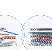
According to the structure of the 2D TMOs source matrix crystal, it is mainly divided into two types: layer structured and nonlayer structured TMOs [213]. Layer structured TMOs such as MoO3, WO3, Ga2O3, and V2O5 can exist naturally in the form of layered crystals in hydrate or anhydrous phase. In their corresponding 3D matrix, the atoms in-plane of the same layer are covalently bonded, and the layers are combined by weak interaction force between the stacking directions of the layers. These oxides can be exfoliated into nanosheets with oxygen terminated substrate surface by liquid or gas phase technology, which remain stable in air and water. These TMOs can be reduced to layers, the number of which is in the thinnest and most stable planar configuration, depending on their unit cell composition. Among them, binary metal trioxides have a layered structure with a general formula of MO3 (M = Mo, Ta, W, etc.) [206, 214]. For example, each layer in layered MoO3 (Figure 1.7a) is mainly composed of deformed MoO6 octahedrons in orthorhombic crystals [215]. The 2D layer is formed by octahedron and its neighbors sharing edges. The bulk crystal is formed by stacking the layers in turn along the y-axis by vdW force. Another typical layered TMO material is V2O5 (Figure 1.7b). The α-V2O5 is the most stable phase in the vanadium oxide family because it has the
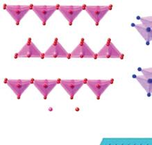


Figure 1.7 (a) Crystal structures of MoO3; (b) crystal structures of V2O5; (c) crystal structures of CeO2 Source: Reproduced with permission from Ref. [213], © Chemical Reviews 2017; (d) schematic drawing of the preparation of nonlayered structures into nanosheets. Source: Reproduced with permission from Ref. [215], © Nature Communications 2012.
highest vanadium oxidation state. It has a layered structure and a positive cross-cell structure during crystallization [216]. The monolayer consists of a twisted triangular biconical polyhedron with O atoms around V atoms. The polyhedron forms a (V2O4)n zigzag double chain along the direction (001), sharing edges and crosslinking edges along the direction (100), forming a 2D layer. The layers are also stacked together by vdW force to form bulk crystals.
Among the currently known TMO materials, only a few have a layered structure, and most of them are nonlayered structures in which atoms are connected by chemical bonds in the 3D direction of the crystal [217]. Some common nonlayer structured TMOs are CeO2, TiO2, In2O3, HfO2, and Fe2O3. Most of their crystal structures are different from each other, so there is no general formula [218]. CeO2 is one example of nonlayer structured TMOs. CeO2 has a fluorite structure and the space group is Fm3m (Figure 1.7c). Fluorite structure is formed on the basis of FCC unit cell, in which cations and anions occupy octahedral space. In the CeO2 structure, each Ce4+ ion coordinates with eight equivalent O2− nearest neighbors, while each O2− ion coordinates with four nearest neighbors Ce4+ [78]. There is no obvious natural delamination inside the crystal of the material, so it cannot be separated by methods such as micromechanical exfoliation. However, if the vertical chemical bonds inside the crystal are broken, the thickness of the crystal is reduced to an atomic size and a 2D plane with a certain lateral size appears, then 2D TMOs different from the corresponding parent crystal can be obtained (Figure 1.7d).
Compared with layer structured TMOs, nonlayer structured TMOs combine the advantages of an atomically thin structure and a highly active surface and also produce many new characteristics. When the structure of the material changes from a 3D bulk to a 2D layer with an atomic thickness of only a few nanometers, the sharp decrease in the thickness causes the distortion of the material lattice structure, and finally a stable structure with a lower surface energy is formed. The reconstruction of crystal structure will also lead to the change of energy band structure and electronic state [219]. Due to the breaking of the chemical bonds in the vertical direction of the 3D matrix, a large number of unsaturated dangling bonds are generated on the newly formed surface. Together with the strong surface polarization, a highly active surface with many active sites and a large specific surface area is formed [218], making it expected to have highefficiency catalytic ability and energy storage performance. In addition, the 2D planar structure makes 2D nonlayer structured TMOs compatible with microelectronic technology processing [220]. It can overcome the shortcomings of the high rigidity of traditional semiconductor materials such as silicon, making it expected to be widely used in the emerging flexible electronic fields such as wearable technology.
Different methods have been designed to synthesize 2D TMOs based on gas phase and liquid phase processes. It is still a challenging task to precisely synthesize inorganic planar crystals of one or more unit thickness during gas phase synthesis. Layer by layer epitaxy of two-dimensional films is classified as Frank van der Merwe growth [221]. For TMOs, the flux of adsorbed atoms and the lowest unfilled surface energy of the substrate on which the new material is deposited determine the occurrence of layer by layer oxide epitaxy [222]. For the physical deposition in the vapor phase, in a small period superlattice, one or more cell surfaces may grow
independently or in combination. The most common 2D TMO vapor phase techniques include CVD, MBE, atomic layer deposition (ALD), and pulsed laser deposition (PLD). In order to successfully deposit atomic-scale thin oxide layer or superlattice, it is necessary to precisely adjust deposition parameters. Especially in MBE, 2D deposition needs to significantly reduce the flux of adsorbed atoms, so it usually needs ultrahigh vacuum environment, which increases the complexity of equipment and deposition cost. Another problem is the influence of the substrate on the perfect deposition of oxides. The lattice matching and surface energy factors should be considered at the same time.
Many current 2D TMO synthesis techniques rely on liquid phase environments. Oxide epitaxial layers can be solvothermally grown in liquid solutions (at elevated temperatures) with or without a guiding agent [218, 223]. The carrier solvent can be water based and depends on the evaporation temperature of the solution, which may be necessary to be carried out in a pressurized container. The purity of the analyte and solvent plays an important role in the final result. Solution-based technology can be performed in one step, forming a layer directly on the substrate. Similar to the vapor deposition technique, it is important to consider the registration of the unit cell and the substrate or the layers near it for the nonscattering displacement and exchange of free carriers. The crystal orientation should be controlled at the cell level in these cases, and other quasi liquid methods may also be applied. The precursor of the material can be obtained by secondary processes such as spin coating, dip coating, or drop casting, such as oxygen annealing.
If the products synthesized in liquid or gas phase are layered crystals, the number of layers can be reduced by using the exfoliation step. These layered crystals can form different material patterns between TMO planes. After the exfoliation is completed, the pattern can be left to stabilize the oxide layer or be removed [224].
References
1 Castro Neto, A.H., Guinea, F., Peres, N.M.R. et al. (2009). The electronic properties of graphene. Reviews of Modern Physics 81: 109–162.
2 Novoselov, K.S., Geim, A.K., Morozov, S.V. et al. (2004). Electric field effect in atomically thin carbon films. Science 306: 666.
3 Schmidt, H., Giustiniano, F., and Eda, G. (2015). Electronic transport properties of transition metal dichalcogenide field-effect devices: surface and interface effects. Chemical Society Reviews 44: 7715–7736.
4 Duan, X., Wang, C., Pan, A. et al. (2015). Two-dimensional transition metal dichalcogenides as atomically thin semiconductors: opportunities and challenges. Chemical Society Reviews 44: 8859–8876.
5 Xie, L.M. (2015). Two-dimensional transition metal dichalcogenide alloys: preparation, characterization and applications. Nanoscale 7: 18392–18401.
6 Wang, Q.H., Kalantar-Zadeh, K., Kis, A. et al. (2012). Electronics and optoelectronics of two-dimensional transition metal dichalcogenides. Nature Nanotechnology 7: 699–712.
7 Chhowalla, M., Shin, H.S., Eda, G. et al. (2013). The chemistry of two-dimensional layered transition metal dichalcogenide nanosheets. Nature Chemistry 5: 263–275.
8 Butler, S.Z., Hollen, S.M., Cao, L. et al. (2013). Progress, Challenges, and Opportunities in Two-Dimensional Materials Beyond Graphene. ACS Nano 7: 2898–2926.
9 Xu, M., Liang, T., Shi, M., and Chen, H. (2013). Graphene-like two-dimensional materials. Chemical Reviews 113: 3766–3798.
10 Ci, L., Song, L., Jin, C. et al. (2010). Atomic layers of hybridized boron nitride and graphene domains. Nature Materials 9: 430–435.
11 Radisavljevic, B., Radenovic, A., Brivio, J. et al. (2011). Single-layer MoS2 transistors. Nature Nanotechnology 6: 147–150.
12 Zhang, H., Liu, C.-X., Qi, X.-L. et al. (2009). Topological insulators in Bi2Se3, Bi2Te3 and Sb2Te3 with a single Dirac cone on the surface. Nature Physics 5: 438–442.
13 Liu, Y., Weiss, N.O., Duan, X. et al. (2016). Van der Waals heterostructures and devices. Nature Reviews Materials 1: 16042.
14 Jariwala, D., Sangwan, V.K., Lauhon, L.J. et al. (2014). Emerging device applications for semiconducting two-dimensional transition metal dichalcogenides. ACS Nano 8: 1102–1120.
15 Huang, X., Zeng, Z., and Zhang, H. (2013). Metal dichalcogenide nanosheets: preparation, properties and applications. Chemical Society Reviews 42: 1934–1946.
16 Huang, X., Tan, C., Yin, Z., and Zhang, H. (2014). 25th anniversary article: hybrid nanostructures based on two-dimensional nanomaterials. Advanced Materials 26: 2185–2204.
17 Li, H., Wu, J., Yin, Z., and Zhang, H. (2014). Preparation and applications of mechanically exfoliated single-layer and multilayer MoS2 and WSe2 nanosheets. Accounts of Chemical Research 47: 1067–1075.
18 Chen, Y.L., Analytis, J.G., Chu, J.H. et al. (2009). Experimental realization of a three-dimensional topological insulator, Bi2Te3. Science 325: 178.
19 Zeng, M., Xiao, Y., Liu, J. et al. (2018). Exploring two-dimensional materials toward the next-generation circuits: from monomer design to assembly control. Chemical Reviews 118: 6236–6296.
20 Wang, H., Yuan, H., Sae Hong, S. et al. (2015). Physical and chemical tuning of two-dimensional transition metal dichalcogenides. Chemical Society Reviews 44: 2664–2680.
21 Fan, J., Li, T., and Djerdj, I. (2015). Two-dimensional atomic crystals: paving new ways for nanoelectronics. Journal of Electronic Materials 44: 4080–4097.
22 Parviz, B.A., Ryan, D., and Whitesides, G.M. (2003). Using self-assembly for the fabrication of nano-scale electronic and photonic devices. IEEE Transactions on Advanced Packaging 26: 233–241.