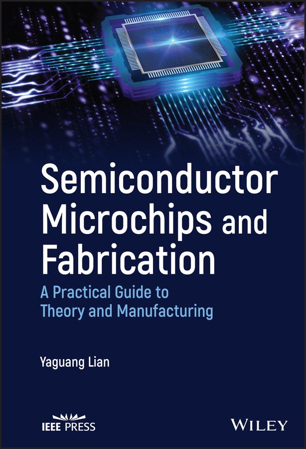
https://ebookmass.com/product/semiconductor-microchips-andfabrication-a-practical-guide-to-theory-and-manufacturing-
Instant digital products (PDF, ePub, MOBI) ready for you
Download now and discover formats that fit your needs...
Semiconductor Manufacturing Handbook, Second Edition Hwaiyu Geng [Geng
https://ebookmass.com/product/semiconductor-manufacturing-handbooksecond-edition-hwaiyu-geng-geng/
ebookmass.com
MASTER PLANNING AND SCHEDULING a practical guide to challenges in the current and future... competitive manufacturing world. 4th Edition John F Deutsch Eric Proud
https://ebookmass.com/product/master-planning-and-scheduling-apractical-guide-to-challenges-in-the-current-and-future-competitivemanufacturing-world-4th-edition-john-f-deutsch-eric-proud/ ebookmass.com
Flight Theory and Aerodynamics: A Practical Guide for Operational Safety 3rd Edition, (Ebook PDF)
https://ebookmass.com/product/flight-theory-and-aerodynamics-apractical-guide-for-operational-safety-3rd-edition-ebook-pdf/
ebookmass.com
Introduction to Diagnostic Microbiology for the Laboratory Sciences 1st Edition, (Ebook PDF)
https://ebookmass.com/product/introduction-to-diagnostic-microbiologyfor-the-laboratory-sciences-1st-edition-ebook-pdf/
ebookmass.com
General, organic, & biological chemistry Third Edition
Janice G. Smith
https://ebookmass.com/product/general-organic-biological-chemistrythird-edition-janice-g-smith/
ebookmass.com
Principles of Classroom Management: A Professional Decision-Making Model 7th Edition – Ebook PDF Version
https://ebookmass.com/product/principles-of-classroom-management-aprofessional-decision-making-model-7th-edition-ebook-pdf-version/
ebookmass.com
The Poetry of Emily Dickinson: Philosophical Perspectives Elisabeth Camp
https://ebookmass.com/product/the-poetry-of-emily-dickinsonphilosophical-perspectives-elisabeth-camp/
ebookmass.com
Climate Justice: Integrating Economics and Philosophy Ravi Kanbur
https://ebookmass.com/product/climate-justice-integrating-economicsand-philosophy-ravi-kanbur/
ebookmass.com
McGraw-Hill Education SAT Elite 2022 Christopher Black
https://ebookmass.com/product/mcgraw-hill-education-satelite-2022-christopher-black/
ebookmass.com
Glaucoma: A Neurodegenerative Disease of the Retina and Beyond: Part A Giacinto Bagetta (Editor)
https://ebookmass.com/product/glaucoma-a-neurodegenerative-disease-ofthe-retina-and-beyond-part-a-giacinto-bagetta-editor/
ebookmass.com
SemiconductorMicrochipsandFabrication IEEEPress
445HoesLane
Piscataway,NJ08854
IEEEPressEditorialBoard
SarahSpurgeon, EditorinChief
JónAtliBenediktsson
AnjanBose
AdamDrobot
Peter(Yong)Lian
AndreasMolisch
SaeidNahavandi
JeffreyReed
ThomasRobertazzi
DiomidisSpinellis
AhmetMuratTekalp
SemiconductorMicrochipsandFabrication APracticalGuidetoTheoryandManufacturing
YaguangLian
UniversityofIllinois Urbana,USA
Copyright©2023byTheInstituteofElectricalandElectronicsEngineers,Inc.Allrights reserved.
PublishedbyJohnWiley&Sons,Inc.,Hoboken,NewJersey.
PublishedsimultaneouslyinCanada.
Nopartofthispublicationmaybereproduced,storedinaretrievalsystem,ortransmittedinany formorbyanymeans,electronic,mechanical,photocopying,recording,scanning,orotherwise, exceptaspermittedunderSection107or108ofthe1976UnitedStatesCopyrightAct,without eitherthepriorwrittenpermissionofthePublisher,orauthorizationthroughpaymentofthe appropriateper-copyfeetotheCopyrightClearanceCenter,Inc.,222RosewoodDrive,Danvers, MA01923,(978)750-8400,fax(978)750-4470,oronthewebatwww.copyright.com.Requeststo thePublisherforpermissionshouldbeaddressedtothePermissionsDepartment,JohnWiley& Sons,Inc.,111RiverStreet,Hoboken,NJ07030,(201)748-6011,fax(201)748-6008,oronlineat http://www.wiley.com/go/permission.
LimitofLiability/DisclaimerofWarranty:Whilethepublisherandauthorhaveusedtheirbest effortsinpreparingthisbook,theymakenorepresentationsorwarrantieswithrespecttothe accuracyorcompletenessofthecontentsofthisbookandspecificallydisclaimanyimplied warrantiesofmerchantabilityorfitnessforaparticularpurpose.Nowarrantymaybecreatedor extendedbysalesrepresentativesorwrittensalesmaterials.Theadviceandstrategiescontained hereinmaynotbesuitableforyoursituation.Youshouldconsultwithaprofessionalwhere appropriate.Neitherthepublishernorauthorshallbeliableforanylossofprofitoranyother commercialdamages,includingbutnotlimitedtospecial,incidental,consequential,orother damages.
Forgeneralinformationonourotherproductsandservicesorfortechnicalsupport,please contactourCustomerCareDepartmentwithintheUnitedStatesat(800)762-2974,outsidethe UnitedStatesat(317)572-3993orfax(317)572-4002.
Wileyalsopublishesitsbooksinavarietyofelectronicformats.Somecontentthatappearsin printmaynotbeavailableinelectronicformats.FormoreinformationaboutWileyproducts, visitourwebsiteatwww.wiley.com.
LibraryofCongressCataloging-in-PublicationDataAppliedfor: HardbackISBN:9781119867784
CoverDesign:Wiley
CoverImage:©DenRise/Shutterstock
Setin9.5/12.5ptSTIXTwoTextbyStraive,Chennai,India
Contents
AuthorBiography xi
Preface xiii
1IntroductiontotheBasicConcepts 1
1.1WhatIsaMicrochip? 1
1.2Ohm’sLawandResistivity 1
1.3Conductor,Insulator,andSemiconductor 5 References 5
2BriefIntroductionofTheories 7
2.1TheBirthofQuantumMechanics 7
2.2EnergyBand(Band) 11 References 15
3EarlyRadioCommunication 17
3.1TelegraphTechnology 17
3.2ElectronTube 19 References 22
4BasicKnowledgeofElectricCircuits(Circuits) 23
4.1ElectricCircuitsandtheComponents 23
4.2ElectricField 26
4.3MagneticField 28
4.4AlternatingCurrent 30
5FurtherDiscussionofSemiconductorsandDiodes 33
5.1SemiconductorEnergyBand 33
5.2SemiconductorDoping 36
5.3SemiconductorDiode 42 References 46
6TransistorandIntegratedCircuit 47
6.1BipolarTransistor 47
6.2JunctionFieldEffectTransistor 49
6.3Metal–SemiconductorFieldEffectTransistor 52
6.4Metal–Insulator–SemiconductorFieldEffectTransistor 55 References 60
7TheDevelopmentHistoryofSemiconductorIndustry 61
7.1TheInstructionofSemiconductorProductsandStructures 61
7.2ABriefHistoryoftheSemiconductorIndustry 63
7.3ChangesintheSizeofTransistorsandSiliconWafers 65
7.4CleanRoom 67
7.5PlanarProcess 71 References 75
8SemiconductorPhotonicDevices 77
8.1Light-EmittingDevicesandLight-EmittingPrinciples 77
8.2Light-EmittingDiode(LED) 82
8.3SemiconductorDiodeLaser 88
8.3.1ResonantCavity 89
8.3.2ReflectionandRefractionofLight 91
8.3.3HeterojunctionMaterials 93
8.3.4PopulationInversionandThresholdCurrentDensity 94 References 96
9SemiconductorLightDetectionandPhotocell 97
9.1DigitalCameraandCCD 97
9.2Photoconductor 100
9.3TransistorLaser 101
9.4SolarCell 105 References 106
10ManufactureofSiliconWafer 109
10.1FromQuartziteOretoPolysilicon 110
10.2ChemicalReaction 113
10.3PullSingleCrystal 115
10.4PolishingandSlicing 116 References 123
11BasicKnowledgesofProcess 125
11.1TheStructureofIntegratedCircuit(IC) 125
11.2ResolutionofOpticalSystem 128
11.3WhyPlasmaUsedintheProcess 131 References 133
12Photolithography(Lithography) 135
12.1TheStepsofLithographyProcess 135
12.1.1Cleaning 135
12.1.2DehydrationBake 136
12.1.3PhotoresistCoating 138
12.1.4SoftBake 141
12.1.5AlignmentandExposure 141
12.1.6Developing 145
12.1.7Inspection 146
12.1.8HardBake 147
12.1.9Descum 148
12.2AlignmentMark(Mark)DesignonthePhotomask 152
12.3ContemporaryPhotolithographyEquipmentTechnologies 156 References 159
13DielectricFilmsGrowth 161
13.1TheGrowthofSiliconDioxideFilm 162
13.1.1ThermalOxidationProcessofSiO2 162
13.1.2LTOProcess 164
13.1.3PECVDProcessofSiliconDioxide 166
13.1.4TEOS + O3 DepositionUsingAPCVDSystem 167
13.2TheGrowthofSiliconNitrideFilm 168
13.2.1LPCVD 168
13.2.2PECVDProcessofSiliconNitride 171
13.3AtomicLayerDepositionTechnique 174 References 177
14IntroductionofEtchingandRIESystem 179
14.1WetEtching 179
14.2RIESystemforDryEtching 182
14.2.1RIEProcessFlowandEquipmentStructure 182
14.2.2ProcessChamber 184
14.2.3VacuumPumps 186
14.2.4RFPowerSupply(Source)andMatchingNetwork(Matchwork) 187
14.2.5GasCylinderandMassFlowController(MFC) 189
14.2.6HeaterandCoolant 194
References 196
15DryEtching 197
15.1TheEtchProfileofRIE 197
15.1.1Case1 198
15.1.2Case2 201
15.2EtchingRateofRIE 203
15.3DryEtchingofIII–VSemiconductorsandMetals 206
15.4EtchProfileControl 207
15.4.1InfluenceofthePROpeningShapeontheEtchProfile 208
15.4.2TheEffectofCarbononEtchingRateandProfile 209
15.5OtherIssues 211
15.5.1TheDifferencesBetweenRIEandPECVD 211
15.5.2TheDifferenceBetweenSiandSiO2 DryEtching 214
15.6InductivelyCoupledPlasma(ICP)TechniqueandBoschProcess 215
15.6.1InductivelyCoupledPlasmaTechnique 216
15.6.2BoschProcess 219
References 223
16MetalProcesses 225
16.1ThermalEvaporationTechnique 225
16.2ElectronBeamEvaporationTechnique 227
16.3MagnetronSputteringDepositionTechnique 231
16.4TheMainDifferencesBetweenElectronBeam(Thermal)Evaporation andSputteringDeposition 234
16.5MetalLift-offProcess 235
16.6MetalSelectionandAnnealingTechnology 241
16.6.1TheSelectionofMetals 241
16.6.2MetalAnnealing 242
References 243
17DopingProcesses 245
17.1BasicIntroductionofDoping 245
17.2BasicPrinciplesofDiffusion 246
17.3ThermalDiffusion 247
17.4DiffusionandRedistributionofImpuritiesinSiO2 248
17.5MinimumThicknessofSiO2 MaskingFilm 250
17.6TheDistributionofImpuritiesUndertheSiO2 MaskingFilm 251
17.7DiffusionImpuritySources 252
17.8ParametersoftheDiffusionLayer 255
17.9Four-PointProbeSheetResistanceMeasurement 256
17.10IonImplantationProcess 257
17.11TheoreticalAnalysisofIonImplantation 259
17.12ImpurityDistributionafterImplantation 260
17.13TypeandDoseofImplantedImpurities 262
17.14TheMinimumThicknessofMaskingFilm 263
17.15AnnealingProcess 264
17.16BuriedImplantation 266
17.16.1ImplantationthroughMaskingFilm 266
17.16.2SOIManufacture 267
References 270
18ProcessControlMonitor,Packaging,andtheOthers 271
18.1DielectricFilmQualityInspection 271
18.2OhmicContactTest 273
18.3Metal-to-MetalContact 274
18.4ConductiveChannelControl 277
18.5ChipTesting 278
18.6Dicing 279
18.7Packaging 280
18.8EquipmentOperationRange 281
18.9Low-k andHigh-k Dielectrics 282
18.9.1CopperInterconnectionandLow-k Dielectrics 283
18.9.2QuantumTunnelingEffectandHigh-k Dielectrics 286
18.10End 291
References 293
Index 295
AuthorBiography YaguangLian isaresearchengineerinHolonyak Micro&NanotechnologyLabattheUniversityof IllinoisatUrbana-Champaign(UIUC).In1979,he studiedattheDepartmentofElectronics,Hebei University,China.In1983,withabachelor’s degree,heworkedonsiliconepitaxyforasemiconductorcompanyfortwoyears.Yaguangreturned toHebeiUniversityasagraduatestudentin1985. In1988,hegothismaster’sdegree.From1988 to2001,heworkedwithHebeiSemiconductor ResearchInstitute(HSRI).In2001,Yaguang joinedastart-upcompanyatCaliforniaasasenior semiconductorprocessengineer.Twoyearslater, heworkedintheUniversityofCalifornia,LosAngeles(UCLA).FromNovember 2004tillnow,YaguangworksasresearchengineerattheUniversityofIllinois.
Withover35yearsofexperienceinthesemiconductorfield,Yaguanghas dealtwithdifferentprocessesfordifferentkindsofsemiconductors,suchasSi andGaAs.WhenheworkedinHSRIinChina,hewasmanufacturingGaAs MESFETdigitalICanddesigningcircuits,andalsomanagedaprocessflowfrom implantationtopackaging.InthecompanyatCalifornia,heworkedmainlyin themanufactureofsiliconopticalwaveguide.AtUCLA,Yaguangstartedthe equipmentrepairandmaintenance,andusers’training,whichhefurtherevolved atUIUC.Heisalsoresponsiblefordesigningdifferentrecipestomeettheneeds ofprofessorsindifferentprojects,suchasdryetchingofsilicon,III–Vmaterials, dielectricfilmsandmetals,anddepositionofsiliconnitridefilmwithdifferent
xii AuthorBiography
stresses.Hesolvesdifferenttypesofprocessproblemsforstudentspavingwayfor theirresearch.
Yaguangbelievesthattobeagoodengineer,onemusthaveanimportanttrait, whichis“itisnotenoughforyoutoknowhowtodoit,youmustknowwhy todoit.”
Preface “Semiconductorprocessengineer”isthelabelofmywholecareer.Asaresearch engineer,IhavebeenworkinginHolonyakMicro&NanotechnologyLaboratory (HMNTL)attheUniversityofIllinoisfornearlytwodecades.Thecorepartof HMNTListhecleanroomwithdifferenttypesofequipment,whichareused tofabricatevarioussemiconductordevices.Thelabisopentothecampusand society.Uptonow,Ihavetrainedthousandsofusersinusingthelabmachines. Mostusersaredoctoralstudents.Thesetrainingexperienceshavegivenmethe opportunitiestoencountervariousissuesandsolvedifferenttechnicalproblems withdifferentkindsofusers.
Duringmyyearsoftraining,Ihavemetstudentswithdifferentbackgrounds. MostofthemhaveEEorECEbackgrounds,andsomeofthemdon’thavethese backgrounds.ThestudentwithoutEEorECEbackgroundslackbasicknowledge ofsemiconductorsandprocessing,whilestudentsmajoringinEEorECEneedto makeuptheworkingprinciplesofmanufacturingprocessesandthebasicstructuresofequipment.Lackofadequateunderstandingofprocessandequipment notonlyoccursinmanydoctoralstudentswithbackgroundsinEEorECE,but alsoinsomepostdoctoralresearchers.Animportantreasonforthisphenomenon isthattheydonotunderstandtheprocessandequipmentfromtheperspective ofphysicalandchemicalprinciples.Theseissuesandtheencouragementfrom studentsdrovemetowritethisbook.
Weareusingmicrochipstodescribesemiconductordevicesandintegrated circuits(ICs).TomeettheneedsofreaderswithoutEEorECEbackgrounds, thisbookincludestheknowledgeofsemiconductorconcepts,theories,histories, andbasicstructuresofmicrochips,whichhelptolaythefoundationforthemto understandsemiconductormanufacturingprocesses.Tohelpthereaderswith EEorECEbackgroundsbetterunderstandtheprocessandequipment,thisbook strivestoclarifytheprinciplesofprocesses,thebasicstructuresofequipment,and thedesignofprocessrecipesbasedonthephysicallaws,chemicalreactions,and electricalcircuittheories.Itnotonlyshowsreadershowtodotheprocess,but alsoexplainswhytheprocessisdesignedinsuchaway.Itcombinestheprocesses
Preface
withtheactualmachinesusedinthecleanroomattheUniversity.Therefore,the bookwillbeveryusefulforreaderswithdifferentbackgrounds.
Thisisahandybookformanyaudiencesasitstartswiththebasicconcepts anddailyexamples.Itusessimplelanguagetoexplaincomplicatedconcepts andtheories.Theneedsofvariouslevelsofaudienceswillbesatisfied,suchas undergraduates,graduates,researchers,engineers,andprofessors.Thebookwill pavethewaysforreadersintheirsemiconductorresearch,process,andmanufacture.Fromthisbook,readerscanfindmanyvaluablesuggestionsandsolutions totheproblemsthatstudentsorengineersoftenencounterinsemiconductor processing.Thesesuggestionsandsolutionsarebasedonmyyearsofworking experience.Moreover,readerscanalsofindsomeusefulexperimentalresultsin thebook,whichwillhelpthemintheirprocessingwork.
Nowadays,semiconductorsarewidelyusedinmanyfields.Thisbookis alsowrittenforthosewhoarenotmajoringbutinterestedintheresearchand productionofsemiconductormicrochips.Eventhosewhodonothaveenough knowledgeofsemiconductorandprocesses,aslongastheyhavebasicknowledge ofphysics,chemistry,andcircuit,afterreadingthisbook,caneasilylearnand quicklygrasptheprinciples,knowledge,andmanufacturingprocessesofsemiconductors.Fromthisbook,readerscanobtainthefundamentalconceptsand skills,whichwillbeanecessityinthedevelopmentofsemiconductorprocessing. Theycanapplyalltheseconceptsandskillsinsemiconductortechnologyto improvetheirproductqualityortheprojectresearch.
IcouldnotaccomplishmybookwithoutHMNTL.InHMNTL,Ihavegotten agoodtimewithmycolleagues.Iwouldliketoexpressmyappreciationtomy excellentcolleagues:Mr.JohnHughes,Dr.MarkMcCollum,Dr.EdmondChow, Dr.GlennysMensing,KenTarman,HalRomans,MichaelHansen,Lavendra Mandyam,KarthickJeganathan,PaulDiPippo.Fromthem,Ihavelearnedmore aboutthelayoutandmanagementofthecleanroomattheuniversity.Fromthem, Ialsohavegottenalotofhelpintheequipmenttroubleshooting,recipedesign,and parametertesting.IamsogladthatIhaveworkedwiththemforsomanyyears.
Inwritingthisbook,manyfriendshaveofferedtheirsupport.Dr.RuijieZhao gavemegoodadviceatthebeginning.Dr.WenjuanZhureviewedthedraft. Dr.AnmingGaopushedmetowritethebook.Mr.RamanKumarandAlvin Floresprovidedmegoodsuggestionsonsometheoreticalissues,andsome studentssuppliedmewithniceimages.IespeciallythankTianyiBai,mynephew, agraduatestudentattheUniversityofPennsylvania,whohasgivenmevaluable opinionsinsomeareas.Finally,IwouldliketothanktheInternet,whichwas bornfromsemiconductortechnology.FromtheInternet,Icaneasilyfindthe informationIneed.Here,Ideeplyappreciatethecompaniesandindividualswho agreedtoletmeusetheirimagesinthebook.
February12,2022 YaguangLian
UniversityofIllinoisatUrbana-Champaign Champaign,IL
IntroductiontotheBasicConcepts 1.1WhatIsaMicrochip? Lookingbackonthedevelopmenthistoryofhumansociety,ithasgonethrough differentstagesofcivilization,fromtheprimitivestoneagetothemoderninformationage.Thematerialusedtosupportstoneagewasstone.Thematerialused tosupportinformationageissemiconductor.Socontemporarysocietyisessentiallyasemiconductorerarepresentedbysilicon.Thiserabeganinthelate1950s andearly1960sintheBayAreaofNorthernCalifornianearSanFranciscointhe UnitedStates.Later,peoplecalledthisarea“SiliconValley,”thesignofhightechnology(abbreviatedtohigh-tech),whichhavebroughtusintotheinformationage. Siliconandothersemiconductorsarethecornerstoneofthisera.Ifpetroleumis thoughtasthebloodofmodernsociety,semiconductormicrochipscanberegarded asthebrain.Semiconductortechnologyhasbeenintegratedbydifferentindustriestoenhancetheirtechnicallevel,andithasalsocomeintoourhouseholds.A microchipisasemiconductordeviceoranintegratedcircuit(IC).AnICistomake alotoftinysemiconductordevicesontoasmallflatpieceofsemiconductor(adie).
1.2Ohm’sLawandResistivity Duetomicrochipsareoperatedbyelectricity,sofirst,letusgettoknowwhatelectricityis,andhowelectricityworks.SeeFigure1.1.Itisavoltageconverterfora smallhouseholdelectronicproduct.Theexplanationofsometechnicalwordson theconverterarelistedasfollows:
● “VAC”means“VoltsAlternatingCurrent”
● “Hz-Hertz”isthefrequencyunit
● “W-Watt”istheunitofpower
● “mA”means“milli-Ampere.”“Ampere-A”istheunitofelectriccurrent(abbreviatedtocurrent)
SemiconductorMicrochipsandFabrication:APracticalGuidetoTheoryandManufacturing, FirstEdition.YaguangLian.
©2023TheInstituteofElectricalandElectronicsEngineers,Inc.Published2023byJohnWiley&Sons,Inc.
Figure1.1 Avoltageconverterforan electronicproduct.Source:Harman InternationalIndustries,Incorporated.
Amongthem,voltage,current,andwattarethethreebasicparametersusedto expressthecharacteristicsofelectricity.Anotherbasicparameterisresistance,we willtalkaboutitinOhm’slawbelow.
Electricityisthesetofphysicalphenomena.Aphysicalphenomenonreferstoa processthatdoesnotproducenewsubstances,suchasthemovementofobjects, thefreezingandboilingofwater,andsoon.Correspondingtothisisachemicalphenomenon,whichreferstoaprocessthatcanproducenewsubstances.We callthisprocessachemicalreaction,forexample,oxygenandhydrogengenerate waterthroughachemicalreaction.Thereisalsoanuclearphenomenon,which isbeyondthescopeofthisbookandwillnotbediscussed.Now,letusreturnto thetopicofelectricity.Electricityisgeneratedbythemotionofmatterthathasa propertyofelectriccharge.Anelectricchargecanbepositiveornegative.Positiveoneiscalled“positivecharge”andrepresentedby“+.”Negativeoneiscalled “negativecharge”andrepresentedby“ .”Themovementofelectricchargesis anelectriccurrent.Inmostcases,thecurrentisproducedbythemovementof electrons,whicharenegativecharges.Theunitofelectriccurrent,Ampere,is namedinhonorofaFrenchmathematicianandphysicistAndré-MarieAmpère (1775–1836),whoisconsideredthefatherofelectrodynamics.
Electricitycomesintoourhomesthroughelectricalwiresandthengoestovariouselectricalappliances.Thereareusuallytwokindsofelectricalwires(abbreviatedtowire)forhouseholduse.Theyaretwo-corewires,justlikethewireattached totheconverterinFigure1.1,andthree-corewires.Ifwestripathree-corewire, itsstructureisshowninFigure1.2.“CableJacket”istheinsulatingsheath,“Wire Insulation”istheinsulatinglayer,and“StrippedWire”isthewireexposedafter
Figure1.2 Thebasicstructureofthree-core wire.
theinsulatinglayerisstripped.Thethreewiresarehot,neutral,andground.Most oftheinsulatingsheathesandlayersaremadeofrubberandplastic;thewireis madeofmetal.Inmostcases,themetalisaluminumorcopper.Thekindofmaterialssuchasrubberandplasticarecalledinsulators,inwhich,electronscannot move.Thus,currentcannotflowintheinsulators.Wecallaluminumandcopper,thetypeofmaterials,conductors,becauseelectronscanmoveinthem.Thus, electricalcurrentcanflowintheconductors.
Allmaterialsarecomposedofatoms,andatomswillhinderthemovementof electrons,whichmeansthatallmaterialshaveresistanceintheoppositedirectionofthecurrentflow.Thisresistanceiscalledelectricalresistance(abbreviatedtoresistance),andtheunitoftheresistanceisOhm,whichisrepresentedby “Ω.” Ω isnamedinhonoroftheGermanphysicistGeorgSimonOhm(March16, 1789–July6,1854).Howdoelectronsmoveinaconductortogeneratethecurrent? Theyaredrivenbythepressureofelectricity.Thisspecialpressureiscalledvoltage, andtheunitisvolt,whichisexpressedby“V.”ThevoltageunitvoltistocommemoratetheItalianphysicistAlessandroVolta(1745–1827),whoinventedvoltaicpile, thefirstelectricalbatteryintheworld.Now,wehavethreeparametersrelated toelectricity:current,representedby“I ”;resistance,representedby“R”;voltage, representedby“V .”Sometimeslowercaselettersarealsousedtoindicatecurrent, resistance,andvoltage.TherelationshipbetweenthemisthefamousOhm’slaw:
Whycanelectronsflowinmetal?Itisbecausethemetalhaslittleresistance; electronscannotflowintheinsulatorbecausetheinsulatorhaslargeresistance. Scientistsuseresistivitytoexpresstheresistanceofamaterialperunitlength. “ ��”isusedtorepresentresistivity,itsunitisohm ⋅ cm(Ω ⋅ cm).Therelationship betweenresistanceandresistivityisexpressedbythefollowingformula:
Figure1.3 Adiagramofasectionofresistivematerial,currentflowsalongthelength direction.Source:ReproducedwithpermissionofPhysicsLibreTexts.
SeeFigure1.3,where“A”isthecross-sectionalarea,and“L”isthelengthof apieceofmaterial.Tomakemoreconvenientforpracticaluse,weintroducethe conceptofconductance.Thesymbolofconductanceis G,andtherelationship withresistance R isasfollows:
Theunitof G isSiemensandisrepresentedbytheletterStocommemorate WernervonSiemens(December13,1816–December6,1892).HewasaGerman scientistandfounderofSiemens.Correspondingly,thereisconductivity,expressed by �� ,andtherelationshipwithresistivity �� is
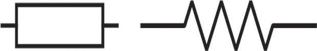
Inpracticalapplication,weoftenusedevicescalledresistors,whichareshown intheleftofFigure1.4,andthesymbolisshownintherightofFigure1.4.
Figure1.4 Thepictureofresistors(a)andthesymbol(b).Source:Reproducedwith permissionofSparkFunElectronics.
1.3Conductor,Insulator,andSemiconductor Now,weuseresistivitytodistinguishconductorsandinsulators.Ingeneral,the resistivityofaconductorisverylow,andtheresistivityofaninsulatorisveryhigh. Forexample,theresistivityofcopperis1.55 × 10 6 Ω cm,andforaluminumis
2.5 × 10 6 Ω cm[1],where10 6 isonemillionth.Polyvinylchloride(PVC)isa kindofplasticcommonlyusedformakinginsulatingmaterials,itsresistivityis
2 × 10¹² –2 × 10¹⁴ Ω ⋅ cm,nylonis4.56 × 1016 Ω ⋅ cm[2].Mathematically,102 means thereisazeroafter10,103 meanstherearetwozerosafter10,andsoon.From which,wecanknowthattheresistivityoftheabovetwoinsulatingmaterials has11–15zerosafter10.Conductorsandinsulatorshavetheresistivitieseither extremelysmallorextremelylarge.Doesamaterialwithresistivitybetweenthem exist?Yes,thismaterialexists,wecallitasemiconductor.Atroomtemperature,the resistivityofsiliconis6.3 × 104 Ω ⋅ cm,andtheresistivityofgermaniumis46 Ω ⋅ cm [1].SiliconwiththesymbolSiisthemostimportantmaterialinthemodern semiconductorindustry.ThatiswhytheBayAreaofNorthernCaliforniaiscalled SiliconValley.GermaniumwiththesymbolGewasusedtomakethefirsttransistorintheworld.Siliconandgermaniumaresingle-elementsemiconductors. Anotherkindofsemiconductorsarecompoundsemiconductors.Themostused oneisgalliumarsenidewithsymbolGaAs,whichhasaresistivityof107 –109 Ω cm [3].Withsuchahighresistivity,wecallthismaterialasemi-insulator.Duetothe highresistivity,pureGaAscannotbeusedtomakeadevice.Itmustbechanged toasemiconductorbyaprocessofdoping.Infact,siliconalsoneedstobedoped tomakedevices.WewilldiscussdopingprocessinChapter17.
Sofar,byusingtheresistivity,wehavedistinguishedbetweenconductors, semiconductors,semi-insulators,andinsulators.Generally,semi-insulating materialsrepresentedbyGaAsneedtobeconvertedintosemiconductorsbefore theycanbeusedtomakedevices.So,inthefollowingdiscussion,wewillclassify semi-insulatingmaterialsassemiconductors.Itistoosimpletodistinguish materialsfromresistivity.Toreallyunderstandthem,especiallysemiconductors, wehavetousequantummechanicsandenergybandtheory.Itisnecessaryforus togiveabriefintroductionofquantummechanicsandenergybandtheory.
References
1 饭田修一等,(1979). 物理学常用数表,[日]. 科学出版社,133–135.
2 Fink,D.G.andBeaty,H.W.(1987). StandardHandbookforElectricalEngineers, 12e,4–153.McGraw-HillCompanies.
3 Soares,R.,Graffeuil,J.,andObrégon,J.(1983). ApplicationsofGaAsMESFETs, 17.ArtechHouse.
Thischapterisabriefintroductionofquantummechanics,andthenenergyband theory.Byusingthesetheories,wecaneasilyunderstandwhatisaconductor,an insulator,andasemiconductor.
2.1TheBirthofQuantumMechanics Attheendofthenineteenthcenturyandthebeginningofthetwentiethcentury,Newtonianmechanics,Maxwell’stheoryoftheelectromagneticfield,and Maxwell–Boltzmannstatisticsconstitutedwhatisnowcalledclassicalphysicsthat ruledthephysicalworldatthattime.Thephysicalquantitiesdiscussedinclassicalphysicshavetwocharacteristics:continuityandcontrollability.However,there weretwoproblemsthatcouldnotbesolvedbyusingthetheoryofclassicalphysics. Onewasblackbodyradiation,andtheotherwasMichelson–Morleyexperiment. In1900,MaxPlanck(April23,1858–October4,1947),aGermantheoreticalphysicistproposedthatintheradiationandabsorptionofelectromagneticfield,the energyappearedinadiscreteratherthancontinuousform.Thisdiscreteenergy iscalledthequantizationofenergy.Thisassumptionexplainsblackbodyradiationverywellandisconsideredasthebeginningofquantummechanics.In1905, AlbertEinstein(March14,1879–April18,1955)publishedthetheoryofspecialrelativitytoexplainMichelson–Morleyexperiment.Sincethen,physicshasentered thepost-Newtonianeraofmodernphysics.
AccordingtoPlanck’sassumption,eachpartofenergyisproportionaltothe frequencyofelectromagneticradiation.Weuse E torepresenttheenergyand �� to representthefrequency.ThePlank’sequationis
E = h��
(2.1)
The“h”hereiscalledPlanck’sconstant.Thefrequencyisthenumberofoccurrencesofarepeatingeventperunitoftime.Inmostcases,frequencyisrepresented
SemiconductorMicrochipsandFabrication:APracticalGuidetoTheoryandManufacturing, FirstEdition.YaguangLian.
©2023TheInstituteofElectricalandElectronicsEngineers,Inc.Published2023byJohnWiley&Sons,Inc.
bytheletter“f .”However,inquantummechanicsitisrepresentedby“ν.”“T ”is usedtorepresenttheperiod.Itisthedurationoftimeofonecycleinarepeating event.Therelationshipbetween f and T isasfollows:
Ifweusesecondstoexpresstime,thenunitoffrequencyisHertz(Hz),named afterGermanphysicistHeinrichHertz(February22,1857–January1,1894).He usedtheexperimenttoconfirmtheexistenceofelectromagneticwaves.ElectromagneticwavesweretheoreticallypredictedbyJamesClerkMaxwell(June13, 1831–November5,1879).Thetheoryiswell-knownasMaxwell’sequations.The experimentalsoprovedthatthelightiselectromagneticwavesthatwerepredicted byMaxwell.
Planck’sEq.(2.1)playsaveryimportantroleinphysics.Itisoneofkeydifferencesbetweenclassicphysicsandmodernphysics.Inclassicphysics,theenergyis supposedtoexistinthecontinuousformandisvalidatalarge(macroscopic)scale. ThePlanckequationpointsoutthatatsmall(microscopic)scale,energyexistsin thediscrete(quantum)form,whichisoneofthebasiccharacteristicsofquantum mechanics.Therefore,whendealingwithmicroscopicworldssuchasatomsand subatomicparticles,wemustusequantummechanics.
In1905,Einsteinpublishedfourpapers–photoelectriceffect,Brownianmotion, specialtheoryofrelativity,andmass–energyequivalence.Thesefourarticlescontributedsubstantiallytothefoundationofmodernphysicsandchangedpeople’s viewsfrombeginningofhistoryonspace,time,mass,andenergy.Sothisyearis alsocalledthe“miracleyear”ofphysics.Inthepaperofmass–energyequivalence, Einsteinwrotedownawell-knownequation:
Inthisequation, E isenergy, m ismass, c isthespeedoflight, c = 300000km/s. Now,letustalkaboutphotoelectriceffect.Theeffectmeansthatwhenlight beamsshineonthesurfaceofanobject(mostlymetal),andifthelightfrequency ishigherthanacertainnumber,theelectronsonthesurfacewillbeexcited andescapefromtheobject.ThisphenomenonwasfirstdiscoveredbyHertz. Theescapedelectronsarecalledphotoelectrons.Inthepaperofphotoelectric effect,Einsteinassumedthatlighttravelthroughspace,notintheformofwaves asdescribedintheclassicaltheoryofelectromagneticfield,butindiscrete “wavepackets.”Awavepacketiscalleda“photon.”AphotonobeysPlanck’s equationandhasenergyof h�� .Whenthefrequency(energy)ofphotonsthatare illuminatingtheobjectreachesorexceedsacertainthresholdfrequency,electrons willbeemittedoutofthesurfaceoftheobject(seeFigure2.1).
In1913,NielsBohr(October7,1885–November18,1962),aDanishphysicist, andErnestRutherford(August30,1871–October19,1937),aBritishphysicistborn
E = mc2
(2.3)
Figure2.1 Theschematicdiagramofphotoelectriceffect.Source:Reproducedwith permissionofScienceABC.WhatisthePhotoelectricEffect? ≫ ScienceABC.
inNewZealand,togetherproposedamodeltodescribeatoms.Thismodelstates thatanatomcontainssmall,high-densitynucleus,surroundedbyelectrons.This islikethestructureofthesolarsystem,exceptthatthisattractioncomesfromelectromagneticforceratherthangravity.WecallthismodelRutherford–Bohrmodel, orsimplyBohrmodel.Figure2.2isBohrmodelofahydrogenatom.Inthisfigure, thenucleusisinthecenter,whichiscomposedofaneutronandaproton.Anelectronrotatesinouterorbits.Neutronisunchargedandprotonispositivelycharged. Sincethenumberofprotonsinanatomisthesameasthenumberofelectrons,
Figure2.2 Bohrmodelofahydrogenatom.(a)Aphotonisabsorbedandanelectron jumpsfromaninnerorbittoanouterorbit.(b)Anelectronjumpsfromanouterorbitto aninnerorbitandaphotonisemitted.Source:[1]Bertolotti/Taylor&Francis.
10
2BriefIntroductionofTheories undernormalcircumstances,theatomisnotchargedandisneutral.Thehydrogen atomiscomposedofanucleusandanelectron.
Inthismodel,theelectronisusuallyonaninnerorbit.Thisorbithasthelowest energyandiscalledthegroundstate(level).Butwhentheelectronabsorbsenough energy,itjumpstoanouterorbit(higherenergy),asshowedin(a).Theouter orbitiscalledanexcitedstate.Theexcitedstatecanhavemanystateswithdifferentenergyorbits,andwhichorbittheelectronjumpstodependsonhowmuch energyitabsorbs.Theelectronisunstableintheexcitedstates.Itwilljumpback tothelowerenergyorbitandreleaseitsenergybyemittingaphoton,asshowedin (b).Sometimes,wecanuse ΔE = h�� torepresenttheemittedphoton.“Δ”usually meansdifferenceinmathematics.Figure2.3isaschematicdiagramoftheenergy levelsofasiliconatom.Siliconiscomposedof1nucleusand14electrons.The nucleuscontains14protonswithpositivecharge.The“shell”inthefiguremeans thattheelectronsmovesofastthatanelectroncloudisformedaroundthenucleus, justlikeashell.Valenceelectronsaretheelectronslocatedinoutermostorbit.Ionizedlevelreferstoastatewhereanelectronhasabsorbedenoughenergytogetrid ofthebondageofthenucleusandbecomeafreeelectron.Inthiscase,theneutralityofanatomisbroken.Theremainingatombecomespositivecharge.Such atomsarecalledpositivelychargedions(positiveions).Theelectronsinphotoelectriceffectareionizedelectrons.Asmentionedabove,electronstendtooccupy thelow-energylevels,whicharetheshell1andshell2asshowninthefigure.They aretheinnershells.Theelectronsfullyoccupythestatesinthesetwoshells.The
Figure2.3 Bohrmodelofasiliconatom.Source:Adaptedfrom“HyperPhysics”of GeorgiaStateUniversity.
2.2EnergyBand(Band) 11
electronsatthesetwolevelsarestable.Inshell3,thenumberofelectronsisless thanthenumberofstatesinthislevel,soelectronscannotcompletelyoccupythe states.Theelectronsinthislevelarevalenceelectronsthatdeterminethechemicalpropertiesofsubstance.Theyparticipateinchemicalreactionandareeasily excitedtohigher-energystates.Siliconhasfourvalenceelectrons,andgermanium alsohasfour.
BasedontheworksofPlanck,Einstein,andBohr,ErwinSchrödinger(August 12,1887–January4,1961),anAustrianphysicist,publishedSchrödingerequation in1926.Sofar,quantummechanicshadbeeninitiallyestablished.
2.2EnergyBand(Band) ThephotoelectriceffectandBohrmodelimplyanimportantcharacteristicofelectrons,thatis,theyonlyoccupysomespecialenergylevels.Inthecaseofasingle atom,theseenergylevelsarediscrete.Butinacrystalmaterial,suchassilicon, discreteenergylevelsbecomeenergybands.Matterusuallyhasthreestates,solid, liquid,andgas.Thebranchofphysicsthatisthestudyofsolidsiscalledsolid-state physics.Ifasolidhasaperiodicandrepeatingstructure,itisacrystallinesolid (singlecrystalmaterial).Thesemiconductorsweareusingtomakemicrochips aremainlycrystallinesolids.Siliconhasasingle-atomstructure.Insiliconcrystals,atomsarearrangedperiodicallyandorderly.Figure2.4isaschematicdiagramofsiliconcrystalstructure.Thesmallballsinthefigurerepresentsilicon atoms,and X –Y –Z isthecoordinatesystem.Becausetheatomsareveryclosein thecrystal,thevalenceelectronsinanatomappeartobesharedbyotheratoms. Therefore,thediscreteenergylevelsofelectronsinasingleatombecomeenergy
Figure2.4 Schematic diagramofasilicon crystal.
bandsinacrystalmaterial.Usingthisviewandextendingquantummechanicsto solid-statephysics,oneoftheresultsobtainedisenergybandtheory.Bysolving theSchrödingerequation,thebandstructuresofdifferentcrystallinesolidscan beobtained.
Differentcrystalmaterialshavedifferentenergybandstructures,buttheyall haveonethingincommon.Someenergybandsallowelectronstooccupy,and someenergybandsprohibitelectronstooccupy.Energybandsthatprohibitelectronicoccupationarecalledforbiddenbands.Energybandsthatallowelectronic occupationaredividedintotwocategories:valanceband(fullband)andconductionband(emptyband).Accordingtothetheoryofsolid-statephysics,adjacent atomssharevalenceelectrons(Figure2.3).Apairofvalenceelectronsformabond. Thisisacovalentbond.Asmentionedabove,inasolid,thediscreteenergylevels becomeenergybands.Theenergybandiscomposedofmassiveenergylevels withsubtledifferences.Forvalenceelectrons,thischangeiscausedbytheenergy levelsplittingofthevalenceelectrons.Inthestructureofenergyband,theband generatedbytheenergylevelsplittingofthevalenceelectronsiscalledthevalence band.Ifthevalencebandisfilledwithelectrons,thisbandiscalledfullband. Similarly,anexcitedstateenergylevelwillsplittoformanexcitedstateenergy band.Iftherearenoelectronsinthisexcitationband,thebandiscalledempty band.Undercertainconditions,somevalenceelectronswillbeexcitedtotransit intothisband,andtheseelectronswillgenerateelectriccurrent.Atthistime,the bandiscalledconductionband.Inmostcases,wedonotmentionfullbandand emptybandseparatelybutclassifythemasvalencebandandconductionband. Bandtheoryandbandstructureclearlyshowthedifferencebetweenconductors,insulators,andsemiconductors.Figure2.5isaschematicdiagramofthe energybandstructureofthesematerials.Inthisfigure,wecanseevalenceband, conductionband,andbandgap.Bandgapisalsocalledtheforbiddenband.
Figure2.5 Schematicdiagramoftheenergybandstructureofasolid[2].Source: ChineseTechnicalBooks.(a)Valenceandconductionbandsoverlap(b)Valencebandis notfull(c)Bandgapisbig(d)Bandgapissmall.
Thefigureshowsthatelectronsareintheconductionbandandholesarein valenceband.InFigure2.5a,thetopofvalencebandoverlapswiththebottomof conductionband.Thereisnoforbiddenband.Manyelectronsautomaticallyreach theconductionbandandparticipateinconduction.Thisisatypeofconductor. Calciumisanexampleofsuchconductor.InFigure2.5b,althoughthereisalarge forbiddenband,thevalencebandisnotfull,andelectronscaneasilyflowin thevalencebandtoparticipateinconduction.Thisisanothertypeofconductor, andcopperisoneexampleofthiskindofconductor.Soaccordingtoenergy bandtheory,therearetwotypesofmetals.Figure2.5cisaschematicdiagram oftheenergybandofaninsulator.Thisstructurehasaverylargeforbidden band.Undernormalcircumstances,electronscannotreachtheconductionband. Theconductionbandisbasicallyanemptyband,whilethevalencebandisfull. Noelectronicflow,noelectriccurrentisgenerated.Figure2.5disaschematic diagramofthesemiconductorenergyband.Thisenergybandhasaforbidden band,buttheforbiddenbandisverynarrow.Atroomtemperature,someofthe electronsinthevalencebandwilltransitfromthevalencebandtotheconduction bandthroughthermalexcitation.Thetransitionofelectronswillleavesome vacanciesinthevalenceband,whichareholesmentionedabove.Aholeis positivecharge.Theelectronsenteringtheconductionbandwillparticipatein conduction,andtheholesremaininginthevalencebandwillalsoparticipatein conduction.
Fromtheenergybandtheory,wecanclearlyseethedifferencebetweenconductors,insulators,andsemiconductors,aswellasthedifferenceofelectricconductionbetweenconductorsandsemiconductors.Inaconductor,onlyelectrons contributeelectriccurrent.Inasemiconductor,electronsandholescontribute electriccurrent.Althoughsemiconductorshavetwotypesofchargedparticles (positiveandnegative)thatparticipateinconductionatthesametime,sincethe totalchargedparticleconcentrationislessthantheconcentrationofelectronsin theconductor,theconductivityofthesemiconductorissmallerthanthatofthe conductor.Inotherwords,theresistivityofthesemiconductorisbiggerthanthat oftheconductor.
Weknowthatelectriccurrentisgeneratedbythemovementofelectriccharges drivenbyvoltage.Inasemiconductor,themovementofelectronsandholescreate thecurrent.However,theirmovementvelocitiesaredifferent.Weusemobilityto furtherdescribethisvelocity.Mobilityisdefinedashowfastchargecarrierslike electronsmoveinasemiconductordrivenbyvoltage. �� isusedtoexpressmobility. WewilldiscussitmoreinChapter5.
InChapter1,wesaidthatatomswouldhinderthemovementofelectronsand generateresistance.Wealsosaidbeforethatifthestructureofasolidisperiodicallyandorderly,thissolidisacrystallinematerial.Asolidiscomposedofatoms. Inordertovisualizethearrangementofatomsinacrystallinematerial,anatom canbesimplifiedintoonepoint,andthesepointscanbeconnectedbyimaginary