
www.ies.org.sg

www.ies.org.sg
SEMICONDUCTOR TECHNOLOGIES:
A*STAR’s inaugural ‘Innovate Together’ showcases Singapore’s semiconductor ambitions on global stage
MANUFACTURING TECHNOLOGIES:
Smart manufacturing in Asia: harnessing data for a resilient future
COMMUNICATIONS ENGINEERING: 6G innovation validation challenges


The Chartered Engineering Registry aims to provide professional recognition to qualified Engineers, Technologists and Technicians across all sectors.
Being registered as a Chartered Engineering Professional will be an external validation of your experience, expertise and practising competence; and is a quality mark to differentiate your professional standing in the following sectors of engineering:


05 Exciting opportunity for aspiring engineers in Singapore!
06 IES President Er. Chan Ewe Jin delivers keynote at Belt and Road Engineering Capacity Building Forum
IES to collaborate closely with ICE Singapore Chapter
07 Key rules agreed for credible climate project crediting
08 Meeting the growing demand for single-phase UPS solutions
09 GigaDevice opens global headquarters in Singapore
10 81 Electrical launches control panel automation services
Fast delivery of new data centre capacity
11 Achieving energy savings through academia-industry partnership
Deals to advance energy and utilities projects
12 Siemens makes AI-driven PCB design accessible for small and medium-sized electronics teams
13 STMicroelectronics to enhance sustainability with innovative chiller cooling system at Toa Payoh
14 HANNOVER MESSE 2025 points to a bright future for industries
15 Higher demands on component cleaning
16 Landmark global industry showcase and high-level discussion platform
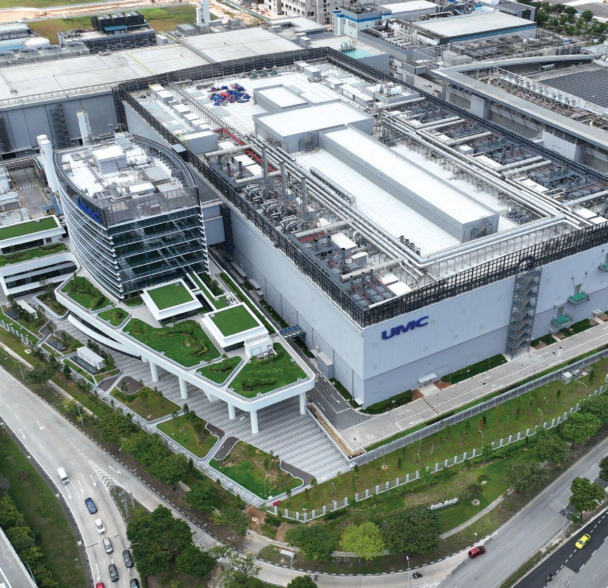
18 UMC unveils new fab expansion in Singapore
20 A*STAR’s inaugural ‘Innovate Together’ showcases Singapore’s semiconductor ambitions on global stage
President Er. Chan Ewe Jin
Chief Editor T Bhaskaran t_b_n8@yahoo.com
Publications Manager Desmond Teo desmond@iesnet.org.sg
Editorial Panel
Dr Victor Sim
Dr Chandra Segaran
Dr Ang Keng Been
Dr Aaron Sham
Mr Jaime Vega Bautista Jr
Mr Soon Ren Jun Media Representative Trevor Teh TSE@mnc-link.com
The Hi-Flo Next Generation bag filters have been developed with performance and sustainability in mind. Performance means long service life, low energy consumption and stable filtration efficiency throughout its lifetime.


Extended operating life with the best Total Cost of Ownership (TCO)
Lowest energy consumption and initial pressure drop
Reduced energy consumption
12% vs old Hi-Flo generation 30% vs industry average
Superior indoor air quality
Particle efficiency meets requirements according to the European Standard EN779 and ISO16890 for indoor air quality (IAQ)
Reduced labour cost
25-50% Longer filter lifetime, compared to synthetic bag filters
Improved air flow
Conical and tapered pocket shape allows better airflow through the filter
Optimised design for high performance Fully incinerable with the plastic frame
Using Camfil Life Cycle Cost (LCC) Analysis software, our experts conduct a comparative analysis of different air filters to provide you with a comprehensive report on potential savings.
Camfil offers a complimentary Life Cycle Cost analysis and supports you in selecting the right air filter solution.
SCAN THE QR CODE to complete the survey. Accuracy is subject to information provided.


22 Smart manufacturing in Asia: harnessing data for a resilient future
24 Vision-assisted robotics for handling delicate products with high accuracy
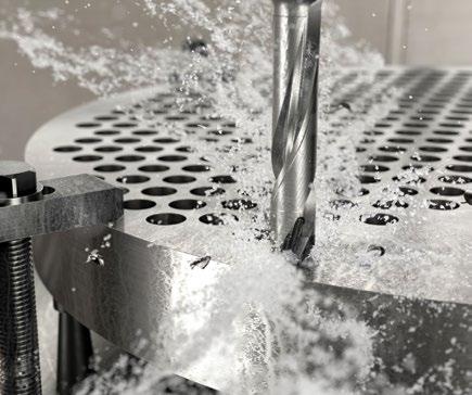
26 Mastering high-volume hole making
TESTING & CERTIFICATION
28 New heights for materials characterisation
ENGINEERING
30 6G innovation validation challenges
CYBERSECURITY
32 Nine reasons APAC businesses should prioritise privileged access management
34 Check Point’s 2025 Cloud Security Report exposes dangerous blind spots
ELECTRICAL ENGINEEERING
35 Overcoming challenges in long cable runs
SUSTAINABILITY
36 Racing towards a greener future PRODUCTS & SOLUTIONS
38 New AC-DC power supply series
39 Advanced Analogue to Digital CAN Module launched
40 Optimising laser drilling applications


The Singapore Engineer is published monthly by The Institution of Engineers, Singapore (IES). The publication is distributed free-of-charge to IES members and affiliates. Views expressed in this publication do not necessarily reflect those of the Editor or IES. All rights reserved. No part of this magazine shall be reproduced, mechanically or electronically, without the prior consent of IES. Whilst every care is taken to ensure accuracy of the content at press time, IES will not be liable for any discrepancies. Unsolicited contributions are welcome but their inclusion in the magazine is at the discretion of the Editor.
The IES Scholarship 2025 is now open for application!
If you are a Singapore citizen or PR pursuing a full-time engineering/technology-related degree, diploma, or ITE programme, this could be your chance to receive financial support for your studies.
Why apply?
4 For students passionate about engineering
4 Recognises academic excellence and co-curricular achievements
4 Priority given to those facing financial challenges
Eligibility:
• Local university undergraduates (engineering/tech degrees)
• Polytechnic diploma students (engineering/tech programmes)
• ITE students (Nitec/Higher Nitec in engineering/tech)
More information (including application form) can be found here: https://www.ies.org.sg/coresoftcloud001/ccms.r?pageid=10790&TenID=IES
Submit applications to: Scholarship@iesnet.org.sg
Deadline for submission: 25 August 2025
Don’t miss this opportunity to fuel your engineering journey!
IES President, Er. Chan Ewe Jin was invited to deliver a keynote speech at the Belt and Road Engineering Capacity Building Forum in Chengdu, Sichuan Province, China, held on 11 and 12 June 2025.
In his address, Er. Chan focused on Singapore’s strategic achievements and practical experiences in green urban development and engineering capacity building. He highlighted the five core pillars of Singapore Green Plan 2030:
1. City in Nature – expanding green spaces and restoring natural habitats.
2. Sustainable Living – reducing waste, promoting public transport,
and encouraging community-level environmental action.
3. Energy Reset – scaling up solar energy and electrifying transport.
4. Green Economy – developing a green finance and innovation hub.
5. Resilient Future – strengthening resilience of flood prevention, food security, and supply chain.
He also showcased Singapore’s key achievements in green infrastructure and cited three landmark green projects: Gardens by the Bay, Punggol Eco-Town and Tengah Forest Town.
The forum was hosted by the China Association for Science and Technology (CAST) and coorganised by the China Union of

Engineers, Tianjin University, the Sichuan Provincial Department of Science and Technology, and the Sichuan Association for Science and Technology.

Members of the IES delegation with representatives of ICE Singapore Chapter.
On the evening of 25 June 2025, an IES delegation led by President Er. Chan Ewe Jin, Emeritus President Er. Chong Kee Sen, Vice President for External Relations Dr Victor Sim, as well Chairman for Chartered Engineering Board, Mr Lew Yii Der, hosted a fruitful and extensive meeting with the representatives
from the Institution of Civil Engineers (ICE) Singapore Chapter.
ICE Singapore Chapter was represented by President Mr Robin Wilkinson, Immediate Past President Ms Sybil Tan, Singapore Country Representative Mr George Wall, and Vice President Mr Tan Zhi Howe.
There were plenty of in-depth
discussions and knowledge sharing, on many subjects including the possibility of mutual recognition of professional accreditation schemes.
Both sides are extremely glad to have reignited the discussions and taken an important step forward on future collaboration opportunities that this partnership may bring.
A UN Body responsible for setting up a carbon market under the Paris Agreement adopted important new standards to guide how emissionreducing projects measure their impact.
Known as the Paris Agreement Crediting Mechanism (PACM), it enables countries and other actors to work together on reducing greenhouse gas emissions by generating high-integrity carbon credits that support global efforts to fight climate change.
Key standards agreed
The rules adopted set out how to measure a project’s actual emission reduction impact under the mechanism.
Specifically, two key standards were agreed:
• A standard for estimating the emissions that would have happened without a project under the mechanism (known as the ‘baseline’).
The adoption of this standard is a historic step in ensuring that crediting under the mechanism reflects the ambition of the Paris Agreement.
It includes a requirement for an initial downward adjustment – for example, setting historic or current baselines at a level 10% below business-as-usual emissions – as well as a minimum 1% downward adjustment over time across all baseline approaches.
These features are designed to drive ongoing improvement and help avoid over-crediting by steadily lowering the benchmark against which emission reductions are measured.
• A standard for accounting for any unintended increases in emissions that might happen elsewhere as a result of a project (known as ‘leakage’).
The leakage standard will help
those developing methodologies to identify all potential sources of emissions. It clarifies that projectlevel REDD+ activities must be included in the host country’s national REDD+ strategy in order to qualify, helping ensure alignment with national climate efforts and reinforcing the credibility of emission reductions.
The agreed standards reflect wide input from experts and stakeholders. They are key to ensuring that carbon credits issued under the PACM are ambitious, real, additional and verifiable.
Beyond adopting the baseline and leakage standards, the Supervisory Body also made a number of related decisions to support implementation.
These include a process of consultation on how project benefits can be shared equitably with host countries, and a renewed focus on capacity building to help countries build the systems they need to take part in the mechanism – including through clearer roles for host countries.
The Supervisory Body also adopted a decision on the transition of cookstove activities, bringing earlier projects in line with the latest available data and guidance.
“This was a very significant meeting. We finally adopted a groundbreaking decision ensuring crediting levels are set consistently with a pathway to net neutrality, through a process of minimum downward adjustment of crediting levels over time,” said Martin Hession, Chair of the Supervisory Body.
“We are already uniquely placed to support host countries considering crediting, and have decided here to enhance communication with countries,
by providing a dedicated channel for them to secure their fair share of mitigation benefits, initiating a dialogue on host country roles and responsibilities, as well as exploring options for enhanced and targeted capacity building. We have also moved to ensure the quality of certain transition projects by requesting the application of the most recent applicable data,” he added.
“We are grateful for the ongoing engagement and feedback from stakeholders throughout this process, and for the Methodology Panel’s work in helping to draft these standards. They provide the clarity developers need to begin designing activities under the Paris Agreement Crediting Mechanism and are key to fully operationalising it,” said Maria AlJishi, Vice Chair of the Supervisory Body.
The outcome of this meeting paves the way for methodologies under the PACM to accelerate implementation. While this marks important progress, fewer than anticipated project transitions from the Clean Development Mechanism are expected to result in a shortterm funding gap, until a pipeline of new projects using PACM methodologies begins to build from 2026 onward.
The Supervisory Body will continue to monitor the funding situation carefully and will be reporting to the Parties to the Paris Agreement on this matter.
With the foundations in place, the Supervisory Body will continue developing other key elements of the mechanism, including additional tools, guidelines and the Mechanism Registry.
The first PACM methodologies are expected to be approved by the Supervisory Body by the end of the year.
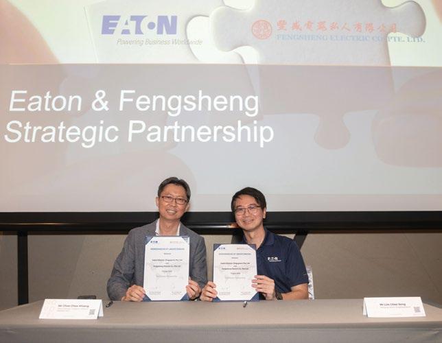
Intelligent power management company, Eaton, has appointed Fengsheng Electric as an authorised distributor for its single-phase Uninterruptible Power Supply (UPS) solutions in Singapore. This partnership strengthens Eaton’s distribution network and extends its reach into new segments across residential, commercial and industrial projects – complementing its existing strong presence in the IT segment.
“Singapore’s drive towards a smart nation and its vibrant ecosystem of SMEs and multinational corporations necessitate reliable power at every level of their critical infrastructure. Through our collaboration with Fengsheng Electric, we are enabling more businesses in Singapore to future-proof their power systems and operate with confidence, without the worry of costly downtime,” said Brian Neo, Country Manager, Singapore, Eaton’s Electrical Sector.
“We are thrilled to partner with Eaton, a recognised leader in power management solutions. We pride ourselves on being a reliable, onestop supplier of quality electrical products for industrial to residential applications,” said Lim Chee Seng, Managing Director of Fengsheng Electric.
“Eaton’s industry-leading UPS solutions are a strong addition to our existing portfolio, allowing us to offer customers even greater choice and assurance in meeting their power protection needs. With Eaton, we continue our commitment to delivering the best from the most trusted names in the industry,” he added.
As Eaton expands its channel partner network, the company is also deepening its commitment to powering the digital future, with
the launch of its next-generation 9PX Gen 2 UPS. With up to 97% efficiency, the next-gen 9PX Gen 2 (5–11 kVA) UPS helps cut operating costs.
Rising energy costs, proliferation of GPUs, and expanding IT infrastructure across Asia are fuelling a surge in demand for more efficient, reliable power protection – especially at the edge. The 5.1–10 kVA single-phase UPS market in the Asia & Oceania region is estimated at USD 100 million in 2025, with projected annual growth at 10%.
Designed as edge-ready solutions, the 9PX Gen 2 aims to help end-users as well as managed service providers meet modern business and IT power protection demands. Key features include:
• High performance and energy efficiency: Up to 97% efficiency in online mode.
• High power density in a compact footprint, freeing up valuable rack space for other critical equipment.
• Enhanced user experience, compatibility and connectivity features including Advanced Battery Management (ABM+) that increases battery service life by up to 50% through predictive maintenance.
• Versatile deployment: Ideal for small data centres, enterprise data rooms, mission-critical applications across healthcare, light industrial and education, and more.
“We are committed to meeting the growing need for robust and efficient power management, particularly in the rapidly expanding edge computing and small data centre landscapes across Asia,” said Choo Chee Khiang, General Manager, Singapore, Indonesia & Malaysia, Eaton’s Electrical Sector.
“Built on a trusted legacy of excellence, the enhanced 9PX Gen 2 delivers improved performance and efficiency, ensuring peace of mind for always-on, uninterrupted operations,” he added.
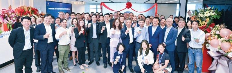
GigaDevice, a leading semiconductor company specialising in Flash memory, 32-bit microcontrollers (MCUs), sensors and analog products, officially opened its global headquarters in Singapore, recently.
This strategic move marks a major milestone in GigaDevice’s international growth journey, underscoring its commitment to closer customer engagement, building a resilient and agile supply chain, and strengthening its ecosystem and brand presence across key global markets.
GigaDevice has, over the years, built a competitive product portfolio and innovative solutions. Its SPI NOR Flash commands the No 2 global position with a 20.4% market share, and it ranks No 7 worldwide in the 32-bit generalpurpose MCU segment.
Serving diverse sectors including industrial, automotive, consumer and IoT, GigaDevice is recognised for delivering semiconductor solutions with reliability and innovation at its core. As global demand for smart, connected technologies accelerates – particularly in industrial automation, automotive electronics and intelligent edge devices –GigaDevice is sharpening its focus on innovation, supply chain agility and ecosystem collaboration.
The company is positioning itself to meet the evolving needs of international customers and capture opportunities across fastgrowing markets.
“We chose Singapore not just for its strategic location, but for its clarity, consistency and global ambition. This is more than a regional office – it is a collaborative innovation hub where expertise across disciplines and borders comes together to build smarter systems, accelerate execution and power what is next,” said Jennifer Zhao, GigaDevice Global Business CEO.
Singapore’s robust infrastructure, pro-innovation environment and exceptional talent pool have established it as a global premier technology and business hub. Its strong connectivity, transparent regulatory framework, and dedication to digital transformation provide the ideal foundation for companies like GigaDevice to scale globally while maintaining agility and future readiness.
Functioning alongside GigaDevice’s group headquarters in China, the Singapore global headquarters will serve as a central platform to drive global coordination, foster localised product innovation, and deepen collaboration with customers and supply chain partners. From
this base, the company aims to expand its presence in international markets and build a more connected, agile and responsive global ecosystem.
GigaDevice
GigaDevice Semiconductor Inc is a leading, global, fabless supplier. The company was founded in April 2005 and is headquartered in Beijing, China, with branch offices in many countries and regions worldwide, providing local support to customers.
Committed to building a complete ecosystem with four major product lines – Flash memory, MCU, sensor and analog – as the core driving force, GigaDevice can provide a wide range of solutions and services in the fields of industrial, automotive, computing, consumer electronics, IoT, mobile, networking and communications.
GigaDevice has received the ISO26262:2018 automotive functional safety ASIL D certification, IEC 61508 functional safety production certification, as well as ISO9001, ISO14001, ISO45001, and Duns certifications.
GigaDevice has also formed strategic alliances with leading foundries, assembly and test plants, to streamline supply chain management.
81 Electrical, an electrical service provider in Singapore, has announced the launch of its control panel automation services.
The new services are designed to bring advanced automation, remote monitoring, and energyefficient solutions to industries, such as ACMV, water treatment, building management, and more. As industries continue to evolve, the demand for smart, automated systems is on the rise. Recognising the inefficiencies of traditional manual control panels, 81 Electrical has developed an automation solution that incorporates PLC programming, HMI integration, and cloud-based remote monitoring. These innovations result in increased operational efficiency, reduced downtime and significant cost savings. In this way, industry needs are addressed.
“Outdated control systems are holding businesses back. Our new automation services provide a smarter, more sustainable alternative that empowers clients with real-time control and insights,” said Steven Koh, Director of 81 Electrical.

Important features of the new services include remote monitoring and control, provision of realtime alerts via SMS and email; integration with existing ACMV, pump, and building management systems; and energy-efficient design to lower operating costs. The launch also marks the beginning of a broader expansion. Upcoming services include smart home and building automation; advanced electrical control
panel solutions; swimming pool automation; remote monitoring & system control; industrial automation (PLC, HMI, SCADA); and pump & motor repair and servicing.
81 Electrical also aims to help clients lower their carbon footprint and extend the lifespan of their systems, by optimising energy consumption, enabling predictive maintenance and reducing the risk of equipment failure.
Eaton and Siemens Energy, a leading energy technology company, have announced a fast-track approach to building data centres with integrated onsite power. They will address urgent market needs by offering reliable grid-independent energy supplies and standardised modular systems to facilitate swift data centre construction and deployment. The collaboration will enable simultaneous construction of data centres and associated onsite power generation with grid connection and the integration of renewables to meet regional regulatory requirements.
Siemens Energy’s modular and scalable power plant concept is tailored to the specific needs of data centre operators. The standard configuration generates 500 megawatts (MW) of electricity, featuring highly efficient SGT-800 gas turbines, redundancy and additional battery storage systems, ensuring the highest reliability.
The plant can be scaled up and down. In the future, it can also operate in a carbon-neutral manner, provided hydrogen is available as part of the data centre’s sustainability strategy. The Siemens Energy concept also
includes an optional emission-free clean air grid connection, to be installed either during construction or as a retrofit, enabling data centres to provide grid services.
Eaton will provide customers with electrical equipment such as medium voltage switchgear, low voltage switchgear, UPS, busways, structural support, racks and containment systems, engineering services and the software offerings needed to protect and enable IT loads from the medium-voltage grid to the chip, and help to build and commission data centres with skidded and modular designs.
A pioneering collaboration between ACwise and Ngee Ann Polytechnic’s Centre for Environmental Sustainability (CfES) is demonstrating how certified energy-saving technologies can cut costs while reducing scope 2 and 3 emissions, offering a practical path towards sustainable operations.
Through this partnership, building owners have collectively saved SGD 1.2 million in energy costs in recent months, by integrating ACwise’s NanoRefrigerant into HVAC systems. This innovative solution improves efficiency, reduces emissions and extends equipment lifespan, offering a practical, costeffective path to greener buildings. Real-world results highlight the impact of this collaboration.
Seo Eng Joo Food Hub, which manages several large cold storage facilities across Southeast Asia, was able to reduce its HVAC-R energy consumption by 19%.
Song Fish, a leading frozen seafood and poultry supplier, achieved a 12.3% reduction in HVAC energy consumption through a recent trial.
At the core of this success is the academic-industry collaboration.
By combining CfES’s rigorous research with ACwise’s industry expertise, the initiative accelerates the adoption of proven, highperformance solutions. The Singapore Green Building Council (SGBC) certification further reinforces the credibility of these technologies, ensuring they meet stringent sustainability standards.
“Our collaboration goes beyond technology. We are creating a replicable framework that demonstrates how academic insights can drive meaningful industry transformation. Each percentage point of energy saved represents not just financial benefit, but a step towards Singapore’s net zero target by 2050,” said Tommy Chan, Founder and CEO of ACwise.
“CfES is committed to bridging innovative research with real-world applications, and our collaboration with ACwise exemplifies this approach. By rigorously assessing the performance of NanoRefrigerant in a VRF air-
conditioning system, the results have demonstrated measurable efficiency gains, reinforcing the importance of evidence-based solutions in advancing sustainability within the built environment,” said Jason Tang, Chief Sustainability Officer, Ngee Ann Polytechnic and Director, CfES.
The initiative’s impact extends beyond immediate savings.
Building owners are not just cutting costs. They are channelling savings into sustainability upgrades like solar panels and smart energy systems. These investments go beyond individual buildings, strengthening Singapore’s green ecosystem and driving continuous improvements in energy efficiency.
CfES has played a key role in translating and developing technologies and solutions into practical innovations for industry. The centre has successfully completed over 500 consultancy and R&D projects, filed more than 30 patents and know-hows, and licensed 1 in 3 of its intellectual properties.
Sembcorp Industries (Sembcorp) and Aster Chemicals and Energy (Aster) have announced new energy and utilities partnerships in Southeast Asia.
As part of the collaboration, Sembcorp will provide a comprehensive suite of gas, power and utilities solutions, with a total contract value of over SGD 650 million, to Aster which operates an integrated refining and chemical complex in Pulau Bukom and Jurong Island.
In addition to the commercial agreements, Sembcorp and Aster also signed a Memorandum of Understanding (MoU), valid for six

months from its date of execution, to explore strategic initiatives across Singapore, Indonesia and the rest of Southeast Asia.
This includes collaborating on cogeneration and utilities projects
for Aster, regional gas procurement, joint infrastructure investments, and establishing industrial parks in Indonesia – aligning with their shared vision for sustainable growth and addressing rising energy demands.
Siemens Digital Industries Software recently announced that it is making its AI-enhanced electronic systems design technology more accessible to small and midsized businesses, with PADS Pro Essentials software and Xpedition Standard software.
Built on Siemens’ Xpedition technology, these new offerings combine intuitive user experiences, integrated cloud collaboration and AI-driven automation to empower small teams and independent engineers, with the same professional-grade capabilities trusted by the world’s most advanced electronics companies, at a fraction of the cost.
“Today’s launch marks a major milestone in our strategy to democratise access to highperformance PCB design and bring the transformative power of AI to the PCB design workflow. With PADS Pro Essentials and Xpedition Standard, we are delivering scalable solutions that help smaller teams move faster, work smarter and design with confidence, without sacrificing quality or budget,” said AJ Incorvaia, Senior Vice President, Siemens EDA.
PADS Pro Essentials delivers a streamlined, cloud-connected design environment, built on Siemens’ proven Xpedition technology at an entry-level price. Tailored for independent engineers and startups, it includes schematic capture, layout and a seamless design experience that lowers barriers to professional-grade PCB design tools. The Essentials tier also introduces an integrated, co-branded front-end powered by CELUS, allowing engineers to design using intelligent functional blocks with AI-assisted schematic and BOM generation.
Xpedition Standard is built for
Siemens’ Xpedition Standard is built for teams that need a balance of cost-efficiency and advanced capabilities such as design reuse, variant management, advanced routing automation, native 3D layout and deep collaboration.
growing teams that need a balance of cost-efficiency and advanced capabilities. It adds powerful features like design reuse, variant management, advanced routing automation, native 3D layout and deeper collaboration across mechanical, manufacturing and supply chain stakeholders.
Teams can further extend capabilities using token-based options, which provide ondemand access to more advanced capabilities such as fully integrated pre- and post-layout signal integrity analysis powered by Siemens’ Hyperlynx software for PCB analysis and rigid-flex design, without requiring a full tier upgrade.
“We took a close look at Xpedition Standard and were genuinely impressed. Siemens has clearly reimagined the experience. It is intuitive, modern, and far more connected and integrated than we expected. From day one, it felt like a tool built for the way we actually work. I can get real design work done without fighting
the software,” said Shrouk ElAttar, Founder, Shrouk El-Attar Consultancy.
Part of the Siemens Xcelerator portfolio of industry software, both new offerings are part of the Xpedition family and are designed to grow with engineers, from individual users to global enterprises. The unified user experience, design libraries and cloud-based collaboration infrastructure provide a seamless upgrade path as team and project requirements evolve.
Siemens Digital Industries
Siemens Digital Industries software helps organisations of all sizes digitally transform using software, hardware and services, from the Siemens Xcelerator business platform. Siemens’ software and the comprehensive digital twin enable companies to optimise their design, engineering and manufacturing processes, to turn today’s ideas into the sustainable products of the future – from chips to entire systems, from product to process, across all industries.
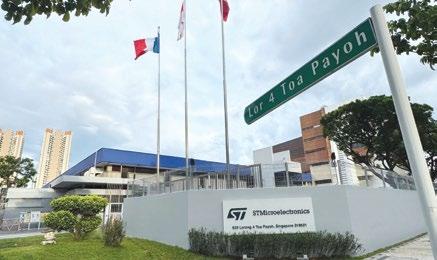
STMicroelectronics (ST), a global semiconductor leader serving customers across the spectrum of electronics applications, has appointed Singapore Power (SP Group) to upgrade the cooling infrastructure at ST’s Toa Payoh site which serves as a critical hub for its packaging R&D and wafer testing operations. This new system will improve energy efficiency and aims to reduce carbon emissions by approximately 2,140 tons annually.
“Following the landmark agreement with SP Group, in 2022, to implement Singapore’s largest industrial district cooling system at our operations in AMK TechnoPark, the upgrade to the cooling system in our Toa Payoh site demonstrates ST’s continued commitment to innovative cooling solutions and to become carbon neutral by 2027,” said Jean-Louis Champseix, Group VP, Head of Sustainability, at STMicroelectronics.
“With cooling accounting for a large proportion of our site’s overall energy consumption, the improved efficiency of this new system will further reduce our carbon footprint while ensuring we meet Singapore’s MEES regulations.” he added.
“This project underscores how strategic partnerships and smart infrastructure can accelerate decarbonisation in energy-intensive industries like manufacturing. Together with ST, we have developed a tailored, integrated cooling solution that strengthens operational resilience and sustainability,” said S Harsha, Managing Director for Sustainable Energy Solutions (Singapore), SP Group.
“This partnership reflects our commitment to engineering a more sustainable future for our customers and the built environment, and we look forward to expanding similar solutions
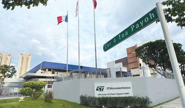
across the region,” he added.
With a cooling capacity of up to 3,200 refrigerant tons (RT), the new cooling system’s dual-temperature capability supplies both low and medium temperature cooling directly, eliminating the need for heat exchangers currently used to produce medium temperature cooling. It is designed to support all facility needs, saving up to five Gigawatt-hours of energy annually.
Under the agreement, SP Group will design, build, operate and maintain the new chiller cooling system, providing chilled-wateras-a-service under a 20-year contract. The construction and implementation phases are expected to be completed by December 2025.
The upgrade aligns with the National Environment Agency’s (NEA) Minimum Energy Efficiency Standards (MEES), which comes into effect in December 2025, and is aligned with the strong sustainability agenda of the Singapore government, particularly the SG Green Plan 2030. By
embracing these initiatives, ST Singapore not only contributes to global environmental goals but also supports Singapore’s vision of a sustainable future.
STMicroelectronics
As an integrated device manufacturer, STMicroelectronics works with more than 200,000 customers and thousands of partners to design and build products, solutions and ecosystems, that address their challenges and opportunities, and the need to support a more sustainable world.
SP Group
SP Group is a leading utilities group in the Asia Pacific, empowering the future of energy with lowcarbon, smart energy solutions for its customers. About 1.7 million customers benefit from SP Group’s transmission, distribution and market support services.
SP Group also provides sustainable and renewable energy solutions for local and regional customers.

HANNOVER MESSE 2025 was held, from 31 March to 4 April 2025, in Hannover, Germany.
The event, considered to be the world’s leading industrial trade fair, featured the products and technologies of 4,000 exhibiting companies, attracting around 127,000 visitors from 150 countries. More than 40% of the visitors came from outside Germany.
The main exhibition areas were Smart Manufacturing, Digital Ecosystems, Energy for Industry, Compressed Air & Vacuum Technology, Engineered Parts & Solutions, Future Hub, and International Trade & Investment. A conference programme with about 1,600 speakers complemented the exhibition.
“HANNOVER MESSE 2025 was a powerful commitment to the future viability of industry in Germany and Europe – in close cooperation with its international partners,” said Dr Jochen Köckler, CEO of Deutsche Messe AG, organisers of the event.
Dr Gunther Kegel, President of the German Electrical and Electronic Manufacturers’ Association (ZVEI) and Chairman of the HANNOVER MESSE Exhibitors’ Advisory Board, said, “HANNOVER MESSE has once again shown that it is the most important platform for industrial innovation.
AI in industrial applications was of particular interest to visitors, especially those from abroad.”
Thilo Brodtmann, Managing Director of the German Mechanical Engineering Industry Association (VDMA), said, “This year’s HANNOVER MESSE has shown, in particular, how important good partnerships and open markets are for an export and innovation-driven industry such as machine building and plant engineering.”
AI: number one topic in industry
The number one topic at this year's trade fair concerned AI applications for industry.
“AI has the potential to change industry more in just a few years than it has changed in the entire past decade. The exhibiting companies used specific examples to show how manufacturing companies can benefit from artificial intelligence. Through the targeted use of these technologies, small and mediumsized enterprises can also increase their efficiency, reduce costs, and significantly increase their competitiveness,” said Dr Köckler.
A new study presented at HANNOVER MESSE by the VDMA and the consulting firm Strategy& shows this in concrete terms. According to the study, the use of
generative artificial intelligence can increase the profit margin in mechanical and plant engineering by up to 10.7 percentage points.
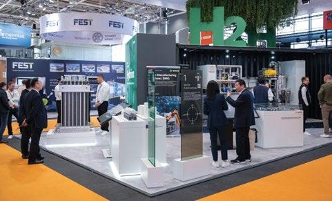
Hydrogen for a sustainable energy supply
In the energy halls at HANNOVER MESSE, everything revolved around efficiency and sustainability. Hydrogen played a prominent role in this. In Hall 13 alone, around 300 companies presented their latest developments and applications in the field of hydrogen and fuel cells at the ‘Hydrogen + Fuel Cells EUROPE’ stands.
Partner Country
Partner Country Canada presented itself impressively at HANNOVER MESSE. The innovative role of Canadian companies and institutions in key areas such as artificial intelligence, digitalisation and renewable energies is particularly noteworthy. The close cooperation with international partners and the strong focus on sustainable technologies underline Canada's importance as a dynamic player in the global markets of the future.
The next edition of the event will be held in Hannover, from 20 to 24 April 2026. Brazil is the Partner Country.
Industrial component cleaning is facing a variety of challenges. Specifications call for stricter cleanliness for parts and components, and there are greater demands for cost-effective cleaning, and more exacting requirements for energy and resource efficiency in processes.
Organised by Deutsche Messe AG, parts2clean 2025, the 21st leading international trade fair for industrial parts and surface cleaning, will present a comprehensive range of industrial cleaning solutions for reconciling these, sometimes, contradictory objectives.
The event will be held from October 7 to 9, 2025 at the Stuttgart Exhibition Center in Germany.
Components and assemblies are becoming increasingly compact, complex, and sensitive to contamination, in almost all sectors, including new mobility, electronics, the semiconductor industry, sensor technology, optics, medical technology, the pharmaceutical industry, aerospace, and defence.
This is resulting in more stringent cleanliness requirements for component cleaning.
Accordingly, adapted or optimised cleaning processes are required. In parallel to this, the cleanliness of the production environment is becoming increasingly important, in order to minimise contamination and to avoid cross-contamination and recontamination. These aspects
also play a key role when it comes to the cost-effectiveness of cleaning. In addition, husbanding of resources and a reduced carbon footprint are also becoming increasingly vital core requirements in component cleaning.
Cleaning solutions that are in demand
“With the most up-to-date and comprehensive international offering in the field of industrial cleaning technology, parts2clean will present solutions that can effectively meet the increased demands on component cleaning, from a technological, economic, and ecological point of view,” said Ramtin Randjbar-Moshtaghin, Project Director at Deutsche Messe AG.
The exhibitors’ solution portfolio is optimally adapted to the respective production step, the component geometry, and material, as well as to the contamination and cleanliness requirements – from deburring and pre- or intermediate cleaning to final and high-purity cleaning. Topics such as automation, digitalisation, and artificial intelligence (AI) also play a role.
“The complete and innovative range of exhibits makes parts2clean the world’s most important information and procurement platform for industrial cleaning technology. This is also indicated by the fact that the leading international trade fair attracts almost exclusively trade visitors
(99%), about 80% of whom come with intent to invest,” added Ramtin Randjbar-Moshtaghin.
Supporting programme and award ceremony
The supporting programme will also enable transfer of knowledge on trends, innovations and benchmark applications, that are in demand worldwide.
The exhibitors’ cleaning solutions crossing industry, technology and material disciplines will be complemented by an attractive supporting programme.
This includes the bilingual p2c.EXPERTFORUM, which has established itself as a highly prized source of knowledge.
It will be organised and held in cooperation with the Fraunhofer Cleaning division and the German Industrial Parts Cleaning Association (FiT).
“The topics of the simultaneously translated (German to English and English to German) presentations will provide information about current challenges, new developments and trends in industrial parts cleaning as well as benchmark applications and basic knowledge,” said Ramtin Randjbar-Moshtaghin.
A highlight of the supporting programme at this year’s event will be the presentation of the 4th FiT2clean award. The annual award honours outstanding achievements and innovative solutions in industrial parts cleaning.

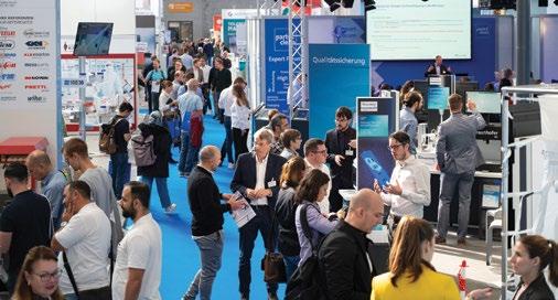
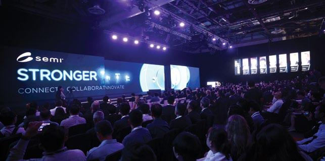
SEMICON Southeast Asia 2025, the region’s flagship global electronics manufacturing and semiconductor supply chain event, concluded with over 25,000 attendees, including global CEOs, C-suite executives, leaders, decision-makers, summit delegates, exhibitors, and speakers, converging on Singapore for the 30th edition of the region’s most prominent microelectronics event.
SEMICON Southeast Asia 2025, held from 20 to 22 May at the Sands Expo and Convention Centre, Marina Bay Sands, Singapore, exceeded expectations, underscoring Southeast Asia’s growing influence in the global semiconductor ecosystem.
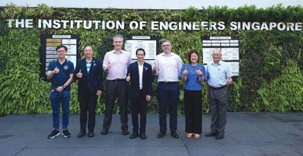
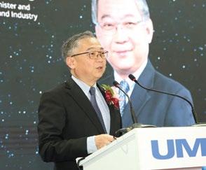
The event officially opened on 20 May with a ceremony graced by Guest-of-Honour, Dr Tan See Leng, Second Minister for Trade and Industry, and Minister for Manpower.
The three-day event was praised for its scale, calibre of participants, and multifaceted programmes, making it not only a celebratory occasion but also a definitive platform for innovation, collaboration and industry advancement, to overcome business challenges and headwinds.
A MULTI-FACETED SHOWCASE
SEMICON Southeast Asia 2025 presented a wide-ranging and immersive experience for industry stakeholders, spotlighting highimpact programmes, cuttingedge innovations and strategic engagements, across all facets of the microelectronics value chain. This year’s edition drew a record number of engagements from regional and international participants, reinforcing Southeast Asia’s rising prominence in the global semiconductor landscape.
Industry Keynote
Delivered by Dr Tien Wu,


Attendees at the Opening Ceremony.
Chief Executive Officer of ASE, the Keynote titled ‘Redefining the Collective Value of the Semiconductor Industry’, set the tone for the event by exploring the broader purpose and collaborative future of the semiconductor industry.
The inaugural CEO Summit, moderated by CNBC correspondent and anchor, Ms Chery Kang, was a headline event that drew a full-capacity audience of senior executives, business leaders, and decision-makers.
It featured thought-provoking sessions led by top global semiconductor leaders – including the CEOs and Presidents of Applied Materials, GlobalFoundries, Infineon Technologies, Sandisk, and Soitec.
Topics ranged from navigating global supply chain complexities

and scaling AI-driven manufacturing to ensuring long-term sustainability and talent resilience. The summit provided rare access to C-suite perspectives shaping the industry’s strategic direction.
A cornerstone of the event was its strong emphasis on talent development, featuring a suite of programmes, designed to attract
and upskill the next generation of semiconductor professionals, such as SEMI TECH Zoomer University Bootcamp, Career Exploration Fair, TalentCONNECT, and Semiconductor Regional HR Forum.
Sustainability in Focus
SEMICON Southeast Asia
2025 underscored its growing commitment to sustainability through the Global Climate Summit (GCS) Workshops, co-hosted by SEMI and its hyperscaler partners. These workshops delivered actionable tools for carbon reduction, shared best practices in emissions tracking, and introduced collaborative frameworks to advance measurable environmental progress across the semiconductor supply chain.
Exclusive Business Matching & Networking
Strategic networking opportunities were a key feature of the show, helping to foster cross-border partnerships and commercial opportunities such as the Star Buyers Programme and handshake@SEMICON.
Innovation Showcases & Pavilions
Across three levels of the Sands Expo and Convention Centre, the exhibition floor featured over 1,400 booths representing more than 700 companies. The showcases spanned every segment of the semiconductor ecosystem, including the IC Design Pavilion, dedicated to next-generation chip architecture and integrated circuit innovation, and other exhibitions showcasing advanced packaging, smart manufacturing, AI integration, MEMS, materials innovation, and factory automation solutions.
International Presence and Strategic Alliances
This milestone edition featured 10 global and government pavilions, representing China, the European Union, Japan, Malaysia, Poland, Singapore, South Korea, Taiwan,
the Netherlands, and Vietnam.
SEMICON Southeast Asia 2025 also welcomed numerous foreign dignitaries and highlevel delegations, underscoring the region’s rising influence in global semiconductor policy and investment. In addition, the event served as a strategic platform for international collaboration, playing host to the signing of multiple Memoranda of Understanding (MoUs) between industry players and government agencies, to advance collaborations and R&D programmes.
Honouring Industry Excellence
Held on the opening night of SEMICON Southeast Asia 2025, the Night of Leaders, Dinner and Awards ceremony paid tribute to outstanding individuals shaping the region’s semiconductor future.
Marking the event’s 30th anniversary, awards were presented across four categories –Lifetime Achievement, Industry Leader of the Year, Emerging Young Leader, and Industry Tribute Award – recognising visionary leadership, enduring contributions, and rising talent driving Southeast Asia’s semiconductor growth.
Among the evening’s distinguished awardees, Ms Mary Puma, Chair of the SEMI International Board of Directors received the SEMI Lifetime Achievement Award in recognition of her long-standing leadership in the semiconductor industry.
Mr Chen Kok Sing, Senior Vice President, Global Assembly and Test at Micron Technology, was conferred the SEMI Southeast Asia Industry Leader of the Year Award 2025, honouring his distinct role in advancing semiconductor excellence and innovation.
The scale and diversity of this year’s edition reflect the vibrancy and strategic depth of the global semiconductor value chain, as well as SEMICON Southeast Asia’s continued role as a key enabler of growth, collaboration and technology leadership in the region.
“As the semiconductor industry stands at the crossroads of unprecedented global developments and mounting uncertainty, SEMICON Southeast Asia 2025 serves as a strategic platform to forge stronger global alliances,” said Ajit Manocha, President and CEO of SEMI.
“This 30th milestone edition reflects not only the region’s rise as a key hub for innovation, talent, and manufacturing, but also the industry’s shared commitment to build a more sustainable, secure, and resilient future,” he added.
“It has been an extraordinary honour to host this landmark 30th edition in Singapore. Keeping true to this year’s theme of ‘Stronger Together’, the strong turnout and meaningful engagement reaffirm the show’s impactful role in uniting the global semiconductor ecosystem to drive collective growth and resilience,” said Linda Tan, President of SEMI Southeast Asia.
SEMICON Southeast Asia 2026, the next edition of the event, will take place from 5 to 7 May 2026, at the Malaysia International Trade and Exhibition Centre (MITEC) in Kuala Lumpur, Malaysia.
SEMI is the global industry association connecting over 3,000 member companies and 1.5 million professionals worldwide across the semiconductor and electronics design and manufacturing supply chain.
SEMI accelerates member collaboration on solutions to top industry challenges through Advocacy, Workforce Development, Sustainability, Supply Chain Management and other programmes.
SEMI’s SEMICON expositions and events, technology communities, standards and market intelligence help advance its members’ business growth and innovations.
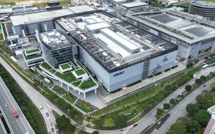
New 22 nm fab to be one of the most advanced semiconductor manufacturing facilities in the country.
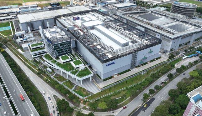
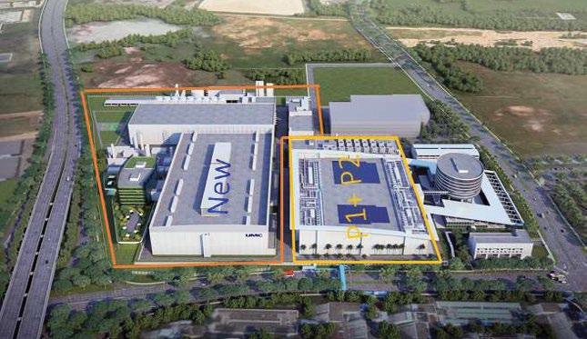
On 1 April 2025, United Microelectronics Corporation (UMC), a leading global semiconductor foundry, officially unveiled its new fab facility in Singapore, with a grand opening ceremony.
The first phase of the new facility will start volume production in 2026, bringing UMC’s total production capacity in Singapore to more than 1 million wafers annually. It will also be one of the most advanced semiconductor foundries in Singapore, manufacturing semiconductors to enable communications, Internet of Things (IoT), automotive and AI innovations.
The ceremony was graced by Deputy Prime Minister and Minister for Trade and Industry of Singapore, Mr Gan Kim Yong, the Guest-of-Honour; Senior Minister and Coordinating Minister for National Security of Singapore, Mr Teo Chee Hean; Permanent Secretary of Singapore’s Ministry of Trade and Industry, Dr Beh Swan Gin; Managing Director of the Singapore Economic Development Board (EDB), Mr Jermaine Loy; and JTC Assistant Chief Executive Officer, Ms Christine Wong.
The facility, a greenfield expansion adjacent to UMC’s existing fab in the Pasir Ris Wafer Fab Park, comprises two phases. Up to USD 5 billion will be invested to bring the first phase to full capacity of 30,000 wafers per month, with room for further investment in a second phase expansion, in the future.
The new facility is equipped for manufacturing with UMC’s industry-leading 22 nm and 28 nm solutions – the most advanced foundry processes currently in Singapore’s semiconductor sector – for global customers’ products including premium smartphone display chips, power-efficient
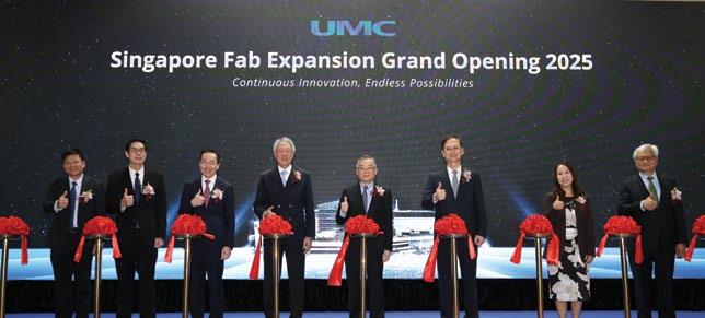
VIPs
memory chips for IoT devices, and next-generation connectivity chips.
The expansion is expected to create approximately 700 jobs locally, over the next few years, including process and equipment engineers as well as research and development engineers.
“This new state-of-the-art facility in Singapore signals a new phase of growth for UMC. It enhances our ability to meet future chip demand, driven by continuous innovations in connectivity, automotive and AI,” said Mr S C Chien, President of UMC.
“The unique geography of Singapore also makes the new facility well placed to support our
customers in strengthening supply chain resilience. This fab expansion closely aligns with the Singapore government’s vision to become a
leading advanced manufacturing hub, and we are deeply grateful for their support,” he added.
“We welcome UMC’s expansion in Singapore. This new fab introduces new leading edge specialty semiconductor capabilities and production capacity that will enhance Singapore’s competitiveness as a critical node in the global semiconductor supply chain. This significant investment underscores our long-standing partnership with UMC, and we look forward to deepening our collaboration to strengthen Singapore’s semiconductor ecosystem,” said Mr Jermaine Loy, Managing Director of the Singapore Economic Development Board.
The new facility was built according to rigorous sustainability standards, and has obtained the Green Mark GoldPLUS certification from Singapore’s Building and Construction Authority. In alignment with UMC’s goal to be 100% powered by renewable energy, by 2050, the new facility will has solar panels installed on its rooftop, over an area of 17,949 m2.
In addition to the manufacturing site, the expansion also includes a brand-new office building, a fullsized multipurpose sports hall, and other amenities for employees and community members.
United Microelectronics Corporation (UMC) is a leading global semiconductor foundry company, providing wafer fabrication services to more than 400 customers worldwide, in all sectors of the electronics industry.
UMC operates 12 fabs across Taiwan, Singapore, China and Japan, with a total production capacity of 5 million wafers annually.
UMC is among the world’s top pure-play foundries –semiconductor manufacturers that produce IC wafers for customers, based on their designs. The company’s comprehensive portfolio of process technologies is used to produce a wide range of
chips critical for enabling wireless communications, Internet of Things (IoT), automotive, and artificial intelligence (AI).
Founded in 1980 as Taiwan’s first semiconductor company, UMC is headquartered in Hsinchu and has a total of 20,000 employees worldwide. The company has offices in the US, Europe, China, Japan, Korea and Singapore.
In 2000, UMC established the first 12-inch (300-millimetre) fab in Singapore’s Pasir Ris Wafer Fab Park. With an annual capacity
of 678,000 wafers (2024 figures), UMC Singapore accounts for nearly 14% of the company’s total production capacity. Singapore is also a significant research and development hub for UMC, with the company’s largest R&D team outside of Taiwan.
Products manufactured at UMC Singapore include display driver and wireless connectivity chips for smartphones, microcontroller unit chips for car control systems, and silicon interposers for AI graphic processing units (GPUs) in data centres.
2000 Established as Singapore’s first 12-inch fab, through a joint venture
2005 Became a wholly owned UMC subsidiary
2013 Designated UMC’s Center of Excellence to spearhead specialty technology R&D
2018 Received the Watermark Award, Singapore’s top honour for water conservation
Certified to IATF 16949 standard for automotive quality management
2022 Groundbreaking of new greenfield fab
2024 Received the Water Efficiency Awards Moved first tool into new fab
2025 Grand opening of new fab, readying for 2026 volume production
Milestones in UMC’s growth in Singapore.
New initiatives and global partnerships were unveiled during the inaugural event to strengthen Singapore’s semiconductor capabilities.
The Agency for Science, Technology and Research (A*STAR) hosted the inaugural ‘Innovate Together’ event at SEMICON Southeast Asia 2025, signalling Singapore’s bold ambition to lead in the next phase of semiconductor innovation.
Designed as a convergence point for industry, academia and the public sector, Innovate Together unveiled game-changing initiatives, strategic global partnerships and new research platforms, that will strengthen Singapore’s position as a high-value semiconductor R&D and talent hub.
“Singapore’s semiconductor ecosystem is built on strong collaborations between public agencies, academia and industry partners. The Innovate Together event exemplifies our commitment to fostering these partnerships and accelerating innovation to address industry challenges and capture new opportunities in the global semiconductor landscape,” said Professor Yeo Yee Chia, Deputy Chief Executive (Innovation & Enterprise) at A*STAR.
At the heart of Innovate Together was the launch of the world’s first industry-grade 200 mm Silicon Carbide Open R&D Line by the A*STAR Institute of Microelectronics (A*STAR IME).
In addition, A*STAR unveiled two other initiatives that will strengthen Singapore’s semiconductor research and innovation capabilities – the launch of Lab-in-Fab phase two and the launch of the EDA Garage.
LAUNCH OF 200 MM SILICON CARBIDE OPEN R&D LINE
This pioneering facility will enable and accelerate Silicon Carbide (SiC)
innovation, from materials growth and defect analysis to device fabrication and testing.
The Open R&D Line addresses key challenges faced in the development of SiC devices, including the high cost of industry-grade tools, limited access to advanced technologies, complex and fragmented development processes, and lack of collaboration and knowledge sharing.
How the industry can benefit
By offering a complete suite of SiC development and pilot manufacturing capabilities under one roof, the Open R&D Line increases the speed of R&D, by eliminating the fragmented R&D processes that previously required researchers and companies to work with multiple facilities.
The Open R&D Line enables the development of advanced technologies, by having a close partnership with key equipment OEMs and materials suppliers –ASM, centrotherm, Nissin, Soitec and Toray – who have contributed their latest technologies and are co-developing their nextgeneration products with A*STAR:
• ASM’s PE1O8 tool for depositing high-quality SiC epitaxial layers.
• centrotherm’s c.ACTIVATOR 200 and c.OXIDATOR 200 tools for hightemperature SiC annealing and oxidation.
• Nissin’s first and only in-situ X-ray diffraction capability for the SiC ion implantation process.
• Soitec’s SmartSiCTM semiconductor engineered substrate technology.
• Toray’s innovative materials
for SiC power module packaging products.
While it was being established, the Open R&D Line already demonstrated its value to the semiconductor industry. Several global and local companies have partnered with A*STAR IME to utilise its capabilities, highlighting strong industry demand for such collaborative platforms:
• STMicroelectronics is leveraging engineering capabilities and tools to develop ways to streamline its manufacturing processes and improve the quality of its SiC devices.
• One of the top foundries in the world is developing key process technologies through the Open R&D Line, with the intention to scale up production of advanced SiC devices.
• WaferLead, a local start-up, is using the Open R&D Line to develop, evaluate and enhance the performance and reliability of its wafers.
LAUNCH OF LAB-IN-FAB PHASE TWO
A*STAR Institute of Microelectronics (A*STAR IME), STMicroelectronics and ULVAC have announced phase two of their Lab-in-Fab initiative, a 200 mm R&D and manufacturing line in Singapore that is focused on piezoelectric Micro-ElectroMechanical Systems (piezoMEMS) technology.
This collaboration combines STMicroelectronics’ expertise in piezoMEMS R&D and wafer manufacturing, ULVAC’s advanced manufacturing equipment, and A*STAR IME’s expertise in piezoelectric thin film materials and
device design.
Lab-in-Fab is positioned to become a catalyst for innovation, bringing together a diverse ecosystem of sensor and actuator design companies, product companies as well as manufacturing companies and their suppliers, to collaboratively prototype and manufacture new products for various applications.
To-date, it has commercialised new lead-free piezoelectric materials and device platforms, as well as created employment opportunities in Singapore. Additionally, Institutes of Higher Learning from Singapore and globally have tapped on Lab-inFab for their research and training needs.
The second phase of Lab-in-Fab expands the partnership to include A*STAR Institute of Materials Research and Engineering and the National University of Singapore, to further accelerate the development of new piezoelectric materials and devices.
It also adds sustainability as a central focus, to develop more energy-efficient lead-free piezoMEMS transducers using environmentally friendly materials like scandium-doped aluminium nitride (ScAlN).
Outcomes of Lab-in-Fab Phase One
Lab-in-Fab phase two builds on the success of the first phase, which led to a fully operational R&D and manufacturing line for piezoMEMS transducers. A key achievement of phase one was the development of a piezoMEMS transducer platform using physical vapour deposited lead zirconate titanate (PVD PZT) thin film.
This is easier to manufacture compared to the conventional solgel method of depositing PZT thin films and reduces lead content by 99% versus traditional ceramic PZT transducers – making it a more environmentally friendly option. The platform has been offered to multiple customers for applications in medical, VR and robotics. Beyond technology development, Lab-in-Fab phase one introduced
a Multi-Wafer Project (MPW) service for local and international universities and institutes, enabling new innovations for piezoMEMS devices and applications. This service will continue to provide differentiated piezoMEMS platforms that accelerate innovation for both researchers and companies.
Local SMEs have gained new capabilities through their participation in Lab-in-Fab. Micronclean, a local SME providing cleanroom services in Singapore, has developed a decontamination protocol that meets highvolume foundry requirements, strengthening its technical capabilities and expanding its business opportunities.
To make advanced Electronic Design Automation (EDA) tools accessible to local companies, especially start-ups and SMEs, A*STAR IME, Enterprise Singapore, and EDA companies – Cadence, Keysight, and Synopsys – have come together to establish the EDA Garage.
EDA tools are specialised software suites that are used to design, simulate, analyse and verify semiconductor chips virtually before they are fabricated. These tools help to ensure that the designed chips meet performance requirements, while eliminating errors in the design process.
Under the EDA Garage, local companies will be able to purchase flexible, pay-per-use tool licences. In addition, Cadence, Keysight and Synopsys will offer training and support to use their tools. This lowers the barrier to entry for companies who are designing their first chips.
The initiative aims to nurture local semiconductor companies and enable new innovations. The support by EDA companies will also contribute to building a skilled workforce, further strengthening Singapore’s competitiveness in the global semiconductor industry.
CM Engineering Labs Singapore, a local company which develops radio frequency and analogue
integrated circuits for wireless communication and sensing applications, is the first subscriber of the EDA Garage.
As Singapore deepens its capabilities in semiconductor R&D and manufacturing, A*STAR IME is stepping up to connect with global partners to support the growing demand for skilled talent.
To kickstart international collaborations in semiconductor training and R&D, A*STAR IME signed Memorandums of Understanding (MoUs) with key partners, including the Uzeltexsanoat Association, representing Uzbekistan’s electronics sector, the Singapore Semiconductor Industry Association (SSIA), the Indian Institute of Technology, Kharagpur (IIT KGP), and the Fraunhofer Institute for Electronic Nano Systems ENAS.
These partnerships pave the way for internship programmes, joint research projects and knowledge exchange through training and knowledge sharing activities.
On the sidelines of the SEMICON Southeast Asia 2025 event, A*STAR also formalised its partnerships with GlobalFoundries and Nearfield Instruments, to expand capabilities in advanced packaging and drive innovation in semiconductor metrology technologies.
The Innovate Together event featured expertise from leading institutions on key technological areas that are important for the future of Singapore’s semiconductor industry.
Speakers from A*STAR, National University of Singapore (NUS), Nanyang Technological University, Singapore (NTU Singapore), and the National Semiconductor Translation and Innovation Centre (NSTIC) shared the latest insights on advanced packaging, photonics, MEMS, and mmWave and beyond.
‘The Singapore Engineer’ obtains an overview from Mr Vincent Tang, Vice President, Asia, Epicor.
The Singapore Engineer (TSE): What are the challenges in this sector, in Singapore, and how are they being addressed?
Vincent Tang (VT): The manufacturing sector in Singapore has been significantly impacted by disruptions in global supply chains, driven by the COVID-19 pandemic and geopolitical tensions. These challenges have increased the cost and availability of raw materials and components, causing delays and higher operational costs for manufacturers who rely heavily on global trade.
On the digital transformation front, technologies like automation, Artificial Intelligence (AI) and the Internet of Things (IoT) present opportunities for innovation. However, many companies struggle to effectively adopt and integrate these solutions into their operations.
Selecting the right, user-friendly and cost-effective platforms is crucial for ensuring that the workforce can adapt and thrive in a tech-driven manufacturing environment. This not only boosts employee confidence but also keeps companies competitive in the face of ongoing technological change.
Singapore’s high costs and limited space further push manufacturers to focus on highly specialised production, such as production of components for gears, bearings, compressors and semiconductors. These industries require less space compared to large-scale production of finished goods, which is why many manufacturers maintain their headquarters in Singapore but set up production facilities in neighbouring countries.
Lastly, de-risking the supply chain has become a priority, as global supply networks that span multiple countries are increasingly vulnerable to disruption. To mitigate these risks, companies are increasingly nearshoring and reshoring, moving production closer to endconsumers for greater control and reliability.
TSE: What can manufacturers do to leverage datadriven automation for business resiliency and drive costs down in times of disruptions?
VT: To strengthen Singapore’s position as a manufacturing hub, companies can focus on diversifying their supply chains and digitising processes, reducing reliance on human labour and single sources of supply.
Leveraging data is key to enhancing business resiliency. Cloud-based ERP (Enterprise Resource Planning) systems facilitate data sharing across extended supply chains, providing manufacturers with real-time visibility into

Mr Vincent Tang
production and fulfilment processes. This enables more accurate planning and execution, accessible from anywhere, at any time. Additionally, predictive insights help manufacturers respond quickly to fluctuations in supply and demand, preventing stock-outs or excess inventory.
Manufacturers are also increasingly monitoring risk factors associated with their trading partners, such as financial performance, regulatory compliance, and adherence to Environmental, Social and Governance (ESG) and sustainability policies. These factors can significantly impact the cost structures and long-term viability of suppliers, further emphasising the need for a data-driven approach.
TSE: What initiatives are in place, in Asia, to cultivate tech talent and tackle the overarching skills gap in the industry?
VT: Throughout Southeast Asia, several initiatives are in place to address the tech talent shortage and bridge the skills gap in the industry.
In Singapore, the industrial sector is being reshaped by new sustainability goals, the acceleration of digitalisation, and deep tech innovation. The country’s investments in Research & Development (R&D) and talent are making its manufacturing sector smarter, greener and more connected – positioning it as a leading hub for global companies and a key player in tapping the growing opportunities across Asia.
Singapore boasts a highly skilled and adaptable workforce, ranked 2nd in the 2022 Global Talent Competitiveness Index. Through national initiatives such as the SkillsFuture Series in Advanced Manufacturing, the government works closely with industry players and educational institutions to equip its workforce with the advanced skills needed for future-ready manufacturing.
Across the straits, in Malaysia, talent development is a key focus under the New Industrial Master Plan 2030 which aims to strengthen the country’s industrial capacity for sustainable growth. One of its missions, ‘Tech Up for a Digitally Vibrant Nation’, focuses on embracing technology and digitalisation to drive innovation, improve productivity and create new economic opportunities.
In Hong Kong, Epicor partners with the Hong Kong Productivity Council to promote smart manufacturing solutions to local manufacturers. Similarly, in Indonesia, Epicor’s collaboration with government organisations, like on PIDI 4.0, are advancing the adoption of Industry 4.0 technologies.
Furthermore, in Indonesia, Epicor has partnered with institutions like President University and Maranatha University to train students in ERP and MES (Manufacturing Execution Systems) solutions, ensuring they are wellequipped for roles in the manufacturing sector.
Epicor has collaborated with Taiwan’s National Chung Hsing University to support smart manufacturing initiatives, particularly for the machinery industry.
Taiwan has also taken significant steps to address its declining number of STEM graduates, by expanding university programmes in critical areas such as semiconductors, AI and electronics engineering. This expansion has led to a 10% increase in undergraduate programmes and a 15% rise in graduate programmes.
Additionally, the National Science and Technology Council (NSTC) has allocated 35 billion Taiwanese dollars, under the 2025 Top-Down Semiconductor Plan, to support semiconductor talent development.
Across the region, governments, including those in Singapore, Malaysia and Indonesia, are encouraging manufacturers to apply for grants supporting digital transformation. Despite challenges in attracting young talent to the manufacturing sector, these initiatives are helping to modernise perceptions of the industry and prepare the workforce for a digitally-driven future.
TSE: How is Epicor responding to current trends in the industry?
VT: The manufacturing industry has undergone significant transformations over the years, evolving from early concepts like MRP (Material Requirements Planning) and MRP II to Lean Manufacturing. Since 2015, a new wave of change has taken place, with the introduction of Industry 4.0 in Germany, Smart Manufacturing in the US and Manufacturing 2025. This latest revolution is no longer focused solely on ERP solutions but incorporates advanced technologies like MES, Big Data, Business Intelligence (BI), AI and IoT solutions.
Epicor is at the forefront of these trends, with its Grow portfolio, designed to harness these innovations to unlock higher levels of efficiency and competitiveness, across the supply chain. This allows companies to reduce complexity and streamline how they extract and use intelligence from financial and operational data, machines and supplier networks.
Another key trend is the focus on user experience. In today’s digital-first world, employees are accustomed to mobile interfaces and self-service apps. Modern ERP systems must align with this, by offering intuitive, familiar designs that mirror the look and feel of smartphones and social media platforms.
Such user-friendly interfaces lead to higher adoption rates, faster time to value and increased productivity, as workers are more likely to engage with tools they find easy to use. ERPs now provide users the flexibility to customise their own business applications, from dashboards to workflow models, tailored to their specific needs. ERP systems are also keeping workforces connected
with teams working remotely or across multiple locations globally. They provide the tools to connect these distributed teams, offering collaboration platforms where teams, partners and suppliers can engage, share insights and drive business goals. ERP systems serve as a central hub of operational data, enabling more cohesive and informed decision-making across the organisation.
In recent years, the focus on ESG and sustainability has grown. Manufacturers are increasingly seeking solutions that support sustainable practices, and ERP vendors like Epicor are stepping up, by providing comprehensive, end-to-end smart manufacturing solutions that meet the evolving needs of the industry. These solutions not only drive efficiency but also align with the growing demand for sustainability in modern manufacturing operations.
(Epicor provides software solutions for the manufacturing, distribution, retail and services industries.)
Epicor has announced the general availability of its latest agentic AI capabilities of Epicor Prism and predictive ML of Epicor Grow AI.
Purpose-built for the supply chain industries, Epicor AI covers more than 200 use cases across multiple business functions, helping customers enhance performance, navigate disruption, and unlock efficiencies. Epicor Prism is also now available for integration with Epicor Industry ERP Cloud, including Epicor Prophet 21 and Epicor Kinetic.
“Today’s announcement is a major step forward that delivers on Epicor’s vision to build a collaborative supply chain network using industryspecific AI agents. Customers that use Epicor AI have a real competitive advantage, improving overall business performance, productivity and efficiencies,” said Steve Murphy, CEO, Epicor.
“As customers navigate and overcome disruption from external factors such as tariffs, supply chain constraints, and economic pressures, Epicor is empowering them with data to spark actionable insights,” he added.
Epicor Prism simplifies how connected workforces access and converse with ERP data to discover insights and automate bulk actions, using a natural chat interface to save time and make informed decisions. These agents cover over 10 critical supply chain processes, ensuring comprehensive support for various business functions such as finance, production, customer service and operations.
Epicor Grow AI, now generally available, provides a predictive AI modelling engine that runs on the enterprise-grade Grow Data Platform, fusing ERP, and legacy and third-party data, to deliver accurate, actionable insights.
Positioning wafers with micrometre precision for plasma-enhanced chemical vapour deposition coating.
For loading and unloading workpiece carriers containing wafers of different sizes in an automated process prior to plasma-enhanced chemical vapour deposition (PECVD) coating, acp systems has developed a robotic solution, aided by image processing, for a leading manufacturer of space solar technology. It ensures that the specified positioning accuracy of +/- 0.1 mm in the nests of the workpiece carriers is met and that both the manufacturing tolerances of the carriers and their shrinkage, caused by cooling during loading, are compensated for.
Azur Space Solar Power GmbH, based in Heilbronn, Germany, is one of the world’s leading companies that develops and produces highly efficient multijunction solar cells for space and terrestrial concentrator systems. All solar cells are based on the latest triple and quadruple junction technology, in which the layers are built up on a germanium substrate.
Automating the challenging loading and unloading process
During the production process, the 4-, 6- and 8- inch (100, 150 and 200 mm) diameter wafers undergo a PECVD process in systems from Singulus Technologies AG.
The solar cells, which are supplied in cassettes, are removed from them and placed in the nests of special carbon fibre workpiece carriers which are just a few hundred micrometres larger. Depending on the cell size, the 1000 x 600 mm carriers can hold four, nine or 16 wafers. To avoid collisions, a positioning accuracy of +/- 0.1 mm must be reliably met when loading the workpiece carriers. After being coated on one
or both sides, the solar cells must be placed back into cassettes.
Azur Space wanted to automate this previously time-consuming and cost-intensive manual process using suction pipettes. The position of the solar wafers with flats in the cassettes can deviate by +/- 5° and +/- 3 mm and the gripping points are precisely defined, making this quite a challenge.
In addition, the production-related tolerances of the carriers have to be compensated for, as must the
shrinkage caused by cooling. This is due to the falling temperature of the workpiece carriers which come out of the coating process at up to 350 °C and cool down during unloading and loading.
Ensuring positioning accuracy
To realise this task, automation specialist, acp systems AG, developed an intelligent, visionassisted handling solution with an industrial robot. Due to the limited space available, this was mounted
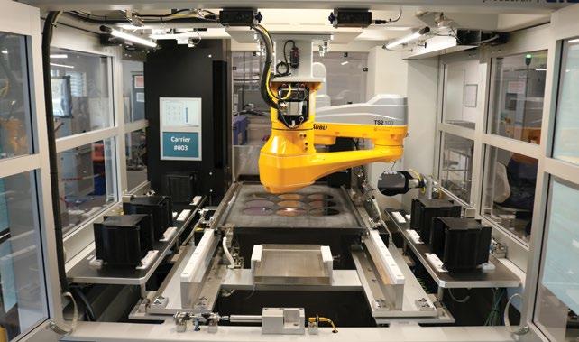
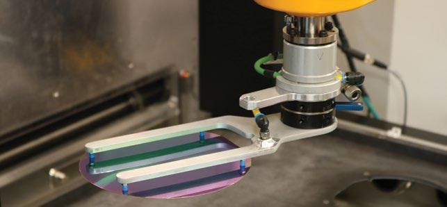
on the ceiling of the loading area of the coating system and has a reach of 1,000 mm. The Scara robot is equipped with a special flat vacuum gripper system that can be quickly exchanged to handle wafers of different sizes.
The robot takes out the wafer from the cassette and places it on a backlit alignment table. A camera system with a 12-megapixel camera is located above the table at a working distance of 680 mm. It detects the exact position of the wafer and sends this information to the Cognex Vision Pro software.
Based on this, the software calculates the position and angle of compensation required to insert the wafer into the carrier nest and transmits the data to the robot controller. Any distortions in the camera system were compensated for, during commissioning, by calibrating it with a checker plate.
In order to overcome the manufacturing tolerances of the carriers and the shrinkage caused by cooling, each workpiece carrier is first centred by pulling it against a stop and indexing it. This allows the coordinate zero point of all carriers in the handling system to be reproducibly defined.
Furthermore, to compensate for manufacturing tolerances, all carriers were accurately measured, beforehand, in their cold, new state and each was given a data matrix code for identification. This code is used to store relevant data in the controller so that the position tolerances of the carrier nests can be calculated and compensated for.
To compensate for the thermal shrinkage caused by the workpiece carriers cooling down, a fiducial mark was first placed in the corner of each carrier opposite the coordinate zero point, and this was also accurately measured precisely when cold. A second camera system is located above this, enabling the offset of the fiducial mark compared to the cold state to be determined.
The software uses this information to calculate the compensation needed to set down the wafer accurately in position. This process
is repeated for each wafer to be inserted.
Flipping station for turning the wafers acp systems also integrated a flipping station for turning the solar cells so that they can be coated on both sides. This receives the corresponding wafers, one by one, from the robot and grips them at defined points with vacuum suction dots. After the wafer has been rotated by 180°, the robot gripper picks it up again and transfers it to the alignment table.
Before the coated solar cells are placed back into the cassettes, a final quality check is carried
out by the camera system on the alignment table. This checks whether the edges of the wafers are free of damage.
The vision-assisted robotic solution, described above, ensures that the extremely delicate solar wafers are handled with high precision and care. This is demonstrated, above all, by the fact that there have been no handling-related wafer breakages since commissioning. Overall, replacing manual handling with a fully automated system has resulted in significantly improved productivity and efficiency.
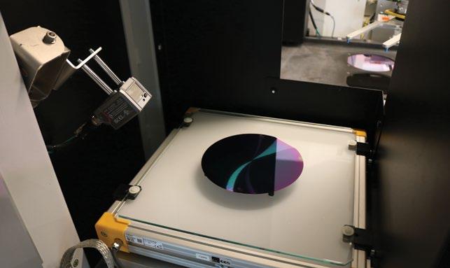
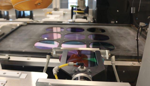
Mikael Carlsson, Global Product Specialist for Indexable Rotating Tools at Sandvik Coromant, explains how a new drilling innovation could reinvent high volume hole making.
High-volume drilling requires precision, efficiency and reliability to meet demanding production schedules and maintain costeffectiveness. For manufacturers, these requirements often pose challenges, such as ensuring tool longevity, achieving consistent hole quality and minimising downtime.
So, what is required to achieve more efficient hole drilling in an increasingly competitive environment?
High-volume hole making often reveals challenges that can be underestimated, even by experienced manufacturers. Many already recognise the critical importance of tool wear and cycle times, but it is the hidden complexities of high-speed and high-penetration operations that can profoundly impact productivity and operational efficiency.
Take, for example, thermal and mechanical stresses encountered during the drilling of thousands of holes – especially in typically more challenging materials like hard steels and heat-resistant super alloys. These forces can lead to accelerated tool fatigue, burr formation or even deformation of the workpiece.
Such challenges go beyond tool durability. They involve understanding the interplay between the tool’s geometry, coatings and material composition, and the specific characteristics of the workpiece. Effective heat dissipation, resistance to microfractures and the ability to maintain edge sharpness over prolonged use are all crucial factors for ensuring consistent quality across extended production runs.
Another consideration is the cost impact of seemingly minor inefficiencies, such as setup or tip changes. In large-scale operations,
for instance, even a small amount of downtime per shift –whether due to recalibrating machines for a new tool or replacing wornout tips – can accumulate into substantial productivity losses. These inefficiencies highlight the importance of streamlined solutions, such as systems designed for quick setup, precise alignment and easy tool changes.
Additionally, eliminating unnecessary steps in the drilling process can drive significant time and cost savings. For example, tools that remove the need for pilot holes or pre-setting equipment can drastically reduce cycle times and minimise the reliance on operator intervention, thereby increasing overall process stability and throughput.
Addressing these pain points with thoughtful planning and optimised tooling strategies is essential for manufacturers striving to meet the demands of high-volume production, without compromising on quality or efficiency.
Introduced by Sandvik Coromant in March 2025, CoroDrill DE10, an advanced exchangeable-tip drill designed for high-volume hole drilling, aims to address these drilling challenges.
CoroDrill DE10 is shown to boost productivity while streamlining operations, due to its advanced -M5 tip geometry. This innovative design achieves an ideal balance between high feed rates and precise penetration, enabling the tool to deliver exceptional performance across diverse materials. From steel alloys to stainless materials, CoroDrill DE10 can ensure consistent hole quality while also minimising the risks of burr formation or workpiece
deformation.
A crucial feature of CoroDrill DE10 is a patented pre-tension clamping interface which combines familiar design with enhanced security. The interface enables fast and easy tip changes without spare parts, ensures reliable drilling at high feeds and speeds, delivers superior clamping strength and achieves straighter holes with tighter tolerances. It also extends drill body life, making CoroDrill DE10 the most robust exchangeable-tip drill of its kind.
Furthermore, CoroDrill DE10 also eliminates the need for pilot holes to further streamline workflows and reduce cycle times and inventory complexity. Its robust design supports extended tool life, with more tips per tool body, which ultimately drives down the cost per hole.
As a plug-and-play solution, CoroDrill DE10 integrates effortlessly into existing setups, making it a practical upgrade for manufacturers looking to enhance productivity without overhauling their systems. It also integrates seamlessly with digital machining systems through Sandvik Coromant’s CoroPlus platform. This compatibility provides operators with precise cutting data and real-time performance insights, so parameter settings can be optimised and tailored to specific materials and applications.
Operational and cost-saving benefits
Several success cases have highlighted how CoroDrill DE10 drastically improves productivity in high volume drilling. In testing conducted in Italy, CoroDrill DE10 demonstrated significant performance advantages over a competing tool while drilling
AISI316L stainless steel.
The case involved 52 mm through and blind holes, using emulsion coolant at 70 bar. CoroDrill DE10 achieved a remarkable 57% increase in productivity and 43% longer tool life compared to its competitor. The tool also delivered excellent hole surface quality, consistent chip control and soundlevel performance aligned with expectations.
The tool’s robust design and advanced -M5 tip geometry ensured reliability and repeatability — and both were key factors for the high-value components in this application. With a higher feed rate, extended tool life and reduced need for downtime, CoroDrill DE10 proved to be a costeffective, efficient and sustainable solution for high-volume drilling in challenging materials.
In another case, an automotive manufacturer faced issues with high cutting forces deforming its drill bodies, specifically while machining gearbox housing components from 47CrMo4 alloyed steel. This issue led to tool failures and increased costs. Instead, switching to CoroDrill DE10 resolved these challenges.
Using a feed rate of 0.35 mm/rev at a depth of cut of 2.5 times the drill diameter, the tool delivered a 17% productivity boost. As in other applications, CoroDrill DE10’s robust design and patented pretension clamping interface ensured exceptional accuracy, extended tool life and minimised downtime.
These examples demonstrate how CoroDrill DE10 meets industry needs while offering significant operational and cost-saving benefits.
High-volume hole-making demands precision, durability and efficiency, making it essential for manufacturers to overcome its challenges to achieve greater productivity and remain competitive. With its advanced features, tools such as CoroDrill DE10 offer a new perspective on drilling and a strategic solution for the future of manufacturing.
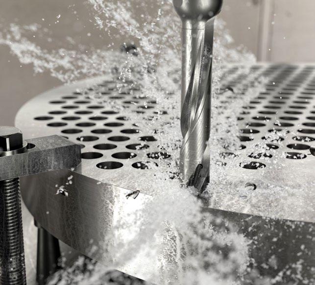

by Andrea Incardona, Application Engineer, Instron
How dynamic drop testing gives material developers confidence in their prototypes’ viability.
The frustration of trusting in a weather app that forecasts a sunny day, only to be drenched with rain, is a feeling that most people have experienced. The same discrepancy occurs in materials characterisation –without the right data inputs, outputs from modelling do not always live up to reality.
Computer aided engineering (CAE) simulations require high-quality, well-defined and extensive data to yield reliable results. A significant amount of early characterisation work involves establishing basic properties such as density, stiffness and tensile strength.
Quasi-static testing remains a fundamental technique for characterising material properties. However, although this method gives reliable outputs at ultra-low velocities, it is less effective for characterising materials under impulsive loads, forcing scientists to extrapolate data gathered at low velocity.
The risk of financial loss from pursuing a material formula that ultimately does not give the required properties is a great concern for materials developers. In many industries that use rigid plastics, films, other polymers and composite materials, the need for 100% reliability in material properties is non-negotiable.
Safety is a key factor too. In safety-critical industries such as aerospace and automotive, dynamic condition testing is often mandated to comply with standards such as the Underwriters Laboratories family.
Take electric vehicles (EV), for example. Within EV batteries, the cell has polyethylene dividing films with selective porosity separating the electrodes. UL2580 demands that this separating polymer is characterised under dynamic conditions to guarantee performance safety.
However, meeting regulatory standards is not the only role of dynamic testing. Advanced instrumentation enables flexible experimental conditions outside standardised frameworks, for example original equipment manufacturers’ (OEMs) internal specifications and allows assessment of different materials.
Resisting technological advances that make dynamic testing more accessible will only see material characterisation struggle to keep up with the evolving demands of relevant sector applications.
Historically, access to dynamic testing instruments has been limited. They are more expensive than quasi-static equipment and this activity has been more niche within the materials characterisation world.
The high-speed nature of dynamic testing requires
great precision to capture material behaviour reliably. Deformation and failure happen within milliseconds, too fast for traditional sensors and data loggers to record. This cheapens the quality of output data, making the overall characterisation profile less accurate.
Several dynamic testing methods exist, each suited to different applications. Split Hopkinson Pressure Bar (SHPB) provides high strain-rate mechanical properties, while Pendulum Impact Testing (PIT) is commonly used for fracture toughness assessment.
When coupled with high-speed imaging or Digital Image Correlation (DIC), these methods can also provide valuable elongation and displacement data. These metrics are important to predict failure modes and identify elastic versus plastic behaviour.
Drop tower tensile impact testing is a developing measurement field that allows material characterisation scientists to find tensile strength, elongation, displacement and the stress-strain curve.
It involves suspending a material coupon in a vice and then dropping a striker at a predetermined velocity to apply longitudinal strain. Similar to other impact systems such as PIT, the dependent variable is the energy absorbed to failure, i.e. until the sample breaks.
Drop tower tensile impact testing provides valuable high strain-rate data, reducing the need for extrapolation from quasi-static tests. Comprehensive profiles do require a combination of drop tower results with other test methods and numerical modelling to predict behaviour across a broad strain-rate spectrum.
Simulations that can be trusted to represent real-world

behaviour not only bring peace of mind to developers over their investments, they also accelerate the pace of advances. In this way, cutting-edge experimentation techniques drive forward technical industries at increasing speeds.
What does drop tower testing add to materials characterisation?
There are multiple technological features that can be applied to drop tower testing that make it appealing for materials characterisation. The first is integration of high-speed imaging. Drop tower instrument manufacturers can pair their machines with high-speed cameras (HSC) to show the failure mode in successive stages, despite the breakage happening in the order of milliseconds.
When combined with a force sensor, failure propagation analysis can show the material sample’s progression from elastic to plastic deformation, it reaching the elongation at break and then the full fracture. This kind of insight is invaluable for predicting real-world behaviour but was not available prior to recent instrumentation advances.
Digital Image Correlation (DIC) is another powerful tool in combination with drop tower tensile impact testing. Although force displacement may be the output value from this test, end-users need a stress-strain curve. While general calculations using impact velocity and percentage deformation give an average strain across the length of the material sample, DIC allows the investigator to characterise localised stress and strain. This is done by applying a visual pattern to a test specimen, such as black dots on a light coloured sample. By exporting the HSC images into dedicated software, users can analyse the movement of the pattern and map stress and strain onto the material’s surface. This granular level of analysis represents a leap forward for materials characterisation and the potential for technological advances.
Finally, variable sampling frequency is essential when considering high-velocity tensile impact testing. Brittle materials, like some composites, break very quickly under high stress. If sampling a brittle material at the higher velocities that dynamic conditions require, for example above 10 metres per second, only a high sampling frequency will allow the tester to detect the force profile at high resolution.
Conversely, a ductile material will have a longer breakage window, perhaps 50 ms compared against 10 ms with the brittle counterpart. A high frequency will not deliver a full failure curve, underlining the importance of variability. For this reason, advanced drop tower instruments have broad sampling frequency ranges and sophisticated data acquisition systems with more than 60,000 acquisition points.
Although quasi-static impact testing is still a useful tool in the arsenal of materials characterisation scientists,
the time to move beyond feeding complex models with approximations has come.
Advanced methods like drop tower tensile impact testing provide surety through experimental data collection. Manufacturing industries can create safer, more reliable products and eliminate the risk involved with investing resources in materials for which they do not have complete characterisation profiles.
With instruments like Instron’s 9450 High Energy Drop Tower, R&D teams can earn an advantage in material development and compliance with standards.
Instron is a leading provider of test equipment for the material and structural testing markets. A global company providing single-source convenience, Instron manufactures and services products used to test the mechanical properties and performances of various materials, components and structures in a wide array of environments.
Instron systems evaluate materials ranging from the most fragile filament to advanced high-strength alloys, providing customers with comprehensive solutions for all their research, quality and service-life testing requirements. Additionally, Instron offers a broad range of service capabilities, including assistance with laboratory management, calibration expertise and customer training.
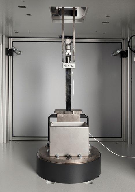
by Hwee Yng Yeo, Industry and Solutions Manager, Keysight Technologies
Researchers must resolve them at the channel and network levels.
As the world anticipates the arrival of applicable 6G innovations, researchers face numerous challenges in validating this nextgeneration wireless communication technology. The journey from theoretical concepts and mathematical equations to realworld 6G implementation is complex and requires meticulous planning, testing and measurements, to better characterise these ultra-high frequencies.
Not only must 6G research help uncover specific channel behaviours – it must also validate how these new frequencies, waveforms and other capabilities will perform from the physical layer up to the higher-layer protocols. Challenges that researchers must resolve are at the channel and network levels.
Channel-level challenges
At the channel level, high-frequency signal propagation issues include path loss, as sub-terahertz and terahertz (THz) bands are prone to significant signal attenuation, losing signal strength over long distances. They also encounter penetration loss where high-frequency signals fade upon encountering obstacles like buildings and foliage, leading to coverage issues.
Atmospheric absorption is also an issue. THz signals are particularly susceptible to absorption by atmospheric gases, reducing signal strength and reliability.
And then there are link budget challenges. The broad bandwidth of 6G signals can lead to low signalto-noise ratios, as energy is spread over a wider frequency range.
Multipath propagation issues include interference and fading. Signals reflecting off surfaces and arriving at the receiver at different
times cause interference and signal distortion. This is exacerbated in urban environments. In fading, rapid fluctuations in signal amplitude due to multipath effects lead to inconsistent signal quality and reduced communication reliability.
In the area of beamforming and beam management, precise beamforming techniques are required to direct high-frequency narrow beams towards the receiver, and beam alignment can be challenging in dynamic environments. Beam tracking presents another challenge, as continuous tracking of the receiver’s location is needed to adjust the beam direction in real-time, adding complexity to the system.
Network-level challenges
Network-level challenges include issues around network density and interference, latency and reliability, and integration with heterogeneous networks.
At the network level, performance depends on how to mitigate issues caused by network density and inter-cell interference, and spectrum management. Dense networks with numerous small cells may increase inter-cell interference, degrading overall network performance. And efficient spectrum management is crucial to minimise interference and maximise the use of available frequencies.
Latency and reliability are also key parameters for achieving ultra-low latency targets (e.g. one-microsecond latency), which require highly efficient signal processing and transmission techniques. There is also a need to ensure reliable 6G communication in diverse environments, including urban, rural and remote areas.

Integration of 6G networks with existing 5G and other wireless technologies requires seamless handover between various network types, and interoperability issues will need to be addressed. Ensuring interoperability between various network components and technologies, such as satellite, terrestrial and aerial networks, is critical for achieving comprehensive coverage and performance goals.
From 6G theory to simulation and emulation
Researchers are modelling various 6G use cases covering channel propagation, waveforms and networks, with design simulation software tools.
The next step in this 6G development process is to take these simulations into real-world signal emulation. Emulation is crucial for testing the performance of 6G systems in real-time channels and networks, from the physical layer to higher layer protocols.
Emulating 6G signals in a controlled lab environment enables researchers to accurately assess the performance of 6G systems. This includes evaluating the challenges cited, under repeatable conditions to fine-tune program iterations against varying scenarios. Researchers can also study system vulnerabilities by emulating cybersecurity issues and addressing them early on.
6G: From innovative research to reality
For instance, Keysight, in collaboration with 6G researchers at Northeastern University in the US, has explored a 130 GHz broadband MIMO system and performed real-time sub-THz research at the network layer,
contributing to the advancement of 6G technology.
The industry expects 6G commercialisation to happen by 2030 – leaving at best five years to bring to fruition both products and applications which must meet conformance standards that are still in various stages of formulation. Researchers, device and component designers, test and measurement specialists, network and cybersecurity engineers, and regulatory authorities are collaborating across the 6G ecosystem to bring 6G to life.

Keysight Technologies Inc, in collaboration with NTT Corporation (NTT) and NTT Innovative Devices Corporation (NTT Innovative Devices), recently announced a groundbreaking world record in data rate achieved using subterahertz (sub-THz) frequencies.
This milestone was reached with Keysight’s Vector Component Analyzer (VCA) in conjunction with NTT’s and NTT Innovative Devices’ high-output, wide-bandwidth J-band Indium Phosphide (InP)based power amplifier (PA). In addition, advanced digital predistortion techniques were employed to mitigate amplifier non-linearities, ensuring robust, high-fidelity signal generation.
The rapid advancement of 6G, AI and autonomous driving technologies is driving a significant demand for wide bandwidth capabilities offered by sub-THz frequencies for high-speed wireless communication and precision radar sensing. Validating these systems with high-quality modulated signals is essential for development and deployment. However, achieving highquality signals in the sub-THz range has been challenging due to the complexities of amplifying signals and managing distortion at higher power levels.
The collaboration between

Keysight, NTT and NTT Innovative Devices demonstrated the power amplifier’s effectiveness in the 300-GHz frequency band. Testing confirmed its saturated power level at +9.1 dBm and achieved a 280 Gbps data rate (35 GBaud 256 QAM) at 0 dBm power output – the highest data rate reported in the 300 GHz band.
This is largely attributed to Keysight’s Vector Component Analyzer, built on the latest N524XB series PNA-X Microwave Network Analyzers equipped with digital predistortion techniques, which optimised signal integrity and minimised distortion to enable the high data transmission speed.
Hirokazu Takenouchi, Vice President, Head of NTT Device Technology Laboratories, said, “At NTT, we are consistently advancing
the limits of carrier frequency and integration within radio systems. These developments are pushing the boundaries of what can be achieved in wireless communication systems.”
Akimasa Kaneko, Executive Vice President of NTT Innovative Devices, Photonic Components Business Group, said, “By utilising our InP technology and collaborating with several partners, we have achieved a remarkable maximum throughput of 280 Gbps.”
Joe Rickert, Vice President and Head of Keysight’s High Frequency Center of Excellence, said, “This 280 Gbps world record underscores Keysight’s commitment to providing the advanced test and measurement solutions critical for unlocking the potential of sub-THz frequencies for 6G.”
by Takanori Nishiyama, Senior Vice President of APAC & Japan Country Manager, Keeper Security
Addressing a rapidly evolving threat landscape.
In cybersecurity, credentials function like keys to a building –anyone holding them has access. That is why it is not enough to simply secure access credentials. We must also ensure they are used by the right individuals, for the right purposes and even at the right time.
Former Intel CEO, Dr Andrew Grove famously said, “Only the paranoid survive.” In today’s cyber threat landscape, this mindset could not be more relevant.
Adopting a zero-trust approach –where nothing is assumed safe and all access is verified – is no longer optional. It is essential.
This is particularly true for the Asia Pacific region, where highprofile breaches across the financial sector – from Australia to Japan and Singapore – have exposed both consumer and institutional data. Financial institutions, just like any industry player, face complex supply chain risks that demand robust controls at every point of access.
While many institutions have taken comprehensive steps to implement and constantly improve cyber defences, one area stands out that needs more attention. Many organisations have yet to invest in a privileged access management (PAM) solution, perhaps due to a perceived high cost and complexity. While this may be true for certain historical PAM solutions, these organisations may have overlooked the advantages that contemporary PAM solutions provide.
1 Gain full visibility into your network
Without privileged access control, it is easy for users to accumulate excessive access rights, often more than they need. This not only increases your attack surface but makes it difficult to detect suspicious activity. PAM gives IT teams visibility into who is accessing what, when and how. Real-time session monitoring and logging make it possible to quickly identify and respond to anomalies.
2 Prevent privilege abuse
Privilege abuse – when insiders misuse elevated access – is a serious and often undetected threat. PAM solutions mitigate this risk through privileged session management which records, monitors and restricts sensitive sessions to prevent unauthorised activities.
3 Simplify regulatory compliance
Compliance frameworks such as HIPAA, PCI DSS, SOX and APACspecific regulations increasingly mandate least-privilege access and traceability. PAM helps enforce the Principle of Least Privilege (PoLP) and provides centralised audit trails, making it easier to meet audit requirements and reduce compliance risk.
4 Boost IT and employee productivity
Modern PAM solutions reduce the time IT teams spend manually

provisioning accounts or resetting credentials. Through centralised dashboards and automated password management, PAM improves operational efficiency while giving employees faster, more secure access to the tools they need.
5 Reduces costly configuration errors
Manual configuration often leads to users receiving broader access than necessary. PAM automates access provisioning and enforces policy consistency, reducing the risk of misconfigurations that can open the door to attackers.
6 Reduce your attack surface
Every unused credential or overlypermissioned account represents a potential vulnerability. PAM limits access to only what is necessary, minimising exposure if credentials are compromised. Integrated password management further strengthens security by eliminating weak or reused passwords.
7 Improve breach containment
In the event of a breach, PAM plays a critical role in containment. By restricting lateral movement through least privilege enforcement, attackers are less able to escalate privileges or access multiple systems – making incidents easier to isolate and mitigate.
8 Strengthen your cyber insurance profile
As cyber insurance providers raise the bar on security prerequisites, PAM has emerged as a core control.
Demonstrating the use of PAM can help businesses qualify for coverage and potentially reduce premiums by showing a mature risk profile.
While legacy PAM solutions were often costly and complex, today’s cloud-based offerings are more accessible. They reduce the need for manual oversight, protect critical assets and support a stronger case for cyber insurance –all of which help lower security and compliance costs over time.
Not all PAM tools are created equal. To get the most value from your
investment, organisations should prioritise these key features:
• Zero Trust Architecture – Choose a solution grounded in zero trust principles. Never assume trust, always verify and enforce least privilege. This ensures that every access request – human or machine – is authenticated and authorised.
• Cloud-Based Infrastructure – A modern PAM platform should be cloud-native to support today’s hybrid work environments. Cloud delivery offers easier updates, greater scalability and remote access without the overhead of onpremise systems.
• Fast Deployment – Look for a solution that is quick to deploy and does not require additional
hardware or complex integrations. The faster it is up and running, the sooner your organisation is protected.
With privileges come responsibilities – and risks. In a region as dynamic and digitally connected as the Asia Pacific region, the stakes are high. From cyber attacks to regulatory fines to reputational harm, unmanaged privileged access is a vulnerability no business can afford. By investing in a zero trustbased PAM solution, organisations gain visibility, control, compliancereadiness and long-term savings –while building resilience in a rapidly evolving threat landscape.
Keeper Security, a leading cybersecurity provider of zero-trust and zero-knowledge Privileged Access Management (PAM) software protecting passwords, passkeys, privileged accounts, secrets and remote connections, recently announced an update to its password management platform.
Keeper’s upgraded OneTime Share feature enables bidirectional, single-use encrypted sharing between Keeper users and non-users, providing customers with a secure way of exchanging confidential information with their customers, vendors and partners.
The new bidirectional sharing feature builds upon the functionality of Keeper’s existing One-Time Share (OTS) feature. OTS is designed to securely share credentials and files with a selected recipient for one-time use. These shares are protected in transit by Keeper’s ellipticcurve and AES-256 cryptography and can only be decrypted locally on the recipient’s device. Once received, shared records automatically expire based on the sender’s specified time. Additionally, each share is
restricted to a single device, allowing the recipient to access the shared data multiple times until it expires or the sender terminates the share – whichever occurs first.
“Bidirectional One-Time Share is the latest step in our commitment to ensuring that all customers can simply and securely exchange confidential information with end-to-end encryption,” said Craig Lurey, CTO and Co-Founder of Keeper Security.
“By adding bidirectional editing support, we add yet another layer of security to our users’ cyber defences. We are proud to be the first in the industry to add this capability and continue supporting our customers, first and foremost,” he added.
The bidirectional functionality update allows easier sharing between users and non-users of Keeper’s platform. Previously, users were able to send viewonly external shares. Now, non-users can also exchange data with Keeper customers, offering end-to-end encryption for both parties. This powers the secure collection and exchange of confidential information such
as documents and credentials –without having to use insecure email, text messages or instant messaging channels.
Users share records by selecting the desired record from their Keeper Vault and initiating a onetime share. The user can then customise the access settings and generate a secure, time-limited link. The recipient clicks the link to view the content, where they can upload, modify or comment as needed. Once the time limit is reached or access is revoked, the session ends permanently and the record is no longer accessible.
Organisations can use the bidirectional one-time share to facilitate operations such as:
• Collaboration: Securely collect signed documents, feedback or sensitive files from clients, contractors and partners, without needing them to create an account.
• Vendor Requests: Request compliance documents or private credentials from third parties securely.
• Internal Audits: Temporarily share and retrieve information with auditors or legal teams.
The report finds 65% of organisations suffered a cloud-security incident in the past year – yet only 6% remediated it within an hour.
Check Point Software Technologies Ltd, a pioneer and global leader in cybersecurity solutions, recently released its 2025 Cloud Security Report. Based on a global survey of more than 900 CISOs and IT leaders, the report reveals systemic weaknesses, including alert fatigue, fragmented toolsets, and a widespread inability of organisations to detect lateral movement or defend against AI (artificial intelligence)-driven attacks, leaving enterprises dangerously exposed. The findings also include actionable strategies for closing the gap between cloud innovation and cyber resilience.
As hybrid, multi-cloud and edge architectures expand, many organisations are relying on outdated security models that cannot keep up. According to the report, 65% of organisations experienced a cloud-related security incident in the past year – up from 61% the previous year. Alarmingly, only 9% detected the incident within the first hour, and a mere 6% managed to remediate it within that time frame, allowing intruders to remain undetected across cloud environments.
“Security teams are chasing an ever-moving target. As cloud environments grow more complex and AI-driven threats evolve, organisations cannot afford to be stuck with fragmented tools and legacy approaches. It is time to shift toward unified, intelligent, and automated defences designed for the realities of today’s decentralised world,” said Paul Barbosa, VP of Cloud Security at Check Point Software Technologies.
Key findings from the 2025 Cloud Security Report include the following:
• Cloud adoption outpaces security readiness: 62% of organisations have adopted cloud edge technologies, 57% use hybrid cloud, and 51% operate in multicloud environments. Legacy, perimeter-based defences cannot keep up with these distributed infrastructures.
• Detection and remediation are too slow: Only 9% of organisations detected an incident within the first hour. Meanwhile, 62% took more than 24 hours to remediate breaches, giving attackers ample time to escalate access.
• Tool sprawl is fuelling alert fatigue: A significant 71% of respondents rely on over 10 different cloud security tools, while 16% utilise more than 50. More than half of them face nearly 500 alerts daily, hindering response times and overwhelming analysts.
• Application security lags behind: 61% still rely on outdated, signature-based Web Application Firewalls (WAFs), which are increasingly ineffective against sophisticated, AI-enhanced threats
• AI is a priority, but defenders are not ready: While 68% list AI as a top priority for cyber defence, only 25% feel prepared to counter AIdriven attacks, highlighting a critical capability gap.
• Lateral movement remains a blind spot: Only 17% of organisations have full visibility into east-west cloud traffic. Once attackers breach the perimeter, they can move undetected within cloud environments.
• Detection often comes from people, not tools: Only 35% of cloud incidents were detected via security monitoring platforms. The
majority were identified through employees, audits or external reports – revealing alarming gaps in real-time threat detection.
• Internal challenges undermine progress: 54% cite the pace of technological change as a major hurdle, while 49% face a shortage of skilled security professionals. Tool fragmentation and poor platform integration (40%) further slow response times and exacerbate blind spots.
To close these gaps, Check Point recommends a shift towards decentralised, prevention-first cloud security strategies. The report advises organisations to consolidate their toolsets, adopt AI-powered threat detection, and deploy real-time telemetry to gain full visibility across edge, hybrid, and multi-cloud environments. By leveraging Check Point CloudGuard and the Check Point Infinity Platform, organisations can unify their cloud defences, automate incident response, and ensure consistent policy enforcement – regardless of platform or provider.
The 2025 Cloud Security Report, carried out by Cybersecurity Insiders in the beginning of 2025, gathered insights from 937 cyber security professionals across North America, Europe, Asia-Pacific, and other regions. Respondents included CISOs, cloud architects, security analysts, and IT leaders responsible for securing hybrid, multicloud, and SaaS environments. The study focused on how businesses using cloud services tackle security issues and highlight advancements, like AI, emphasising the complexity of modern cloud security.
Long cable runs from variable speed drives (VSDs) to motors are common in industrial environments. While this design provides flexibility in terms of system layout, it can create issues of electrical noise and interference that severely impact system reliability. If not addressed, these problems can lead to overheating, failures and downtime.
David Strain, Technical Director at Technidrive, an automated systems specialist, explains how these challenges can be mitigated.
Long cable runs are common in large facilities like manufacturing plants, water treatment stations, mining operations and offshore platforms. These systems are typically spread over wide areas, with motors often located far from variable speed drives (VSDs), requiring connections back to centralised hubs or control centres.
Longer cable runs can act like antennas, making them more likely to pick up stray electromagnetic signals than shorter runs. Additionally, the increased cable length can introduce capacitance and resistance – storing and slowing down the flow of electricity and amplifying the effect of interference on the signal. These unwanted reflective waveforms impact system efficiency, increase power consumption and can lead to overheating.
Another consequence of these issues is unnecessary shutdowns in equipment like VSDs. This is otherwise known as a nuisance trip, where the system cuts out unexpectedly. Nuisance trips can have serious consequences in industries like food processing, where temperature control is crucial. A minor interruption in a cooling system, for instance, can result in food spoilage, consequent financial losses and health risks.
Cable run management
What can engineers do to avoid these issues? An answer is improving the management of longer cable runs. One methodology is to use shielded cables to reduce interference, while
carefully routing them away from sources of noise. Another option is to keep cable lengths optimal, while ensuring they are supported and protected against mechanical stresses.
Regular inspections and proper grounding are also key to maintaining efficiency and avoiding system failures.
In addition to these methods, reactors can provide another solution. Also known as motor chokes, reactors are large inductors that are installed at the output of a VSD. They absorb and smooth out electrical noise and interference that occurs as electrical signals travel along cables and, in doing so, ensure that the motor runs cooler and the system operates stably and efficiently. As a result, false overcurrent trips and cable overheating can be avoided.
Technidrive recommends reactors for cable runs over 80 m in length when using a VSD. However, even shorter cable runs may require reactors if multiple motors are connected to a single VSD, as the cumulative length of cables can create electrical interference.
Let us look at an example of these technologies in use.
A food processing plant was experiencing frequent nuisance trips in its cooling system. Given that the cooling fans were essential for maintaining the right temperature for perishable items, the disruptions were a problem.
The food processor approached Technidrive to help solve the issue. The plant’s system involved multiple motors running from a
single WEG CFW 11 VSD with long cable runs. However, electrical interference led the VSD to mistakenly detect overcurrent conditions. This caused the system to shut down unexpectedly and halt the cooling process.
To select the right reactor for this application, Technidrive’s specialists advised it was crucial to match the reactor’s current rating with the VSD’s maximum current. For instance, if the VSD is rated for a maximum current of 10 amps, a reactor capable of handling this current should be chosen. This ensures the reactor can effectively absorb electrical noise and interference without being overstressed.
For the plant, Technidrive’s engineers recommended that a REO motor choke (CNW854) be installed at the output of the VSD. Its specifications include a voltage rise limitation of <200 volts per microsecond (V/µs), noise reduction capabilities, fully encapsulated design for protection up to IP 66, and the ability to support longer motor cable lengths without introducing additional interference. The result? The reactor absorbed the electrical noise and eliminated the reflective waveforms, preventing false trips.
This example demonstrates how reactors play a vital role in maintaining reliable performance, particularly in systems with long cables or multiple motors. However, it is essential to consult experts to ensure that the correct reactor is chosen and properly installed.
by Jitender Khurana, General Manager, Systems and Services, Asia Pacific and Marco Scaioli, Director of DZE Asia Pte Ltd


Innovative lighting solutions for global sports events such as the Singapore Grand Prix.
As the world continues to address pressing environmental challenges, Formula 1 and event promoters are now focused on reducing their carbon footprint.
With regard to night races, the spotlight has turned to one of the most essential elements of such events – the lighting.
The Singapore Grand Prix – the first of six circuits to hold a night race – is more than just a spectacle of speed and skill. Since its debut in 2008, it has also become a testing ground for sustainability efforts in global sports.
With a mission to halve their energy emissions by 2028, the Singapore Grand Prix organisers have set out to reduce the event’s environmental footprint, with a series of initiatives that focus on energy reduction and increasing the use of renewable energy. An example of this effort is the innovative approach to lighting.
THE SINGAPORE GRAND PRIX
Lighting a temporary track, like the Marina Bay Street Circuit, involves overcoming several hurdles. Unlike permanent racetracks, where lighting infrastructure is fixed year-round, the 4.94 km long track, for the Singapore Grand Prix, requires engineers to install a fully operational lighting system from scratch, each year. The precision required in positioning and maintaining these lights cannot be overstated, given the high speeds at which Formula 1 cars race and the need for absolute clarity in terms of visibility.
In recent years, the race’s lighting

system has evolved to reflect broader sustainability goals. The Fédération Internationale de l'Automobile (FIA) has committed to making Formula 1 a net-zero carbon sport by 2030, emphasising energy efficiency as a key priority in achieving this goal. The challenge lies in meeting these targets, while still delivering the powerful, consistent illumination needed to ensure driver safety and the race’s visual spectacle.
The move to advanced LED lighting systems has been instrumental in the Singapore Grand Prix’s drive to sustainability. These lights consume significantly less energy than traditional metal halide systems – cutting power consumption by up to 30% –without sacrificing performance.
There is also the challenge of ensuring that the lighting meets the demanding safety and broadcast requirements set by FIA.
Technical lighting challenges Formula 1 cars can reach speeds of over 300 km/h, which makes visibility an absolute priority.
The lighting must allow drivers to clearly see the track, their competitors and any potential hazards, without distractions caused by glare, shadows or inconsistent lighting. Achieving this requires advanced technical precision and a comprehensive plan by the appointed lighting consultants, DZE Asia Pte Ltd, a sister company of DZ Engineering (DZE).
The lighting system is designed to mimic natural daylight, with a colour temperature of 5700 K and a high colour rendering index. This ensures that the lighting is not only bright enough but also offers a uniform quality that allows drivers to read the track as though it is daylight. The critical factor here is uniformity – any inconsistencies in lighting levels can distort drivers' perception of speed and distance, increasing the risk of accidents.
In contrast to permanent circuits, where lighting masts can rise up to 40 m, the Singapore Grand Prix uses temporary trusses at a lower height of 10 m. This presents a unique challenge – how to evenly distribute light across
the track from such a low angle, without creating unwanted glare or shadows. Engineers must carefully adjust the positioning and angles of the lights, to ensure the track is uniformly lit. Even small adjustments in positioning can have a dramatic effect on visibility, particularly in areas where drivers must make split-second decisions.
Minimising light pollution and protecting the environment
In addition to the technical challenges of performance, the lights used for the race must be designed to minimise light pollution – specifically spill light, glare and sky glow.
To tackle this, the lighting system uses highly directional beams that focus light solely on the track, significantly reducing the amount of light that escapes into the surrounding area. This precision not only reduces light pollution but also contributes to the sustainability goals of the event, by ensuring that no unnecessary energy is wasted as a result of lighting areas that do not need it.
Enhancing spectator and broadcast experience
Lighting does not just play a functional role. It also shapes the visual appeal of the event for spectators and broadcasters.
The Singapore Grand Prix, as a night race, depends heavily on its lighting system to create a visually compelling experience for millions of viewers around the world.
For television broadcasts, consistency and quality of light are critical. The system must meet the latest broadcasting standards to ensure that there is no flicker or glare on camera, which could detract from the viewing experience. The challenge is to provide uniform, high-quality light that enhances the fast-paced action on the track, while capturing the vibrant backdrop of Singapore’s skyline.
At the same time, spectators in the stands need to feel immersed in the race. The lighting is designed

not just for function but also for spectacle – turning the race into an unforgettable night-time event where the track and the surrounding cityscape are both highlighted.
Lighting system revamp by DZE and Signify
As the official Singapore Grand Prix vendor, DZ Engineering (DZE) led the revamp of the lighting system for the Marina Bay Street Circuit, with Signify as a key partner for the design and supply of LED lighting solutions.
DZE managed the technical design and installation, ensuring the seamless setup of over 1600 LED floodlights.
Signify’s cutting-edge, energyefficient LED technology helped reduce energy consumption by up to 30%, while maintaining the high safety and visibility standards required for Formula 1. Together, DZE and Signify delivered a visually captivating race experience with minimal environmental impact, contributing to the Grand Prix’s broader sustainability objectives.
The Singapore Grand Prix is setting the standard for how advanced lighting solutions can help meet the sustainability demands of global sporting events. By incorporating energy-efficient LED technology, minimising light pollution and overcoming the unique technical challenges of a temporary circuit, the race offers a glimpse into

The lighting system, based on energyefficient LED technology, mimics natural daylight with uniform quality.
the future of sustainable event management.
As Formula 1 continues its drive toward net zero carbon emissions, lighting will play a central role in ensuring that the sport can balance performance with environmental responsibility. The lessons learned from lighting the Singapore Grand Prix will likely influence other major global events, from sports tournaments to large-scale concerts, as cities and industries strive to reduce their environmental impact, while delivering world-class experiences.
Lighting, once considered a functional aspect of event planning, has now become a crucial factor in the sustainability narrative, showing that even in the high-speed, highstakes world of Formula 1, lighting technology can illuminate the path to a greener future.
XP Power hopes to revolutionise the configurable, modular power supply market with the introduction of its FLXPro series.
The FLX1K3 is a 1.3 kW configurable chassis mount AC-DC power supply designed to simplify power systems for healthcare, industrial applications, semiconductor manufacturing, analytical instrumentation, automation, renewable energy systems and robotics.
Housed in a compact 1U form factor, measuring 254.0 mm x 88.9 mm x 40.6 mm (10.0” x 3.50” x 1.6”), the FLXPro series delivers power levels of 1.3 kW at high line conditions and 1 kW at low line, with power density of up to 23.2W/in³. Its compact size and high power density reduce end application size and complexity, addressing application space constraints and the need for increased power. Designed with SiC/GaN technology and a fully digital architecture, the FLXPro achieves efficiencies up to 93%, reducing operating costs and cooling requirements.
Flexibility and controllability are central to the FLXPro’s design. It features up to four customerselected, inherently flexible output modules with selectable outputs from 9 VDC to 66 VDC and a wide adjustment range (+10% to -40%), which can be configured under live conditions to form part of a customer’s active control system. Output modules can be combined into multiple parallel and series configurations, and multiple FLXPro units can also be combined in parallel for higher power applications. This inherent flexibility optimises application performance and control, addressing customer requirements for fixed and variable loads.
A key differentiator for the FLXPro series is its fully digital architecture, covering both the input stage and the output modules. This digital infrastructure is the foundation for XP Power’s new iPSU Intelligent Power technology which translates

rich internal data into usable information, enabling users to make fast, quality decisions that improve application safety and reduce operating costs.
XP Power’s iPSU technology is enhanced by XP Power’s latest intuitive user interface, XPInsight. Developed using human-centred design (HCD) principles, it simplifies system configuration, monitoring and control, and has advanced capabilities like graphing, datalogging and simultaneous multi-unit display. This HCDoptimised UI facilitates fast, quality decisions regarding the power supply application state and provides intuitive status, health and configuration information.
It also incorporates multi-level password protection and cybersecurity features for improved security. By streamlining power supply setup and customisation, XPInsight helps accelerate development timelines and reduce engineering costs.
The FLXPro series provides extensive and unique diagnostics, including a new Black Box Snapshot feature that reduces troubleshooting time after shutdown events by recording in-depth system status at, and prior to, shutdown.
Additionally, tri-colour LEDs indicate power supply health with a truth table incorporated on the chassis for fast, simple interpretation without manuals or digital communications. Multiple internal temperature measurements enable fast status checks through extensive temperature diagnostics that drive intelligent fan control and over
temperature warnings and alarms.
Inputs, outputs and firmware can be configured through the UI or directly over direct digital communications, enabling application design flexibility and tailored system integration. This allows for quick adaptation to changing application needs during design, test and in-life operation, reducing both development timescales and system costs.
FLXPro includes in-built, userdefined digital controls, signals, alarms and output controllability which contribute to an optimised system design and application health visibility that enables reduced maintenance/testing times and operating costs.
The FLXPro series supports ES1 isolated digital communications which improves application safety while reducing integration complexity and supply damage risks. FLXPro uses PMBus over I²C for digital communications, enabling real-time control, monitoring and datalogging. Standard external connectivity is provided for output modules and the system chassis including AC OK, DC OK, remote inhibit (global/module), fan fail/temp warning, sync, and current share.
The FLXPro series conforms to medical and ITE safety approvals, including 2 x MOPP isolation for medical applications. The series is SEMI F47 compliant and meets various immunity and emissions standards, including EN61000-4 immunity and EN55011/EN55032 Class B for conducted and radiated emissions.
Metis Engineering, a leader in innovative engineering solutions, has announced the launch of its latest product, the Analogue to Digital CAN Module. This cutting-edge device is designed to seamlessly convert analogue signals into digital data, facilitating enhanced integration with Controller Area Network (CAN) systems across a wide range of industries, including automotive, marine, aerospace, marine energy storage and industrial automation.
The 12 bit 8 channel Analogue to Digital CAN Module is capable of measuring 0-5 V signals in precise 0.003 V increments, with sampling rates of up to 333 Hz. A 10 kΩ pull-down resistor on each channel enables direct connection to resistance-based temperature sensors without the need for additional components.
In addition to analogue input, the module supports pulse-width modulation (PWM) duty cycle and frequency measurement, digital input status, and includes a pulse counter, ideal for applications such as traction control. The module also includes a low power sleep mode consuming less than 1 mA, with the ability to wake on voltage thresholds, making it suitable for use as a CAN wake-up device via external triggers such as a button press.
Its compact design ensures easy integration into existing systems, while robust construction and an automotive IP67-rated connector offer high reliability even in harsh environments. The configurable CAN bus speed and address, along with a supplied DBC file, allow for straightforward integration into virtually any CAN network.
“Our new Analogue to Digital CAN Module addresses the growing need for efficient and accurate data conversion in modern engineering applications. By offering a reliable solution for integrating analogue

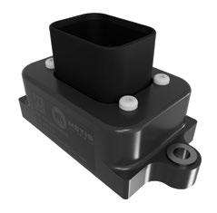

The Analogue to Digital CAN Module is designed to seamlessly convert analogue signals into digital data.
inputs into digital CAN systems, we empower our clients to enhance the performance and efficiency of their operations,” said Joe Holdsworth, Founder and CEO at Metis Engineering.
The module is compatible with a wide range of sensors and devices, making it suitable for a host of applications requiring precise data acquisition and transmission. Its plug-and-play functionality simplifies installation, reducing downtime and
implementation costs.
Metis Engineering also offers complementary products, such as the Nano Development Kit and the R&D Development Kit, to support the evaluation and integration of their CAN-based sensors and modules. These kits provide all necessary cables and features to facilitate seamless connection and testing within CAN networks.
The Analogue to Digital CAN Module is manufactured in the UK.
Aerotech Inc, a global leader in precision motion control and automation, recently announced the release of DrillOptimizer, an advanced AeroScriptPlus feature for galvo scanner systems.
Designed for equipment manufacturers using laser drilling with high-dynamic point-topoint motion, DrillOptimizer tackles the complex challenge of optimising step and settle motion for thousands to millions of hole locations, minimising overall drilling cycle time and maximising galvo scanner hardware performance.
“Optimising high-dynamic point-to-point motion for laser drilling applications with varying hole distances has long been a demanding task,” said Aerotech Product Manager, Bryan Germann.
“We created DrillOptimizer so our customers can save development time and increase throughput without sacrificing on precision,” he added.
DrillOptimizer works in two, key ways:
• Motion Sequence Optimisation: DrillOptimizer intelligently determines the most efficient path through a pattern of holes, whether within a single scanner field of view (FOV) or when combined with a servo stage system using Infinite Field of View (IFOV).
This path optimisation directly minimises the overall cycle time by ensuring the shortest travel distance for the scanner.
• Step and Settle Optimisation: DrillOptimizer enables optimal
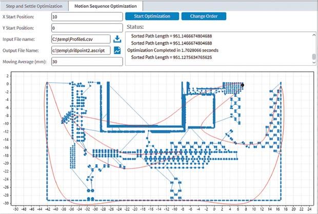
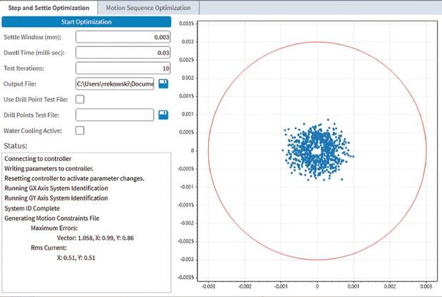
DrillOptimizer works through Motion Sequence Optimisation and Step and Settle Optimisation.
controller parameters to be used for any specific step distance without the scanner leaving the user-defined settle window.
By identifying the ideal parameters for each move based on the user-specified settle window and laser-on time, settling move delays are eliminated – allowing the laser to fire with zero delay if the scanner remains within the settle window.