MEMORY CHIPS WITHSTAND EXTREME HEAT PORTABLE KNITTED ANTENNAS NON-TOXIC SOLAR CELLS – THE FUTURE OF ENERGY STORAGE?


MEMORY CHIPS WITHSTAND EXTREME HEAT PORTABLE KNITTED ANTENNAS NON-TOXIC SOLAR CELLS – THE FUTURE OF ENERGY STORAGE?

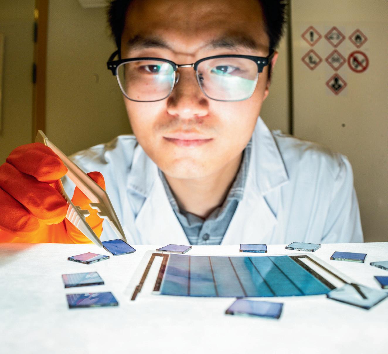
An eco-friendly, high-performance organic battery is being developed by scientists at UNSW Sydney.
Ateam of scientists at UNSW Chemistry have successfully developed an organic material that is able to store protons — and they have used it to create a rechargeable proton battery in the lab.
By leveraging hydrogen ions — protons — instead of traditional lithium, these batteries hold promise for addressing some of the critical challenges in modern energy storage, including resource scarcity, environmental impact, safety and cost.
The latest findings, recently published in the journal Angewandte Chemie , highlight the battery’s ability to store energy quickly, last longer and perform well under subzero conditions.
The material — tetraamino-benzoquinone (TABQ) — developed by PhD candidate Sicheng Wu and Professor Chuan Zhao, in collaboration with UNSW Engineering and ANSTO, has been shown to support rapid proton movement using hydrogen-bond networks.
“We have developed a novel, high-capacity small-molecule material for proton storage,” Zhao said. “Using this material, we successfully built an all-organic proton battery that is effective at both room temperature and sub-zero freezing temperatures.”
Batteries store chemical energy and convert it to electrical energy through reactions between two electrodes — the anode and cathode. Charge-carrying particles, known as ions, are transferred via the middle component of the battery, known as an electrolyte.
The most common type of batteries used in household products are lithium-ion batteries. These batteries, which create an electric charge by transferring lithium ions between the anode and cathode, are the most widespread portable energy storage solutions.
Lithium-ion batteries power everyday products such as mobile phones, laptops and
smart wearables, as well as newer e-mobility products such as electric cars, e-bikes and e-scooters. However, they are very difficult to recycle and require huge amounts of water and energy to produce.
“Lithium-ion batteries are already becoming a dominant product in energy storage applications, but they have a lot of limitations,” said Sicheng Wu, a PhD candidate from the School of Chemistry.
“Lithium is a finite resource that is not evenly distributed on earth, so some countries may not have access to low-cost lithium sources. Lithium batteries also have very big challenge regarding fast-charging applications, safety, and they have low efficiency in cold temperature.”
Although we currently rely very heavily on lithium-ion batteries, a growing number of alternatives are emerging.
Proton batteries are gaining attention as an innovative and sustainable alternative in the energy field, and have been hailed as one of the potential solutions to next-generation energy storage devices.
Protons have the smallest ionic radius and mass of all elements, which allows them to diffuse quickly. Using protons results in batteries with high energy and power density, plus, protons are relatively inexpensive, produce zero carbon emissions and are fast charging.
“There are many benefits to proton batteries,” Wu said. “But the current electrode materials used for proton batteries, some of which are made from organic materials, and others from metals, are heavy and still very high cost.”
While a few organic electrode materials already exist, they also suffer from limited voltage range, and further research is required to make them viable batteries.
Redox potential is a fundamental parameter in electrochemistry. It’s related to the flow of electricity, which is important for designing batteries. The range of redox potentials in a battery is important because it affects the battery’s performance. Usually, the redox potentials of cathode materials need to locate in a high range and that of anodes needs to locate in a low range to ensure a desirable battery voltage output.
To create their electrode material, the research team started with a small molecule, called Tetrachloro-benzoquinone (TCBQ), which includes four chlorine groups. Although TCBQ has been used previously to design electrode materials, the redox potential range of this compound is mediocre — neither low enough to be used as anode nor high enough as cathode.
So, to start, the team set out to modify TCBQ to increase its performance as an anode material.
After multiple rounds of modifications of the compound, the researchers settled on replacing the four chloro groups with four amino groups, making it a tetraaminobenzoquinone (TABQ) molecule. By adding amino groups, the researchers significantly improved the material’s ability to store protons and lower its redox potential range.
“If you just look at the TABQ material that we have designed, it’s not necessarily cheap to produce at the moment,” Zhao said. “But because it’s made of abundant light elements, it will be easy and affordable to eventually scale up.”
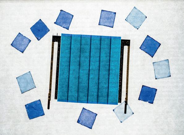
When the researchers tested the proton battery, the results were extremely promising.
Combined with a TCBQ cathode, the all-organic battery offers long cycle life (3500 cycles of fully charging, and then fully draining the battery), high capacity, and good performance in cold conditions, making it a promising step for renewable energy storage.
“The electrolyte in a lithium-ion battery is made of lithium salt, a solvent which is flammable and therefore is a big concern,” Zhao said. “In our case, we have both electrodes made of organic molecules, and in between we have the water solution, making our prototype battery lightweight, safe and affordable.”
“At the moment, we don’t have any suitable solutions to grid-scale energy storage, because we can’t use tons of lithium batteries
PROTON BATTERIES ARE GAINING ATTENTION AS AN INNOVATIVE AND SUSTAINABLE ALTERNATIVE IN THE ENERGY FIELD, AND HAVE BEEN HAILED AS ONE OF THE POTENTIAL SOLUTIONS TO NEXT-GENERATION ENERGY STORAGE DEVICES.
to do that job, due to the price and lack of safety,” Wu said.
Given the low cost, high safety and the fast charging performance of the proton battery designed through this collaboration, it has the potential to be used in a variety of situations, including grid-scale energy storage.
“To enhance the usage of renewable energies, we have to develop some more efficient energy integration technologies and our proton battery design is a promising trial,” Wu said.
While the potential applications are vast, the researchers are determined to refine and perfect their proton battery.
“We have designed a very good anode material, and future work will move to the cathode side. We will continue designing new organic materials that have higher redox potential range to increase the battery output voltage,” Wu said.
Zhao also noted that what he was most excited about was the unique mechanism of proton transport they had identified. “Proton transport is one of the most fundamental processes in nature, from the human body, to plants,” he said. “We can actually study how this type of organic molecule can be used for a broad range of applications, such as for hydrogen storage.
“Molecular hydrogen (H2) is very reactive and therefore difficult to store and transport. This is currently a bottleneck for the hydrogen industry. However, hydrogen also exits in a stable form: proton (H+).”
The development of materials to store protons, means hydrogen can easily be shipped around the world, and then extracted when and where it is needed. “Our discovery has made this concept a possible reality,” he added.

A new technology that can generate electricity from vibrations or even small body movements means you could charge your laptop by typing or power your smartphone’s battery on your morning run.
Researchers at the University of Waterloo have developed a tiny, wearable generator in response to the urgent need for sustainable, clean energy. It is also scalable for larger machines.
“This is a real game changer,” said Dr Asif Khan, the project’s lead researcher and a postdoctoral fellow in the Department of Electrical and Computer Engineering at Waterloo. “We have made the first device of its kind that can power electronics at low cost and with unprecedented efficiency.”
The device uses the piezoelectric effect, which generates electrical energy by applying pressure to materials like crystal and certain ceramics. Piezoelectric materials are currently used in various sensing technologies including sonar, ultrasonic imaging and microwave devices.
“Those older materials are brittle, expensive and have a limited ability to generate electricity,” said Dr Dayan Ban, professor and researcher at the Waterloo Institute for Nanotechnology. “The materials we’ve created for the new generator are flexible, more energy-efficient and cost less.”
In addition to Khan and Ban, the research team includes two other Waterloo professors, one professor from the University of Toronto, and their research groups.
The researchers have filed a patent and are working with a Canadian company to commercialise their generator for use in aviation, specifically to power the systems on planes that monitor the status of safety equipment.
The paper has been published in the November edition of Nature Communications

Research at the University of Birmingham, published in Physical Review Letters, explores the nature of photons (individual particles of light) in unprecedented detail to show how they are emitted by atoms or molecules and shaped by their environment.
The nature of this interaction leads to infinite possibilities for light to exist and propagate, or travel, through its surrounding environment.
This limitless possibility, however, makes the interactions exceptionally hard to model, and is a challenge that quantum physicists have been working to address for several decades.
By grouping these possibilities into distinct sets, the Birmingham team were able to produce a model that describes not only the interactions between the photon and the emitter, but also how the energy from that interaction travels into the distant ‘far field’.
At the same time, they were able to use their calculations to produce a visualisation of the photon itself.
First author Dr Benjamin Yuen, in the University’s School of Physics and Astronomy, explained: “Our calculations enabled us to convert a seemingly insolvable problem into something that can be computed. And, almost as a bi-product of the model, we were able to produce this image of a photon, something that hasn’t been seen before in physics.”
The work is important because it opens up new avenues of research for quantum physicists and material science. By being able to precisely define how a photon interacts with matter and with other elements of its environment, scientists can design new nanophotonic technologies that could change the way we communicate securely, detect pathogens or control chemical reactions at a molecular level, for example.
Co-author Professor Angela Demetriadou, also at the University of Birmingham, said: “The geometry and optical properties of the environment has profound consequences for how photons are emitted, including defining the photon’s shape, colour, and even how likely it is to exist.”
Yuen added: “This work helps us to increase our understanding of the energy exchange between light and matter, and secondly, to better understand how light radiates into its nearby and distant surroundings. Lots of this information had previously been thought of as just ‘noise’ — but there’s so much information within it that we can now make sense of, and make use of. By understanding this, we set the foundations to be able to engineer light–matter interactions for future applications, such as better sensors, improved photovoltaic energy cells, or quantum computing.”
A team of researchers from Pohang University of Science and Technology (POSTECH) have developed a new fluorine-free binder and electrolyte designed to advance eco-friendly, high-performance battery technology.
Growing environmental concerns have emphasised the importance of sustainable materials in battery technology. Traditional lithium batteries rely on fluorinated compounds such as polyvinylidene fluoride (PVDF) binders and lithium hexafluorophosphate (LiPF6, LP) salts. However, this “PVDF-LP” system releases toxic hydrogen fluoride, which reduces battery performance and lifespan. PVDF is also nonbiodegradable, and with the European Union tightening the regulations on PFAS, a ban on these substances is expected by 2026.

perchlorate-based electrolyte to replace fluorinated LP electrolytes along with a nonfluorinated aromatic polyamide (APA) binder. This “APA-LC” system is reportedly free of fluorinated compounds.
and enhanced output performance. Overall, the APA-LC system exhibited greater oxidation stability than the conventional PVDF-LP system and maintained 20% higher capacity retention after 200 cycles at a rapid charge/discharge rate of 1 C, within the 2.8–4.3 V range in a coin cell test.
The researchers from POSTECH have designed a non-fluorinated battery system to comply with upcoming environmental regulations and enhance battery performance. The researchers developed a lithium
The APA binder reinforces the bonding between the cathode’s active material and the aluminium current collector, preventing electrode corrosion in the electrolyte and extending battery life. The LC system, enriched with lithium chloride and lithium oxide, lowers the energy barrier at the interface to promote ion migration, leading to faster lithium diffusion
The researchers applied the APA-LC system to produce a high-capacity Ah (ampere-hour) pouch cell. The cell maintained excellent discharge capacity and demonstrated strong performance during fast-charging trials. Professor Soojin Park of POSTECH said the researchers have not just replaced fluorinated systems; they have proven high-capacity retention and outstanding stability. “Our solution will advance the sustainability of the battery industry, facilitating the shift to nonfluorinated battery systems while ensuring environmental compliance,” Park said.
The research findings have been published in the Chemical Engineering Journal


A QUT-led research team has developed an ultra-thin, flexible film that could power next-generation wearable devices using body heat, eliminating the need for batteries.
This technology could also be used to cool electronic chips, helping smartphones and computers run more efficiently.
Professor Zhi-Gang Chen, whose team’s new research was published in the prestigious journal Science, said the breakthrough tackled a major challenge in creating flexible thermoelectric devices that converted body heat into power.
This approach offers the potential of a sustainable energy source for wearable electronics, as well as an efficient cooling method for chips.
“Flexible thermoelectric devices can be worn comfortably on the skin where they effectively turn the temperature difference between the human body and surrounding air into electricity,” Professor Chen said.
“They could also be applied in a tight space, such as inside a computer or mobile phone, to help cool chips and improve performance.
“Other potential applications range from personal thermal management — where body heat could power a wearable heating, ventilating and air conditioning system.
In this study, the team introduced a cost-effective technology for making flexible thermoelectric films by using tiny crystals, or “nanobinders” that form a consistent layer of bismuth telluride sheets, boosting both efficiency and flexibility.
“We created a printable A4-sized film with record-high thermoelectric performance, exceptional flexibility, scalability and low cost, making it one of the best flexible thermoelectrics available,” Professor Chen said.
The team used “solvothermal synthesis”, a technique that forms nanocrystals in a solvent under high temperature and pressure, combined with “screen-printing” and “sintering”. The screen-printing method allows for the large-scale film production, while sintering heats the films to near-melting point, bonding the particles together.
Wenyi Chen said their technique could also work with other systems, such as silver selenide-based thermoelectrics, which were potentially cheaper and more sustainable than traditional materials.
“This flexibility in materials shows the wide-ranging possibilities our approach offers for advancing flexible thermoelectric technology,” he said.
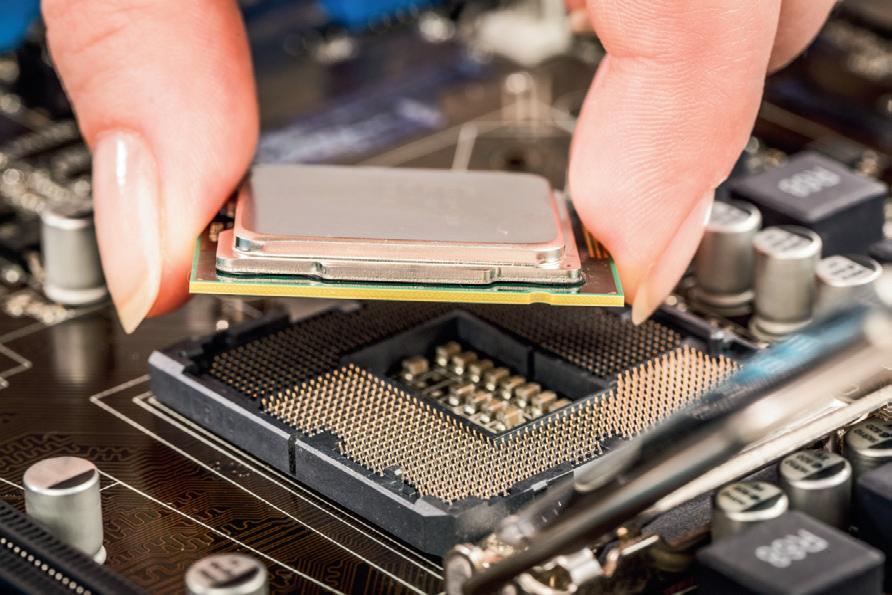
Cybersecurity experts studying memory modules in computers have uncovered a key weakness that has led to worldwide security fixes in AMD computer processors.
The weakness occurs because of ‘BadRAM’ — rogue memory modules that deliberately provide false information to the computer’s processor during start-up.
Processors are present in every computer and are necessary to perform every calculation. The computer’s memory (DRAM) is essential for storing code and data. When a computer boots up, the processor will communicate with DRAM modules to learn size, speed and configuration.
This information is stored on the so-called SPD chip. But by tampering with this chip, the researchers found that attackers were able to bypass the AMD’s security mechanisms put in place to protect sensitive data — particularly data stored in shared cloud environments with pervasive data breaches and insider threats.
In this case, the researchers targeted a security technology called Secure Encrypted Virtualisation (SEV), designed by global computing company AMD. This cutting-edge technology protects privacy and trust in cloud computing by encrypting a virtual machine’s memory and isolating it from advanced attackers.
“We found that using cheap, off-the-shelf equipment, we were able to trick the computer’s processor into allowing access to protected memory,” said Professor David Oswald, School of Computer Science.
The research was carried out by a consortium of experts from KU Leuven, Belgium; the University of Luebeck, Germany; and the University of Birmingham, UK.
It has led to AMD issuing firmware updates to securely validate memory configurations as processors boot up.
The researchers have published a website to explain the weakness and the potential threat posed. They explain that BadRAM makes the computer’s memory module intentionally lie about its size, tricking the CPU into addressing ‘ghost’ memory regions that don’t exist.
This leads to two CPU addresses mapping to the same DRAM location. And through these aliases, attackers can bypass CPU memory protections, exposing sensitive data or causing disruptions.
“We worked with AMD to ensure they were able to adopt appropriate countermeasures so that BadRAM is detected at the point the computer boots up. While it’s good practice to keep your system up to date, most cloud providers will have updated their firmware to include AMD’s countermeasures — so there is no need to worry that your data is not secure!” Oswald said.
Inspired by science fiction technology, the novel antenna is the result of creative cross-disciplinary collaboration across APL.
Electrical engineer Jennifer Hollenbeck said she got the idea from The Expanse series, where alien technology is organic and shape-changing. “I have spent my career working with antennas and wrestling with the constraints imposed by their fixed shape,” she said. “I knew APL had the expertise to create something different.”
In 2019, Hollenbeck reached out to Steven Storck, now chief scientist for additive manufacturing in the Lab’s Research and Exploratory Development Department, who at the time led an Independent Research and Development project to create a promising methodology to additively manufacture shape memory alloys. These unique materials deform at lower temperatures but return to a ‘remembered’ shape when heated and are used in a wide variety of applications, ranging from medical uses such as orthodontic wires, vascular stents and bone implants to actuators for control surfaces in spacecraft.
Mechanical engineer and materials scientist Andy Lennon had used nitinol — a shape memory alloy of nickel and titanium — to create coils that would extend down through a person’s oesophagus to assist with heart imaging. As Lennon and others worked on applications for nitinol, a desire arose to 3D-print complex shapes with it. But that presented a problem: Nitinol and other shape memory alloys conventionally require extensive mechanical processing — known as cold work — to achieve the shape memory effect, and as a result they are typically only available as wire or in thin sheets.
“Doing an extreme amount of cold work would defeat the whole point,” Lennon said. “If you take that complex shape and pass it through a die to stretch it out, you’re back to a wire.”
The APL team initially conducted research to tackle the fundamental challenges associated with scalable additive manufacturing of nitinol components, later applying these techniques to create shape-changing structures that could be deployed in space applications. After extensive experimentation towards the antenna application, the team altered the ratio of nickel and titanium, but the first attempt to create a shape-shifting horn antenna using 3D-printed nitinol fell short. While the antenna did technically expand and contract and change its frequency, it was also rigid and difficult to expand.
“It turned out to be a really complicated design, and it didn’t work as well as I would have liked,” Hollenbeck said.
Undeterred, Hollenbeck and the team submitted a proposal for a Propulsion Grant, one of APL’s internal funding opportunities designed to support the development of revolutionary solutions to critical challenges.
This time, Hollenbeck had a new antenna design in mind. Lennon’s team had been able to 3D-print nitinol with what’s known as two-way shape memory, in which the alloy can be heated and cooled to alternate between two remembered shapes. With critical design and prototyping support from Kyle Sibert, an electrical engineer in APL’s Force Projection Sector, Hollenbeck’s team developed an antenna that was shaped like a flat spiral disk when cool but became a cone spiral when heated.
Heating the spiral proved to be a challenge. The team had to determine how to heat the metal of the antenna enough for it to change shape, but without interfering with the RF properties or burning out the structure. To solve the problem, the team, led by RF and microwave design engineer Michael Sherburne, had to invent a new form of power line.
THE HARD WORK PUT IN BY TEAMS ACROSS APL HAS YIELDED A RADICALLY INNOVATIVE TECHNOLOGY THAT COULD HAVE WIDE-RANGING APPLICATIONS.
“For peak heating, the power line has to handle a lot of current,” Sherburne said. “We had to go back to fundamentals to make this work.”
The final piece of the puzzle was working out how to 3D-print the antenna in a consistent, repeatable fashion. Lennon’s modified nitinol, with its higher concentration of nickel, made it challenging to print at scale.
“We have a lot of experience optimising processing parameters and designs for alloys, but this was a step beyond,” explained additive manufacturing engineer Samuel Gonzalez. “There aren’t many people out there, if anyone, printing this material, so there’s no recipe for how to process it.”
“We made shrapnel in the printer a few times because the antenna is trying to change shape as you’re printing it, due to the heat,” added colleague Mary Daffron. “It wants to peel apart.”
Typically, the team can process an alloy in less than four days, but Daffron and Gonzalez said this particular material took two to four weeks of build time.
Now that they have optimised the processing parameters, they’re already looking for ways to build on their initial success.
“We want to optimise the parameters to work on multiple different machines, to make this more widely applicable, and we know we’ll need to optimise for different variations of the material that might actuate at different temperatures,” Daffron said.
The hard work put in by teams across APL has yielded a radically innovative technology that could have wide-ranging applications, supporting special operators in the field, mobile network telecommunications and even space missions to distant celestial bodies.
APL is pursuing a full patent on behalf of the team for the shapeadaptive antenna technology. The Lab has also provisionally decided to pursue patents for the novel power line for heating the spiral, a method for controlling the antenna, and a method and process for using shape memory alloys to create a phased array antenna.
“The shape-shifting antenna capability that has been demonstrated by this APL team will be a game-changing enabler for many applications and missions requiring RF adaptability in a low-size and -weight configuration,” said APL Chief Engineer Conrad Grant. “This is yet another powerful example of the innovation that occurs at the Laboratory through motivated, highly capable, multidisciplinary teams.”

ST AIoT Craft, a web-based tool from STMicroelectronics, simplifies developing and provisioning node-to-cloud AIoT (Artificial Intelligence of Things) projects that use the machine-learning core (MLC) of ST’s smart MEMS sensors.
The MLC enables decision-tree learning models to run directly in the sensor. Capable of operating autonomously, without host-system involvement, the MLC also enables low latency with low power consumption and handles tasks that require AI skills such as classification and pattern detection.
ST AIoT Craft also integrates all the steps needed for developing and provisioning IoT projects that leverage the MLC for in-sensor AI and offers a secure and user-friendly approach. There is robust cyber protection for data in the cloud and the web-based tool can be accessed online without downloading to desktop. This saves time for users as it requires no installation, and eases collaboration between different team members such as AI specialists and embedded software engineers.
The tool provided for creating decision-tree models includes the AutoML function, which automatically selects optimal attributes, filters and window size for sensor datasets. This framework also trains the decision tree to run on the MLC and generates the configuration file to deploy the trained model. For beginners it is a quick and easy introduction to ST smart sensors that simplifies developing AI applications. In addition, to provision the IoT project, the gateway can be programmed with the Data Sufficiency Module (DSM) tool that filters data points for transmitting to the cloud, to optimise communication and minimise power consumption.
Users can find examples that show how to work with decision trees to build IoT sensor-to-cloud solutions, including fan-coil monitoring, asset tracking, human activity recognition and head gestures. The examples are ready to flash and run for evaluation in ST reference IoT boards such as SensorTile.box Pro, STWIN and STWIN.box. Users can customise these examples to accelerate their own projects, bringing their own data or enhancing available datasets.
ST AIoT Craft is included in the ST Edge AI Suite repository. This contains all software tools, examples and models for developing machine-learning algorithms to deploy on ST edge-AI devices such as STM32 microcontrollers (MCUs), Stellar MCUs and MEMS sensors that contain the MLC or the intelligent sensor processing unit (ISPU).
STMicroelectronics Pty Ltd www.st.com


Jane Nisselson, Columbia Engineering
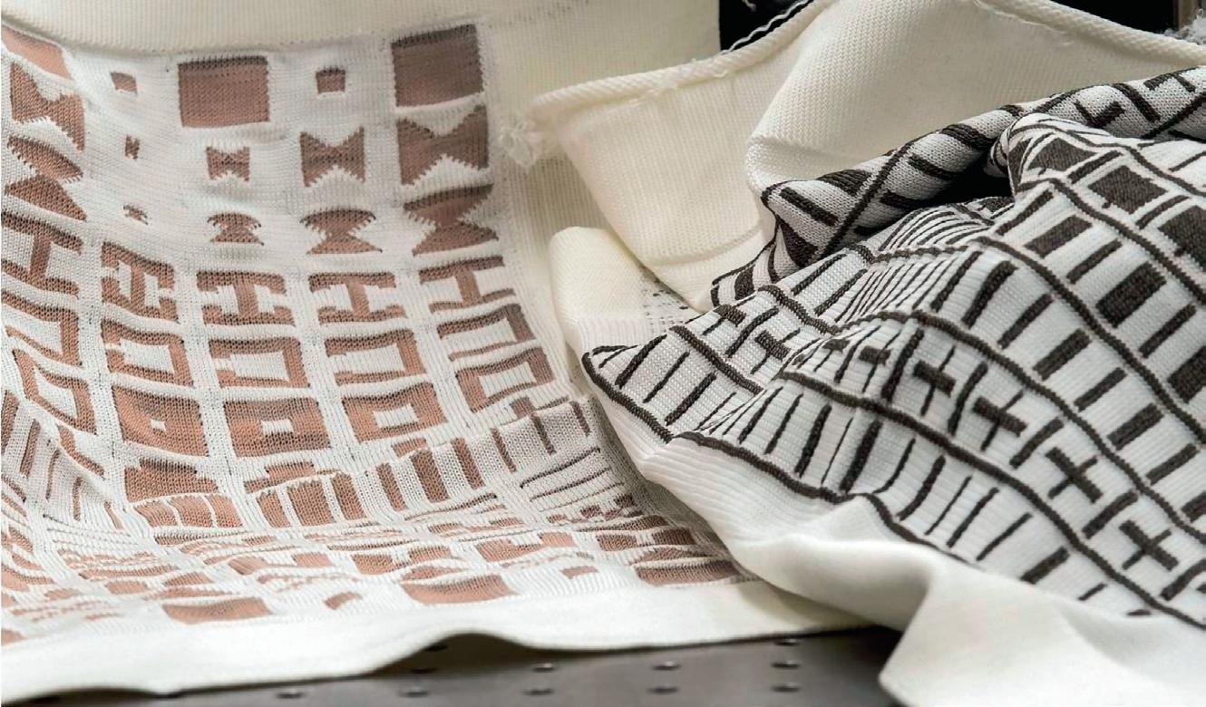
Imagine taking the radio frequency properties of the dish antennas you see on rooftops and knitting them into a wearable garment — a sweater or a blanket that is ultralight, portable, and easy to fold up and stow away.
Not having to use heavy, bulky satellite antennas would make communications much easier for those who live or travel in remote locations — a lightweight, flexible antenna that can send information over long distances would be a useful tool for both the public and private sectors.
A Columbia Engineering team reports that they have used their expertise in metasurfaces — ultrathin optical components that can control the propagation of light — and a low-cost, highly scalable flat-knitting platform to create radio-frequency (RF) communications antennas that are easy to carry and deploy. The study, led by Nanfang Yu, associate professor of applied physics and applied mathematics, was published in Advanced Materials.
Most RF antennas, particularly highly directional array antennas like reflectarrays, are
planar, rigid devices. While these devices will likely always remain state-of-the-art in terms of pure performance metrics, they are often large, heavy and unwieldy and can be expensive to manufacture. Researchers have been investigating ways to produce smaller, more flexible antennas, including inkjet printing or screen-printing directly on textiles, and embroidery. But these techniques are quasi-additive approaches in which a conductive material is added to an existing textile instead of being integrated into the textile during the fabrication process of the textile itself, introducing problems such as delamination, slip or cracking of
the metallic region, as well as issues of production scalability.
Yu’s group realised that what they needed to create was a high-throughput, inexpensive technique that directly integrates flat array antennas onto textiles. So they decided to study knitting and weaving, which, while being the most common approaches for fabricating patterned textiles, have not been explored as a way to produce complex array antennas with engineered electromagnetic responses.
The researchers took a novel approach to fabricating flexible, lightweight centimetre-
Emerson has launched the AVENTICS DS1 dew point sensor, an industrial sensor that is designed to monitor dew point, temperature, humidity levels and quality of compressed air and other non-corrosive gases in real time from one device. The DS1 can help operators detect and mitigate excess moisture in its early stages and prevent moisture-related equipment damage. By optimising air quality in this way, operators can better control processes, extend pneumatic component life and reduce maintenance and unplanned downtime.
The DS1 is designed to provide dew point monitoring that enables manufacturers to continuously track critical values, address excess moisture and prevent its negative effects. For instance, moisture can affect process reliability by corroding components, washing the lubrication out of moving parts and extending switching and reaction times.
The dew point sensor also allows operators to detect changes in air quality in real time with a single device, so they can quickly make necessary adjustments to optimise production and increase overall process reliability.
To support industrial digital transformation strategies, the dew point sensor can be integrated into existing systems, including the AVENTICS Series AS3 and AVENTICS Series 652 air preparation units, and connects to networks via Modbus TCP (PoE). One of the key advantages of an integrated dew point sensor is the ability to place the sensor — and track conditions — close to the process rather than where the compressed air is generated, which can be far from the process itself and have very different conditions. The sensor element is condensation-resistant and provides long-term, drift-proof performance. With fast response time, DS1 measurement values include pressure dewpoint, temperature, relative humidity, absolute humidity, moisture content, moisture content V/V, water vapour partial pressure and atmospheric dew point. The DS1 is also suitable for other non-corrosive gases, including nitrogen, oxygen, argon, helium and sulfur hexafluoride.

Emerson www.emerson.com/au/automation
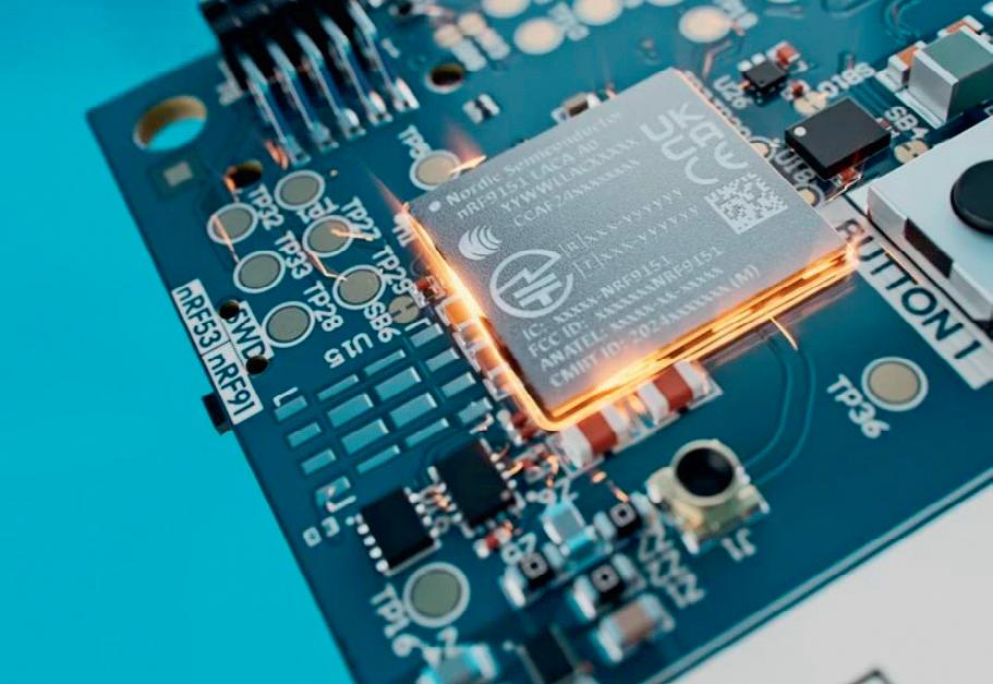
Nordic Semiconductor has launched its latest IoT prototyping platform, the Nordic Thingy:91 X, for LTE-M, NB-IoT, Wi-Fi SSID locationing, DECT NR+ and GNSS applications. The Thingy:91 X simplifies the IoT prototyping process for developers through its suite of onboard features that streamline the development of cellular IoT applications and shorten time-to-market.
Thingy:91 X is a battery-operated device that leverages Nordic’s new nRF9151 system-in-package (SiP). The nRF9151 is a compact cellular IoT SiP for battery-powered and global locationing applications. It features a 20% reduction in footprint compared to Nordic’s nRF9160 and nRF9161 SiPs and is certified for global operation. The nRF9151 SiP also supports LTE-M, NB-IoT, GNSS and DECT NR+ technology.
Thingy:91 X comes equipped with multiple sensors to monitor environmental conditions and track movement. It also features userprogrammable buttons and LEDs, and multiple antennas. A 1350 mAh rechargeable Li-Po battery supervised by Nordic’s nPM1300 power management IC (PMIC) enhances battery life and enables precise fuelgauging. Onomondo and Wireless Logic preloaded SIM cards enable immediate cellular IoT connectivity.
Upon initial setup, the IoT prototyping platform connects to the web interface of nRF Cloud — Nordic’s platform for Cloud services optimised for the company’s wireless solutions — and identifies the Thingy:91 X’s location.
The Thingy:91 X incorporates Nordic’s nRF7002 Wi-Fi companion IC, enabling Wi-Fi service set identifier (SSID) locationing to complement other locationing technologies. The IoT prototyping platform’s capability to support multiple locationing technologies including cellular (single cell [“SCELL”] and multi-cell [“MCELL”] Wi-Fi and GNSS), coupled with nRF Cloud Location Services, enables the developer to balance location accuracy and power consumption. This makes the Thingy:91 X suitable for asset tracking applications.
Thingy:91 X is supported in Nordic’s unified and scalable software development kit, the nRF Connect SDK and Nordic’s Developer Academy. Nordic Semiconductor www.nordicsemi.com
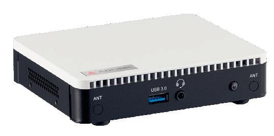
ADLINK Technology Inc. has announced that that its edge visualisation solution, the fanless mini PC EMP-100 series, has received this year’s Taiwan Excellence Award. The award recognises products showcasing innovation, quality and global competitiveness. This highlights ADLINK’s robust R&D capabilities, innovative designs and product quality.
The EMP-100, an industrial-grade fanless mini PC, is an effective digital signage player, suitable for retail spaces, restaurants, shopping centres and manufacturing facilities. Equipped with dual HDMI 2.0 ports, it supports dual 4K ultrahigh-definition displays and features multiple connectivity options and expansion interfaces. ADLINK also offers value-added services to customise port configurations and storage capacity. With standard VESA mounting support, the EMP-100 is a versatile solution tailored to diverse application requirements. ADLINK Technology Inc www.adlinktech.com

Ready for use in forthcoming multi-protocol smart meters that enhance flexibility for handling energy data, the STMicroelectronics ST85MM programmable powerline communication (PLC) modem natively supports field-proven Meters and More and PRIME 1.4 smart grid standards.
The modem is designed to provide a future-proof foundation for advancement, leveraging STMicroelectronics PLC system-on-chip architecture.
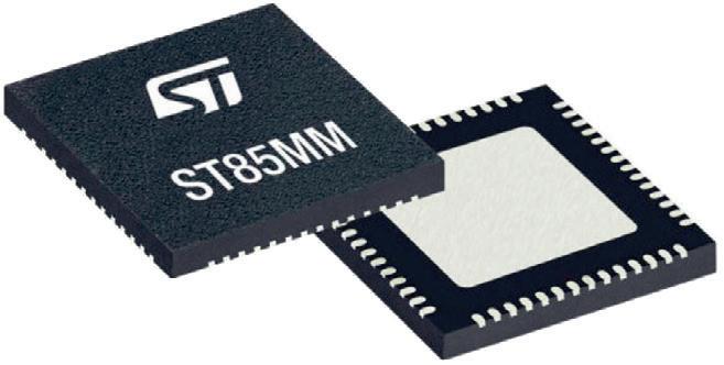
The modem also features programmable DSP and Arm Cortex-M4 core, able to run either Meters and More or PRIME protocols. The modem also integrates the complete PLC analog front end, with a dedicated cryptographic engine for turn-key secure communication. The STLD1 line driver companion IC works with the ST85MM to complete the PLC communication function of the smart-meter design.
On top of the latest protocol capabilities, ST has also announced PRIME 1.4 Hybrid PLC and RF certification for the base node. This leverages the advantages of powerline and wireless connectivity by combining the modem with the S2-LP ultra-low power radio transceiver.
The ST85MM is available now in a 7 x 7 mm QFN56 package.
STMicroelectronics Pty Ltd www.st.com
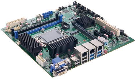
Axiomtek has introduced the MMB541, a Micro ATX motherboard designed for high-performance AI, automation and industrial applications. The motherboard is powered by the LGA1700 socket 14th, 13th and 12th Gen Intel Core i9/i7/i5/i3, Pentium or Celeron processors with Intel H610 chipset. With support for up to 125 W high-performance CPU, it is designed to handle demanding tasks with ease. The industrial motherboard delivers advanced connectivity options with four USB 3.2 Gen1 ports, four USB 2.0 ports and three LAN ports. With support for PCIe x16 for GPU or accelerator cards and PCIe x4 for additional add-on cards, the motherboard is suitable for AI workstations and factory automation setups, providing computational power and high-speed data processing.
The motherboard has dual 288-pin DDR4-3200 non-ECC Long-DIMM for up to 64 GB of system memory. It includes an M.2 Key M 2280/2242 slot for SATA SSD, providing flexible and expanded storage options. The motherboard also offers rich expandability with one PCIe Gen4 x16 slot, two PCIe Gen3 x2 slots from PCH and one 32-bit PCI slot, supporting AI accelerators, vision processing, motion control and various add-on I/O cards.
With triple-display output options— DisplayPort, VGA and DVI-D —the MMB541 is well-suited for multi-screen environments commonly found in factory automation and AI-driven tasks. Featuring a range of I/O interfaces, the motherboard supports four USB 3.2 Gen1, nine USB 2.0, four RS-232, one RS-232/422/485, one RS-232/485, one 2.5GbE LAN and two 1GbE LAN. More functions include watchdog timer and hardware monitoring for CPU/system temperature, voltage detection and smart fan control. Tekdis www.tekdis.com.au


Northwestern University scientists have developed a new protective coating that significantly extends the life of perovskite solar cells, making them more practical for applications outside the lab.
Although perovskite solar cells are more efficient and less expensive than traditional silicon solar cells, perovskite has, until now, been limited by its lack of long-term stability. Typically, perovskite solar cells use an ammonium-based coating layer to enhance efficiency. While effective, ammonium-based layers degrade under environmental stress, including heat and moisture.
Northwestern researchers have now developed a more robust layer — based on amidinium.
In experiments, the new coating was 10 times more resistant to decomposition compared to conventional ammonium-based coatings. Even better: the amidinium-coated cells also tripled the cell’s T90 lifetime — the time it takes for a cell’s efficiency to drop 90% of its initial value when exposed to harsh conditions.
The research has been published in the journal Science
“The field has been working on the stability of perovskite solar cells for a long time,” said Northwestern’s Bin Chen, who co-led the study. “So far, most reports focus on improving the stability of the perovskite material itself, overlooking the protective layers. By improving the protective layer, we were able to enhance the solar cells’ overall performance.”
“This work addresses one of the critical barriers to widespread adoption of perovskite solar cells — stability under real-world conditions,” said Northwestern’s Mercouri Kanatzidis, who co-led the study. “By chemically reinforcing the protective layers, we’ve significantly advanced the durability of these cells without compromising their exceptional efficiency, bringing us closer to a practical, low-cost alternative to silicon-based photovoltaics.”
Chen is a research associate professor of chemistry at Northwestern’s Weinberg College of Arts and Sciences. He co-led the study with Ted Sargent, the Lynn Hopton Davis and Greg Davis Professor Chemistry at Weinberg and professor of electrical and computer engineering at the McCormick School of Engineering, and Kanatzidis, the Charles E. and Emma H. Morrison Professor of Chemistry at Weinberg. Yi Yang, a
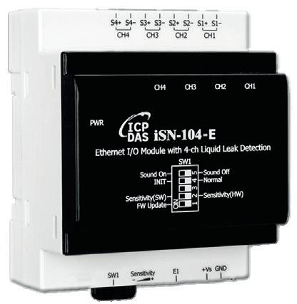
ICP Electronics Australia has launched the ICP DAS iSN-104-E, a 4-channel liquid leak detection module designed for efficient and intelligent liquid leak detection. This Ethernet version device offers a solution for real-time monitoring and alarm control without needing additional conversion modules. The iSN-104-E is also suitable for critical locations like computer room base stations, warehouses, libraries, museums and industrial sites. It also suits applications such as air handling equipment, refrigeration units, liquid containers and pump tanks.
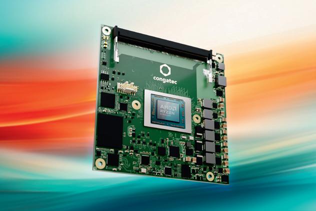
congatec has launched the COM Express Compact Computer-on-Modules with AMD Ryzen Embedded 8000 Series processors. The modules are based on the computing cores of the Ryzen processors featuring up to eight ‘Zen 4’ cores, innovative XDNA NPU and Radeon RDNA 3 graphics.
Key features include water leakage and cable break detection with an audible alarm, a mute button to silence the alarm and five LED indicators to display power and alarm status. The module supports liquid leak detection cables and extended cables up to 500 m, with adjustable sensitivity for precise detection. It is compatible with Modbus TCP/UDP and MQTT protocols, facilitating integration with various monitoring systems for remote alarm and device control.
The module offers redundant power inputs, including PoE and DC input, to facilitate reliable operation. Certified with CE, UKCA, FCC, RoHS and WEEE, it provides high standards of safety and environmental compliance.
The module can also be integrated into existing HMI or SCADA systems, enhancing maintenance in distributed control systems. Applications extend to water pipe leak monitoring in buildings, fire pipes, sewage pipes and domestic water systems, promoting water conservation and safety. It can send out signals and alarms, and integrate with WISE IoT Edge Controllers or TPD/VPD Touch HMIs, further connecting with mobile apps or community systems.
ICP Electronics Australia www.icp-australia.com.au


This makes the conga-TCR8 Type 6 modules suitable for high-volume applications requiring a combination of advanced AI, graphics and computing power. OEMs in medical imaging, test & measurement, AI-supported POS/POI systems and professional gaming can also leverage these longterm available COM Express Compact modules to accelerate innovation. With a broad, scalable TDP range of 15–54 W, these modules are also suitable for upgrading existing designs.
The conga-TCR8 computer-on-modules support up to 128 GB DDR5-5600 memory with error correction code (ECC) for data-intensive and data-critical applications. With the integrated AMD XDNA NPU (16 TOPS) and AMD Radeon RDNA 3 graphics, the modules deliver a combined computing power of up to 39 TOPS. They also support immersive graphics output on up to four displays with resolutions as high as 8K. For fast peripheral connectivity, they offer six PCIe Gen 4 (8 lanes) with PEG x8 Gen 4, three DisplayPort (DP) interfaces, one eDP or LVDS, four USB 3.2 Gen 2 ports, and four USB 2.0 ports.
The modules are also available as applicationready aReady.COMs, with custom pre-installed and validated operating systems like ctrlX OS, Ubuntu and/or RT Linux, optional system consolidation via aReady.VT, and IoT connectivity via aReady.IOT. On request, the modules can be pre-installed with the customer’s application, allowing for simple plug-andplay integration into the finished system. Congatec Australia Pty Ltd www.congatec.com
The SMCBA has secured certification for training Australian electronics manufacturers on IPC/ WHMA-A-620-S, the Space and Military Applications Hardware Addendum to IPC/WHMA-A-620. Design and manufacture of vehicles and equipment for space applications is a strong and growing industry in Australia, but it cannot realise its potential unless it can provide evidence of a capability of achieving the recognized international standards.
To ensure consistency with industry practice, the standard and the addendum are prepared by the IPC in collaboration with the US Wiring Harness Manufacturer’s Association (WHMA) and NASA. While cable and wire harness assemblies are an important part of almost any electronic system there are reasons why an addendum to the basis standard is needed for space applications. In space applications, cables and harness assemblies play a critical role in power distribution, signal transmission, data collection and can even contribute to the structural integrity of the vehicle. There needs to be a higher level of certainty in space applications because even a minor failure could compromise a billion dollar mission. The Space and Military Application Hardware Addendum provides for the survival of the wiring harness under the extreme conditions of vibration and thermal excursions encountered in getting to, and operating in the military and space environments and supplements or replaces the specifically identified requirement of the base IPC/ WHMA-A-620 standard. The certification available through SMCBA is equivalent to NASA-STD-8739.4.
Originally released in 2002, IPC/WHMA-A-620 is the only industry consensus standard for acceptability requirements of cables and wire harness assemblies. Now at revision E (2022) the publications IPC/ WHMA-A-620E and accompanying Addendum IPC/ WHMA-A-620E-S provide the electronics industry with the most comprehensive and current criteria for the performance and acceptance of cable and wire harness assemblies, for all applications. Both Specialist and Trainer certification programs are available. The Space Addendum certification is an optional addition for anyone who achieves IPC/ WHMA-A-620 certification.
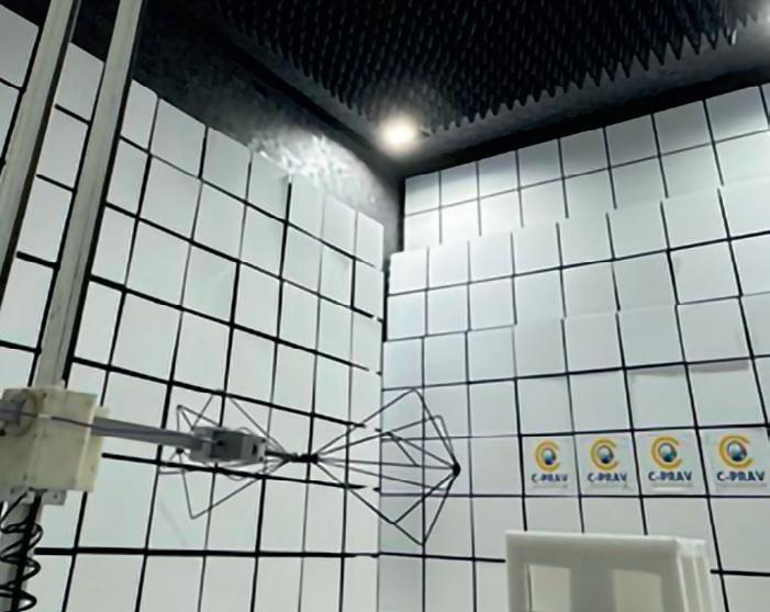
In our efforts to highlight exceptional members within our Association, we are thrilled to showcase C-PRAV Labs & Certi cations, a leading engineering consultancy that specializes in EMC testing & compliance, product safety testing, environmental testing and technical consultancy services for the electronics industry. With a mission to empower innovation while ensuring the highest standards of safety and compliance, C-PRAV exemplifies the values and vision of the SMCBA.


At C-PRAV, it’s recognised that no two challenges are the same. The company delivers bespoke solutions tailored to the unique needs of each client, whether they are startups bringing groundbreaking ideas to life or established manufacturers refining their latest designs.
From initial concept to market launch, C-PRAV offers comprehensive support across the entire product development lifecycle. Their services include:
• Prepare Test Plans: guide you choosing the right standards and precise testing requirements.
• Pre-Compliance Testing: identify and resolve issues before formal certification.
• Full EMC, Safety, and Technology Compliance Testing: Aligned with Australian and International regulations, the test lab is fully accredited by NATA for ISO17025.
• Support with Global Market Access: A unique service in Australia to secure regulatory approvals for Global markets including Australia/New Zealand (RCM), North America (FCC/ ISED/NOM)), Europe (CE & UKCA), South America (ANATEL, etc), Africa (SABS, NRCS, etc) and Asia (VCCI, SDPPI, CCC, IMDA, etc)

The SMCBA is a Licenced IPC Training Centre for the IPC programs - J-STD-001, IPC-A-610, IPC/WHMA-A-620 & 7711/21
• Technical Consultancy: Providing expert guidance on design optimization, regulatory pathways, and troubleshooting to accelerate time-to-market.
• Standards, Regulations, Testing & Certifications (SRTC): Anything to do with Product SRTC, C-PRAV is the go-to team
C-PRAV’s team of dedicated engineers and consultants have more than 3 decades of industry experience and a commitment to staying ahead of technological advancements. Their stateof-the-art laboratory facility in Melbourne is equipped to conduct precise and reliable testing, enabling clients to meet stringent industry regulations with confidence.
“C-PRAV believes in the power of partnership. We work closely with clients to demystify the complexities of compliance and turn obstacles into opportunities”.
“Our collaborative ethos led us to join the SMCBA and we look forward to our sharing insights with the broader electronics community at Electronex and SMCBA Conference later this year.”
“Choose Compliance. Choose Certifications. Choose C-PRAV with Confidence”
C-PRAV Labs and Certifications
P:+61 3 9087 9383
M:+61 412 258 952 praveen@c-prav.com Unit A9, Hallmarc Business Park, 2A, Westall Road, Springvale, Victoria 3171, Australia www.C-PRAV.com
C-PRAV Group: Australia, New Zealand, India, Canada


From the 1960s, high-yielding varieties of wheat spread quickly across Asia, followed by improved strains of rice. At the same time, farmers rapidly increased their use of mineral fertilisers, pesticides and irrigation. The gains were dramatic: over a period of 30 years, the volume of world agricultural production doubled. The ‘Green Revolution’ helped avert major food shortages and promoted rapid economic growth in China, South-East and South Asia.
But the revolution was not without its environmental cost. For example, in some regions, water was being pumped out of the ground for irrigation faster than it could be replenished. Second, widespread use of just a few high-yielding varieties of wheat and rice led to the loss of traditional varieties and increased vulnerability to pests and diseases. Finally, the misuse of fertilisers and pesticides sometimes outweighed their advantages.

Today, more sustainable agriculture techniques are in vogue. Chief among these is ‘precision agriculture’; the technology ensures ideal growth conditions by applying resources like water and fertiliser at the perfect time, significantly improving crop yields. In turn, precision agriculture enables growers to optimise resource use and minimise waste.
Precision agriculture depends on the IoT; the data used to determine the best time to water and feed plants comes from wireless sensors used to monitor soil conditions. One example is Canadian technology company Ginkgo Sustainability’s soil monitoring solution, SoiLiNQ.
The SoiLiNQ solution is made up of multiple SoiLiNQ Sensors powered by Nordic Semiconductor’s nRF52840 SoC and a SoiLiNQ Hub gateway. The SoC not only provides wireless connectivity between sensors and the gateway but also supervises the sensors and collates their data. The gateway is based on Nordic module partner Ezurio’s Sentrius MG100 Gateway2019 and is also supervised by the Nordic SoC. Data is transmitted via the gateway to the Cloud, where users can access it using the SoiLiNQ web application.
“Each SoiLiNQ sensor measures soil moisture, air temperature, humidity and other variables to create a detailed survey of the current conditions,” said Sean Militello, Director of Technology and Innovation at Ginkgo Sustainability. “Together, they provide a clear and accurate picture of environmental health. The solution provides our customers with transparent scientifically sound, actionable business intelligence that lowers their costs,” Militello said.
“Our goal is to allow more companies to enact and support sustainable practices. We also want to help the agriculture industry improve resource usage, crop quality and yields.”
Analysis helps growers better understand their data to make informed decisions. It can also assist in mitigating the impacts of climate change by enabling growers to adapt crop treatment as weather patterns change. In the case of the SoiLiNQ web application, analysis is achieved using methods developed by the company’s academic partners.
Alpha testing of SoiLiNQ, using Ginkgo Sustainability’s third-generation sensors, was able to successfully collect and transmit detailed data about local environments.
Northwestern University

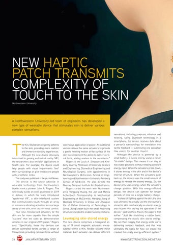
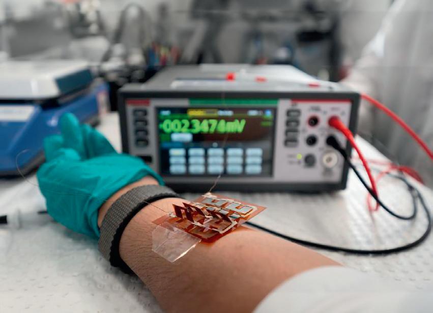
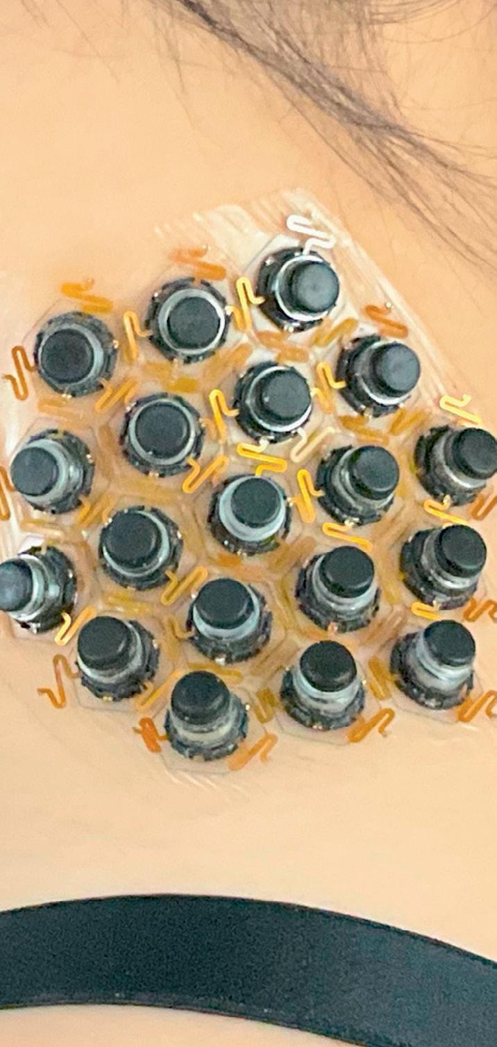
A Northwestern University-led team of engineers has developed a new type of wearable device that stimulates skin to deliver various complex sensations.
The thin, flexible device gently adheres to the skin, providing more realistic and immersive sensory experiences. Although the new device obviously lends itself to gaming and virtual reality (VR), the researchers also envision applications in health care. For example, the device could help people with visual impairments ‘feel’ their surroundings or give feedback to people with prosthetic limbs.
The study was published in the journal Nature
The device is the latest advance in wearable technology from Northwestern bioelectronics pioneer John A. Rogers. The new study builds on work published in 2019 in Nature , in which his team introduced “epidermal VR”, a skin-interfaced system that communicates touch through an array of miniature vibrating actuators across large areas of the skin, with fast wireless control.
“Our new miniaturised actuators for the skin are far more capable than the simple ‘buzzers’ that we used as demonstration vehicles in our original 2019 paper,” Rogers said. “Specifically, these tiny devices can deliver controlled forces across a range of frequencies, providing constant force without
continuous application of power. An additional version allows the same actuators to provide a gentle twisting motion at the surface of the skin to complement the ability to deliver vertical force, adding realism to the sensations.”
Rogers is the Louis A. Simpson and Kimberly Querrey Professor of Materials Science and Engineering, Biomedical Engineering and Neurological Surgery, with appointments in Northwestern’s McCormick School of Engineering and Northwestern University Feinberg School of Medicine. He also directs the Querrey Simpson Institute for Bioelectronics.
Rogers co-led the work with Northwestern’s Yonggang Huang, the Jan and Marcia Achenbach Professorship in Mechanical Engineering at McCormick; Hanqing Jiang of Westlake University in China; and Zhaoqian Xie of Dalian University of Technology in China. Jiang’s team built the small modifying structures needed to enable twisting motions.
The new device comprises a hexagonal array of 19 small magnetic actuators encapsulated within a thin, flexible silicone-mesh material. Each actuator can deliver different
sensations, including pressure, vibration and twisting. Using Bluetooth technology in a smartphone, the device receives data about a person’s surroundings for translation into tactile feedback — substituting one sensation (like vision) for another (touch).
Although the device is powered by a small battery, it saves energy using a clever “bi-stable” design. This means it can stay in two stable positions without needing constant energy input. When the actuators press down, it stores energy in the skin and in the device’s internal structure. When the actuators push back up, the device uses the small amount of energy to release the stored energy. So, the device only uses energy when the actuators change position. With this energy-efficient design, the device can operate for longer periods of time on a single battery charge.
“Instead of fighting against the skin, the idea was ultimately to actually use the energy that’s stored in skin mechanically as elastic energy and recover that during the operation of the device,” said Matthew Flavin, the paper’s first author. “Just like stretching a rubber band, compressing the elastic skin stores energy. We can then reapply that energy while we’re delivering sensory feedback, and that was ultimately the basis for how we create the created this really energy-efficient system.”

At the time of the research, Flavin was a postdoctoral researcher in Rogers’ lab. Now, he is an assistant professor of electrical and computer engineering at the Georgia Institute of Technology.
To identify the optimal design, Huang’s team conducted systematic computational modelling to examine how the device interacts with skin through electromagnetic actuation.
“It is essential that this bi-stability design can be universally applied to all types of human skin. Computational modelling enables precise optimisation, ensuring this capability,” Huang said. “Achieving this solely through trial-and-error experiments would be impossible. Shupeng Li, a co-first author and postdoc in my group, led this modelling effort.”
To test the device, the researchers blindfolded healthy subjects to test their abilities to avoid objects in their path, change foot placement to avoid injury and alter their posture to improve balance.
One experiment involved a subject navigating a path through obstructing objects. As the subject approached an object, the
device delivered feedback in the form of light intensity in its upper right corner. As the person moved nearer to the object, the feedback became more intense, moving closer to the centre of the device.
With only a short period of training, subjects using the device were able to change behaviour in real time. By substituting visual information with mechanical, the device “would operate very similarly to how a white cane would, but it’s integrating more information than someone would be able to get with a more common aid,” Flavin said.
“As one of several application examples, we show that this system can support a basic version of ‘vision’ in the form of haptic patterns delivered to the surface of the skin based on data collected using the 3D imaging function (LiDAR) available on smartphones,” Rogers said. “This sort of ‘sensory substitution’ provides a primitive, but functionally meaningful, sense of one’s surroundings without reliance on eyesight — a capability useful for individuals with vision impairments.”
The title of the study is ‘Bioelastic state recovery for haptic sensory substitution’.
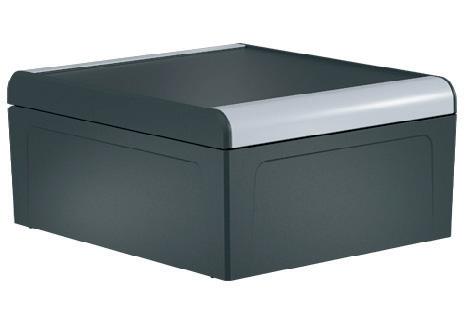
The Metcase premium TECHNOMET desktop instrument enclosures can now be specified without a handle, or with recessed side handles or a tilt/swivel carry handle bar.
The choice of handle options makes these aluminium enclosures readily portable. Applications include medical/wellness, test and measurement equipment, industrial control, peripheral devices and interfaces, switchboxes, communications and laboratory equipment.
TECHNOMET has a modern cohesive design with diecast flush-fit bezels at the front and rear. Snap-on trims hide the fixing screws. The range is available in 11 standard sizes from 225 x 200 x 75 mm to 350 x 320 x 150 mm, including three versions with a sloping front bezel. For 2025, all sizes are now available with the no handle option. For easier portability, three of the larger sizes are available pre-fitted with recessed side handles. All sizes — apart from the sloping-front versions — can also be specified with an adjustable tilt/swivel carry handle bar. It enables TECHNOMET to be positioned at an angle that is suitable for viewing and operation.
TECHNOMET’s internal chassis is pre-punched to accommodate snap-in PCB guides (accessories) in up to nine positions. The base panel is pre-fitted with four M3 PCB mounting pillars. The removable rear panel and anodised front panel (accessory) are both recessed for added protection. All panels have M4 pillars for earthing. Each enclosure is supplied with four non-slip ABS feet.
As standard, TECHNOMET is offered in three colour schemes (depending upon the version selected): anthracite (RAL 7016), light grey (RAL 7035) or a combination of traffic white (RAL 9016) and traffic grey A (RAL 7042). Custom colours can also be specified.
METCASE can supply TECHNOMET fully customised. Services include custom sizes (heights, widths and depths), custom front panels, CNC machining, fixings and inserts, painting and finishing and photo-quality digital printing of legends, logos and graphics.
ADLINK Technology has launched the EMP-100 Mini PC. Measuring just 13 x 10.7 x 2.8 cm, the fanless PC and dual 4K media player is robust and versatile. It includes an Intel Celeron N6210/J6412 processor; IoT connectivity (single GbE LAN and optional Wi-Fi 6/BT 5.2 module); an M.2 2280 Key M for optional storage and Key E for optional WiFi/BT modules; and two HDMI output ports.
The EMP 100 Series was developed to support digital signage with dual 4K UHD display for clear and vibrant content, interactive kiosks, and the development of IoT and AI applications in the smart retail sector — enhancing the customer experience and boosting commercial engagement. The fanless design can operated continuously in a range of temperatures and reduces maintenance.
Typical use cases include digital signage for scheduled marketing campaigns, special offers and discounts; stable system operation at the point of sale with I/O ports for peripherals; and a space-saving mini PC (NUC device) in hospitality settings to drive work efficiency.

The compact design is suited to industrial environments with space restrictions. It can also be integrated into existing infrastructures for edge computing data collection, as well as other applications such as real-time monitoring and status updates for machinery in automated production lines; an IoT gateway connecting sensors and devices on the factory floor to the cloud; and video processing, motion detection and data recording for basic surveillance.
Quectel Wireless Solutions has launched a combo antenna designed to deliver flexibility and choice of network technologies to device designers. The YEMD302L1A is a 3-in-1 combo antenna engineered for connectivity, offering flexible mounting options with magnetic, adhesive, or screw mounts. The antenna supports a broad frequency range for 4G coverage, including 700–960 MHz and 1710–2690 MHz bands. The Wi-Fi frequency coverage ranges from 2400–2500 MHz, 5150–5850 MHz, and 5925–7125 MHz, demonstrating the antenna’s compatibility with the latest Wi-Fi standards up to Wi-Fi 7. This facilitates faster data transfer rates and a stable connection. For navigation, the 1565–1606 MHz GNSS frequency band supports multiple satellite positioning systems, including GPS, BeiDou and GLONASS.
This product meets various international certification standards, including REACH, RoHS, POPs and CE. The product features a UV resistance rating of UL 746c f1, with a durable housing design that provides an IP67 waterproof rating. Suitable for use cases in public safety, high-definition video streaming, smart cities, utilities, fleet management and automotive vehicle tracking, the YEMD302L1A comprises one 4G antenna, one Wi-Fi antenna and one GNSS L1 antenna.
The durability and features of the 3-in-1 combo antenna can be supported by Quectel’s antenna services. Quectel Antenna Services have been developed to help organisations accelerate development by providing con sultation, testing and certification support. Experienced engineers offer bespoke antenna design to enable high performance wireless networking backed by detailed testing and reports to help users achieve certification and network approval.
Quectel www.quectel.com
eight half bridges or single high-side/low-side powering mechanisms such as seat-position adjusters, window lifters, sunroofs, pumps, seatbelt pretensioners and other actuators. The automotive gate driver can also drive resistive loads such as heaters, and the internal circuitry contains a charge pump whose output can control a reverse-battery protection MOSFET.
While the drivers can control both logic-level and standard-level MOSFETs, the extended gate current capability, programmable up to 120 mA, permits driving large numbers of external MOSFETs. Three-stage gate control, which applies the gate signal in three steps, helps to minimise electromagnetic emissions.
Designed to provide each MOSFET’s drainsource voltage (VDS) to an analog-digital converter (ADC), the gate driver leverages indirect current measurement to replace sensing resistors. This ST-patented technique calculates the drain current in each MOSFET by combining the measured VDS with RDS(on) predicted using sensed temperature. The system is calibrated at manufacture to find the nominal RDS(on) values, enabling predictions to be made using the MOSFETs’ resistance-versustemperature curves.
A further feature, also ST-patented, is the programmable multi-failsafe function that turns off bridges individually to protect against faults while allowing unaffected bridges to operate normally. Multi-failsafe detects faults including supply over-voltage, high-side over/under-voltage, thermal warning, charge-pump failure, VDS-monitoring failure, and selectively turns off functions such as diagnostics, watchdog and charge pump depending on fault type.
The L99MH98 is AEC-Q100 qualified and meets ISO 26262 criteria for functional-safety applications up to safety integrity level (ASIL) B.
The automotive gate driver is available now in a VFQFN48L package with wettable flanks and exposed underside cooling pad.
STMicroelectronics Pty Ltd www.st.com
Large-scale production of organic solar cells with high efficiency and minimal environmental impact. This can now be made possible through a new design principle developed at Linköping University.
In the study, published in the journal Nature Energy , the researchers have studied molecule shape and interaction in organic solar cells.
“With electrification and the development of AI, we will probably see a significant increase in the world’s energy needs. That electricity needs to come from environmentally sustainable sources if we are to slow down climate change at the same time,” said Feng Gao, professor of optoelectronics at LiU.
One green energy source in the focus of researchers globally is solar cells. As a complement to traditional silicon solar cells, several different alternative variants are being developed. One of the most promising technologies is based on electrically conductive plastics — organic electronics.
The advantage of organic solar cells is that they are comparatively cheap and easy to manufacture. In addition, they are lightweight and flexible, which means that they could be
placed on windows, indoors or on clothes to power personal electronics. Organic solar cells are already on the market today and their share is expected to increase.
The efficiency of organic solar cells is catching up with traditional solar cells and they
can convert about 20% of the sun’s rays into electricity. The high efficiency is the result of several years of intensive materials research and studies of the interaction between the molecules in the material, the so-called morphology.
Organic solar cells are produced in a physical mixture which is then placed on a substrate and the solvent in the mixture evaporates. However, the chemical solution contains toxic and environmentally hazardous substances.
“To realise mass production of organic solar cells, with printed technologies for example, on a large scale, we need to find methods that don’t use toxins. Otherwise, it’s not good for the environment or for those working in the factories,” said Feng Gao.
His research team has now, together with colleagues in China and the United States, managed to crack the code for producing efficient organic solar cells with several different environmentally friendly solvents.
“To choose the right solvent, it’s important to understand the entire solar cell manufacturing process. This includes knowing the initial structures of the solution, observing the dynamic processes during evaporation and checking the final structure of the solar cell film,” said Rui Zhang, researcher at the Department of Physics, Chemistry and Biology at LiU and lead author of the article published in Nature Energy
What the Linköping researchers have done is map the molecular interaction between the materials transporting the electrons and the solvent itself by using a series of advanced synchrotron X-ray and neutron techniques. Thanks to this, the researchers were then able to develop a design principle that works for many different harmless solvents. In the long run, they hope that even water can act as a solvent.
According to the researchers, understanding the link between morphology and performance in organic solar cells is a major challenge, as they need to investigate the ultra-fast movement of electrons (the charge transport) from the material that releases electrons to the receiving material. Those processes occur within nanoscale structures and at molecular interfaces. According to Feng Gao, the road to environmentally sustainable organic solar cells is now open.
“Thanks to a toxin-free manufacturing method, we now have a much greater chance of commercialising the technology on a larger scale.”
charges and discharges; however, instead of storing energy, this electrochemical process is used to store information.
Once the oxygen atoms leave the tantalum oxide layer, a small region of metallic tantalum is left behind. At the same time, a tantalum oxide layer similarly caps the tantalum metal layer on the opposite side of the barrier. The tantalum and tantalum oxide layers do not mix, similar to oil and water, so these new layers will not revert back to the original state until the voltage is switched.
Depending on the oxygen content of the tantalum oxide, it can act as either an insulator or a conductor — enabling the material to switch between two different voltage states that represent the digital 0s and 1s. Finer control of the oxygen gradient could enable computing inside the memory, with more than 100 resistance states rather than a simple binary. This approach could help reduce power demand.
“There’s a lot of interest in using AI to improve monitoring in these extreme settings, but they require beefy processor chips that run on a lot of power, and a lot of these extreme settings also have strict power budgets,” said Alec Talin, a senior scientist
in the Chemistry, Combustion and Materials Science Department at Sandia National Laboratories and a co-author of the study.
“In-memory computing chips could help process some of that data before it reaches the AI chips and reduce the device’s overall power use.”
The information states can be stored above 1100°F for more than 24 hours. While
that level of heat tolerance is comparable to other materials that have been developed for re-writable, high-temperature memory, the new device comes with other benefits. It can run at lower voltages than some of the leading alternatives — namely, ferroelectric memory and polycrystalline platinum electrode nanogaps — and can provide more analog states for in-memory computing.


Researchers from the City University of Hong Kong have developed a novel metasurface antenna that is capable of simultaneously generating and controlling multiple frequency components through software. The advancement could enhance the efficiency and capabilities of wireless communication systems, particularly for the upcoming 6G networks.
Traditional antennas are typically fixed in their capabilities. To enhance antenna flexibility and control, the researchers experimentally demonstrated a novel antenna concept called a “synthesis moving envelope”. This technology allows antennas to simultaneously generate arbitrary harmonic frequencies and their wave properties to be controlled through software manipulation. The technology has potential applications in next-generation large-capacity and highsecurity information systems, real-time imaging and wireless power transfer. The antenna can simultaneously transmit multiple signals to users in different directions, substantially increasing channel capacity. Professor Chan
Chi-hou, Chair Professor of the Department of Electrical Engineering, said the proposed synthesis approach promotes the metasurfaces’ spectral controllability to a new level.
“The unparalleled frequency controllability, together with its highly straightforward coding strategy (1-bit), sideband-proof and potential for on-chip integration, provides a proposed metasurface antenna that goes beyond existing technologies, offering promising potential in wireless communications, cognitive radar, integrated photonics and quantum science,” said Professor Wu Gengbo from the Department of Electrical Engineering.
The research findings have been published in the journal Nature Communications
Westwick-Farrow Media
A.B.N. 22 152 305 336
Head Office Unit 5, 6-8 Byfield Street, North Ryde
Locked Bag 2226, North Ryde BC NSW 1670 Ph: +61 2 9168 2500
Editor Ashna Mehta wnie@wfmedia.com.au
Publishing Director/MD Janice Williams
Art Director/Production Manager Linda Klobusiak
Art/Production Marija Tutkovska
Circulation Alex Dalland circulation@wfmedia.com.au
Copy Control Ashna Mehta copy@wfmedia.com.au
Advertising Sales
Account Manager
Sandra Romanin – 0414 558 464 sromanin@wfmedia.com.au
Asia
Tim Thompson - 0421 623 958 tthompson@wfmedia.com.au
www.wfmedia.com.au If
Printed and bound by Dynamite Printing Print Post Approved PP100007394 ISSN No. 0728-3873
All