What’s New in Electronics Jan/Feb 2024

Page 1

January/February 2024 Vol.43 No.4 PP100007394

AUTONOMOUS

ELECTROCHEMISTRY ROBOT EXTENDING

EV BATTERY RANGE

RESONATOR

BOOSTS LASER TECH

NEXT-GEN

SEMICONDUCTORS


EDITORIAL COMMENT

CONTENTS

As we settle into a n o t h e r y e a r, it’s only natural to wonder what 2024 will bring to the electronics in-

Robot performs autonomous experiments in the laboratory

dustry in terms of

12

The power of vibrational spectroscopy

good recovery year for the semiconductor

17

More range for EV batteries on the horizon

mid-2024, driven by emerging technologies

21

A micro-ring resonator with big potential

24

Enhancing force detection with electronic ‘stickers’

4

27 30 34

‘Doughnut’ beams reveal secrets of tiny electronics

opportunities and challenges. 2024 has the potential to be a industry, with sales likely to strengthen by like artificial intelligence (AI). The need for green energy solutions — particularly in the electric vehicle (EV) and power grid utility sectors — could also see the demand for batteries rising sharply in 2024. Our first issue of the year is focused on batteries and power supplies. As you will read on page 4, quality control in

Lasers map electrons “going ballistic” in graphene

battery applications is becoming more

Cosmetic ingredient used for battery protection

storage in smaller and smaller formats.

important than ever, as manufacturers strive to provide higher capacity energy The article on page 12 delves into the potential of Raman spectroscopy as a tool to test the electrode composition of new materials before they can be used in commercial products that rely on lithium-ion (Li-ion) batteries, such as mobile phones, laptops and electric vehicles. The EV industry is the current driving force behind the rapid development of batteries, with Li-ion batteries slated to be the most dominant battery technology in 2024. However, the limited availability of key materials (such as lithium and cobalt) has prompted manufacturers to look into developing alternative battery chemistries. The article on page 17 addresses the potential of a new nickel-rich, single-crystal battery technology for electric vehicles that could store more energy per charge and withstand more charging cycles. The magazine also includes articles about micro-ring resonators and the potential of xanthan gum as

Cover image: iStock.com/Olemedia

READ ONLINE!

a protective shield for battery electrodes. I hope you enjoy this issue. Best wishes,

Your copy of What's New in Electronics is available as an online eMag.

Ashna Mehta

www.electronicsonline.net.au/magazine

Editor

WWW.ELECTRONICSONLINE.NET.AU

wnie@wfmedia.com.au


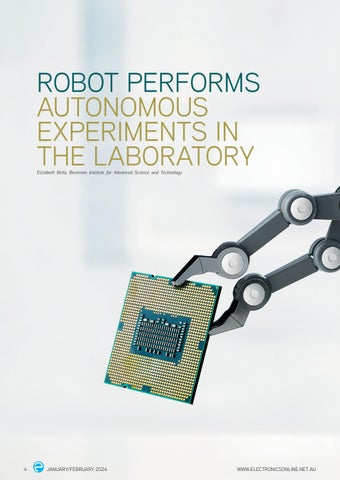
ROBOT PERFORMS AUTONOMOUS EXPERIMENTS IN THE LABORATORY Elizabeth Bello, Beckman Institute for Advanced Science and Technology

4

JANUARY/FEBRUARY 2024

WWW.ELECTRONICSONLINE.NET.AU


ROBOTICS

Researchers at the Beckman Institute for Advanced Science and Technology have developed an automated laboratory robot to run complex electrochemical experiments and analyse data.

W

WWW.ELECTRONICSONLINE.NET.AU

the University of Illinois Urbana-Champaign. The interdisciplinary team was co-led by Rodríguez-López and Charles Schroeder, the James Economy professor in the Department of Materials Science and Engineering and a professor of chemical and biomolecular engineering at UIUC. Their work appears in the journal Device. Electrochemistry is the study of electricity and its relation to chemistry. Chemical reactions release energy that can be converted into electricity — batteries used to power remote controllers or electric vehicles are perfect examples of this phenomenon. In the opposite direction, electricity can also be used to drive chemical reactions. Electrochemistry can provide a green and sustainable alternative to many reactions that would otherwise require the use of harsh chemicals, and it can even drive chemical reactions that convert greenhouse gases such as carbon dioxide into chemicals that are

JANUARY/FEBRUARY 2024

iStock.com/Ivan Bajic

ith affordability and accessibility in mind, the researchers collaboratively created a benchtop robot that rapidly performs electrochemistry. Aptly named the Electrolab, this instrument greatly reduces the effort and time needed for electrochemical studies by automating many basic and repetitive laboratory tasks. The Electrolab can be used to explore energy storage materials and chemical reactions that promote the use of alternative and renewable power sources like solar or wind energy, which are essential to combating climate change. “We hope the Electrolab will allow new discoveries in energy storage while helping us share knowledge and data with other electrochemists — and non-electrochemists! We want them to be able to try things they couldn’t before,” said Joaquín Rodríguez-López, a professor in the Department of Chemistry at

5


ROBOTICS

THE ELECTROL AB IS A C C E L E R AT I N G

THE

D I S COV E RY O F N E W MATERIALS AND WILL ULTIMATELY HELP COMBAT CLIMATE CHANGE.

iStock.com/kynny

useful in other industries. These are relatively simple demonstrations of electrochemistry, but the growing demand to generate and store massive amounts of energy on a much larger scale is currently a prominent challenge. One type of battery, known as a redoxflow battery, is used for grid-level storage and can store and bring power to entire electrical grids. The batteries explored by this collaboration use organic molecules to store energy and can be easily altered or tuned by changing the structure of those molecules. A major drawback of exploring redox-flow battery conditions is that it takes a lot of time and effort to identify a system that works, said Michael Pence, a graduate student of the Rodríguez-López Laboratory and a 2023 Beckman Institute Graduate Fellow. The Electrolab started as an idea between Rodríguez-López and Schroeder based on a collaborative project funded by the Joint Center for Energy Storage Research, an Energy Innovation Hub of the U.S. Department of Energy focused on advancing battery science and technology. Rodríguez-López and Schroeder put together an interdisciplinary team including programmers, engineers and electrochemists. Initially, the idea was to create a microfabricated design, but the team decided to prioritise accessibility and transferability. After establishing the final design of the Electrolab, the research group successfully created and tested an affordable device that is highly adaptable, made from common parts,

6

JANUARY/FEBRUARY 2024

and costs about $1000 to build, which is key for its adoption by laboratories of all sizes. The team is openly sharing construction plans for this instrument, so that all researchers can benefit from it. There are two main components of the Electrolab: hardware and software. The hardware consists of a standard 3D printer frame that was transformed into a solutionhandling robot; microfabricated electrode arrays, or eChips; and electrochemical hardware. The frame allows the robot to move around within a designated area above electrochemical cells to dispense different liquids. The eChips measure electrical current which is necessary for understanding the electrochemical measurements. The software component was created in Python (a free, open-source coding platform) that allows the user to connect with Electrolab to perform experiments. The software allows for fully automated data analysis, visual graphics and plotting. When paired with machine learning, the Electrolab transforms from a robot completing predetermined tasks to a robot that can make decisions about the direction of the experiment while it is happening. Typically, an electrochemist handpicks datasets of interest to move forward, but the Electrolab uses the data it is collecting and analysing in real time to make the next move. In other words, the Electrolab is making this science electro-fast. The bottleneck of electrochemical characterisation is the time required for in-depth

analysis and characterisation of new molecules and solutions. These are tasks like measuring voltages at which battery materials charge and discharge and figuring out the speed of side reactions. There are almost limitless ways to explore and tweak these systems but simply not enough time or bandwidth to explore every option. The Electrolab is accelerating the discovery of new materials and will ultimately help combat climate change. Studying efficient energy conversion and exploring new energy storage materials used in redox-flow batteries would enable alternative energy sources like solar or wind energy to become more practical. At the heart of all that is electrochemistry, Pence said, and that is why Electrolab is so important. In their paper, the research team describe the Electrolab’s function in detail and report the findings of two experiments used to test the accuracy and robustness of their robot. The Electrolab performed more than 200 experiments across multiple conditions, analysed the data and even cleaned up after itself in two hours. This experiment would have taken eight hours for the average electrochemist — depending on their caffeination level. The second experiment tested the Electrolab’s ability to work as a specialist. Programmed to look at a next generation redox-flow battery material in a much more demanding type of experiment to find supporting electrolyte solutions, the Electrolab was modified with smaller, more sensitive electrodes and set to run entirely autonomously. It completed the tasks in less than four hours with no human interference, allowing researchers to work on other projects and reducing background noise that can often be seen in delicate electrochemical analyses. Beyond exploring new battery materials, the Electrolab shows promise for exploring systems where electrochemistry is driving chemical reactions in a green and sustainable manner. As part of his Beckman research, Pence plans to use the Electrolab to screen conditions for oxidation of common biomass by-products, finding ways to transform waste materials into value-added chemicals.

WWW.ELECTRONICSONLINE.NET.AU


NanoEdge AI Studio NanoEdge AI Studio now available for FREE! Free AutoML tool for smarter products

• • • • • • •

Easy-to-use desktop tool to create optimized Machine Learning libraries to address anomaly detection, classification or extrapolation problems Turnkey solution that requires no specific AI or data science skills New algorithms to better predict equipment anomalies and future behaviour High-speed data acquisition and management capabilities Can generate small footprint libraries for all the STM32 portfolio, including the smallest Arm® Cortex®-M0-based MCUs Compatible with all types of sensors Native support for all STM32 development boards

www.st.com/en/development-tools/nanoedgeaistudio STMicroelectronics Suite 703, 247 Coward Street, Mascot, 2020, NSW Australia Tel: +61 2 9158 7201 Email: clifford.shi@st.com

Authorized Distributors ARROW Electronics Australia Pty Ltd - Tel +61 2 9737 4900 Future Electronics - Tel: +61 2 8064 0000 Avnet Electronics (Australia) Ltd - Tel: 1300 791 695


SCIENTISTS LIGHT UP NOVEL BLUE OLED WITH AN AA BATTERY Blue light is vital for light-emitting diodes, lighting applications and large screen displays. However, it can be challenging to develop efficient blue organic light-emitting diodes (OLEDs) due to the high applied voltage required for their function. Conventional blue OLEDs require around 4 V for a luminance of 100 cd/m2; this is higher than the industrial target of 3.7 V — the voltage of lithium-ion batteries typically used in smartphones. Therefore, there is a need to develop novel blue OLEDs that can operate at lower voltages. Now, Associate Professor Seiichiro Izawa from the Tokyo Institute of Technology, in collaboration with researchers from the University of Toyama, Shizuoka University and the Institute for Molecular Science, has developed a novel OLED device with an ultralow voltage of 1.47 V for blue emission and a peak wavelength at 462 nm (2.68 eV). The research findings will be published in Nature Communications. The materials used in this OLED influences its turn-on voltage. The device utilises NDI-HF (2,7-di(9H-fluoren-2-yl) benzo[lmn][3,8]-phenanthroline-1,3,6,8(2H,7H)-tetraone) as the acceptor, 1,2-ADN (9-(naphthalen-1-yl)-10-(naphthalen2-yl)anthracene) as the donor, and TbPe (2,5,8,11-tetra-tertbutylperylene) as the fluorescent dopant. The OLED operates via a mechanism called upconversion (UC), in which holes and electrons are injected into donor (emitter) and acceptor (electron transport) layers, respectively. They recombine at the donor–receptor (D/A) interface to form a charge transfer (CT) state. Izawa said the intermolecular interactions at the D/A interface play a significant role in CT state formation, with stronger interactions yielding superior results. Subsequently, the energy of the CT state is selectively transferred to the low-energy first triplet excited states of the emitter, which results in blue light emission through the formation of a high-energy first singlet excited state by triplettriplet annihilation (TTA). “As the energy of the CT state is much lower than the emitter’s bandgap energy, the UC mechanism with TTA significantly decreases the applied voltage required for exciting the emitter. As a result, this UC-OLED reaches a luminance of 100 cd/m2, equivalent to that of a commercial display, at just 1.97 V,” Izawa said. The researchers have efficiently produced a novel OLED, with blue light emission at an ultralow turn-on voltage, using a typical fluorescent emitter utilised in commercial displays, this marking a step toward meeting the commercial requirements for blue OLEDs. It emphasised the importance of optimising the design of the D/A interface for controlling excitonic processes and holds promise for OLEDs and for organic photovoltaics, along with other organic electronic devices. Lighting up a blue organic LED with a single AA battery.

8

JANUARY/FEBRUARY 2024

iStock.com/D3Damon

CITRUS SOLUTION ENHANCES LI-ION BATTERY RECYCLING EFFICIENCY Used lithium-ion batteries from mobile phones, laptops and a growing number of electric vehicles need to be recycled, but the options for doing so remain limited to mostly burning or chemically dissolving shredded batteries. The current state-of-the-art methods can pose environmental challenges and be difficult to make economical at the industrial scale. The current process recovers few of the battery’s materials and relies on caustic, inorganic acids and hazardous chemicals that may introduce impurities. Recovering metals such as cobalt and lithium could reduce pollution and reliance on foreign sources and choked supply chains. Now, researchers at the US Department of Energy’s Oak Ridge National Laboratory have enhanced approaches that dissolve the battery in a liquid solution in order to reduce the amount of hazardous chemicals used in the process. This simple, efficient and environmentally friendly solution also overcomes the main obstacles presented by previous approaches. The spent batter is soaked in a solution of organic citric acid — which occurs naturally in citrus fruits — dissolved in ethylene glycol, an antifreeze agent commonly used in consumer products like paint and makeup. Citric acid comes from sustainable sources and is much safer to handle than inorganic acids. This green solution produced an efficient separation and recovery process for the metals from the positively charged electrode of the battery, called the cathode. Yaocai Bai, a member of the ORNL research team, said the cathode is the most expensive part of any battery, contributing more than 30% of the cost, because it contains critical materials. “Our approach could reduce the cost of batteries over time,” Bai said. The recycling technique developed at the ORNL laboratory leached nearly 100% of the cobalt and lithium from the cathode without introducing impurities in the system. It also enabled efficient separation of the metal solution from other residues and served a second function by recovering over 96% of the cobalt in a matter of hours, without the typical addition of more chemicals. According to lead researcher Lu Yu, this is the first time one solution system has covered the functions of leaching and recovery. “It was exciting to find that the cobalt would precipitate and settle out without further interference. We were not expecting that,” Yu said. Eliminating the need for extra chemicals reduces costs and avoids creating by-products or secondary wastes. This recycling process could pave the way for greater recovery of battery-critical materials. The leaching performance of citric acid and ethylene glycol has been explored before, but that approach used more acid and a lower temperature, which proved less effective, according to Bai. “We were surprised by how quickly the leaching happened in our solution. With an organic acid, it usually takes 10–12 hours, but this took only one,” Bai said. Conventional solutions using inorganic acid are also slower because they include water, which has a boiling point that limits the temperature of the reaction. WWW.ELECTRONICSONLINE.NET.AU


KEY IMPROVEMENT TO LITHIUM-OXYGEN BATTERIES REVEALED

iStock.com/da-kuk

Lithium-air batteries, sometimes referred to as lithium-oxygen batteries (Li-O2), comprise a lithium metal anode, an organic electrolyte and a porous carbon cathode. During discharge, the oxygen in the surrounding air reacts with lithium at the cathode, releasing energy. Due to their high density (>3500 Wh kg-1), LiO2 batteries could help generate greener sources for energy security. However, advances in the technology have stalled because specially designed carbon cathodes lack certain characteristics, such as abundant active sites where chemical reactions can take place, and space large enough to accommodate the nucleation and growth of discharge products, something necessary to achieve high energy density. Researchers from Tohoku University have developed a porous carbon sheet called a graphene mesosponge sheet (GMS-sheet) that improves the energy density and cycle stability in Li-O2 batteries. Hirotomo Nishihara, co-corresponding author of the paper, said that although the rational design of the porous structure for the carbon cathode is crucial for achieving a high performance, it is also a challenge. “We creatively developed an angstrom-to-millimetre controllable synthesis of freestanding cathodes with minimally stacked graphene free from edge sites,” Nishihara said. To do this, the researchers rationally controlled three synthesis parameters during a chemical vapour deposition (CVD) process: the pelletisation force, the amount of Al2O3 template and the CVD’s duration. Doing so resulted in a series of GMS-sheets with different porosity, amounts of carbon layers and sheet thickness. Wei Yu, co-corresponding author of the paper, said that the specific mass/areal capacities of Li-O2 batteries using GMS-sheets could be controlled by these three synthesis parameters. “By optimising these parameters, we’re excited to achieve impressive energy storage capacities, surpassing the performance of the best carbon cathodes, with more than 6300 milliampere-hours per gram and more than 30.0 milliampere-hours per square centimetre when normalised to the mass and area of GMS-sheets, respectively,” Yu said. The researchers characterised the discharge-charge mechanism using comprehensive in-situ techniques and, in doing so, determined that the hierarchical porous structure of GMS-sheets is vital for enhancing battery performance. Nishihara believes that the GHS-sheet will be a milestone carbon cathode for Li-O2 batteries. “We will continue to promote the practical use of Li-O2 batteries based on our GMS-sheet, and our landscape also covers other metal-gas batteries such as Na-O2, Li-CO2 and Zn-O2 batteries, for which a high-performance carbon cathode is also needed,” Nishihara said. The research findings were published in the journal Advanced Energy Materials.

NOVEL ANTENNA FOR HIGH-SECURITY 6G COMMUNICATIONS

WWW.ELECTRONICSONLINE.NET.AU

The universal metasurface antenna can be used for next-generation, largecapacity, high-security information systems, real-time imaging and wireless power transfer. The antenna’s inherent direction modulation properties also enhance privacy and security, making it suitable for eavesdropper-proof communications. The research findings have been published online in Nature Communications. Professor Wu Gengbo from the Department of Electrical Engineering said the universal metasurface antenna can manipulate information by directly generating the modulated waveform in free space. “We hope that the universal metasurface antenna can work as a simplified information transmitter with low cost, high integration and low power consumption,” Wu said. Professor Chan added that the invention also introduces new features to integrating sensing and communications.

JANUARY/FEBRUARY 2024

iStock.com/bombermoon

A team of researchers from City University of Hong Kong (CityU) has advanced antenna technology by enabling the manipulation of all five fundamental properties of electromagnetic waves through software control. The team, led by Professor Chan Chi-hou, Chair Professor of Electronic Engineering, developed a universal metasurface antenna that allows the independent and simultaneous manipulation of amplitude, phase, frequency, polarisation and direction of electromagnetic radiation. “A universal component capable of manipulating all the fundamental wave properties is the Holy Grail for physicists and engineers,” Chan said. As research on 6G wireless communication systems progresses worldwide, the universal metasurface antenna holds potential for various applications in 6G systems. Its advanced waveform manipulation capabilities and enhanced security features are critical for integrating sensing and communications.

9


AUSSIE RESEARCH HUB TO BOOST 2D MATERIALS MANUFACTURING A new research hub hosted by Monash University at the Faculty of Engineering will foster research and the commercialisation of 2D materials like graphene with a range of applications including in water treatment, batteries, coatings, paints and sensors. The Australian Research Council (ARC) Research Hub for Advanced Manufacturing of 2D Materials (AM2D) was formally opened at an event that showcased the research activities of the Hub and brought together researchers and industry. Featuring high conductivity, strength, and enhanced thermal and optical properties, 2D materials — including graphene — can be used for diverse applications. The new research hub will address this growing demand by enhancing Australia’s graphene and 2D manufacturing capability and supporting the production of high-tech products, such as energy storage devices, advanced anti-corrosion coatings, sensors and water treatment membranes. AM2D Director Professor Mainak Majumder said that there is still a strong investment appetite for research and development into 2D materials and products, adding that graphene’s versatility has spawned many applications that are finding their way to the market. “We are at the tip of this iceberg in this journey as innovative graphene-enhanced products are being designed and existing products are moving up the technology readiness levels (TRL),” Majumder said. Aside from graphene, the research hub will open up new opportunities for next-generation 2D materials. In this family of graphene-like materials, around 100 have reportedly been studied and over 6000 distinct materials are unexplored. “It remains a research area ripe for new discoveries and products. AM2D will build effective partnerships in translating this research into market-ready products,” Majumder said. AM2D has secured $9.4 million in funding over the next five years, including $4.4 million under the Australian Research Council’s Industrial Transformation Research Program. AM2D’s collaborations with universities, including with Monash University, has led to the creation of jobs in manufacturing and high-tech industries. AM2D aims to strengthen these successes and grow the capability of the sector more broadly. Majumder said the hub will take a holistic approach to the development, manufacture and application of 2D materials including how they move across the supply chain. “AM2D is also looking at ways to overcome bottlenecks in sustainably producing and modifying bulk quantities of 2D materials and using machine learning to cost-effectively characterise these materials,” Majumder said. The hub will operate through three major ‘Nodes’ with projects ranging from research on fundamental new tools for 2D materials, smart manufacturing and the environmental impact of the 2D materials sector.

INNOVATIVE BATTERY TECH ACHIEVES MINIMAL VOLTAGE DECAY Lithium-ion batteries are widely used in electronic devices, while lithium- and manganese-rich (LMR) layered oxides are a promising class of cathodes for lithium-ion batteries due to their high capacity. However, their application is hindered by voltage decay. Now, researchers from City University of Hong Kong have addressed the issue by unlocking the potential of LMR cathode materials. The researchers stabilised the honeycomb-like structure within the cathode material, resulting in longer-lasting and more efficient batteries. Their insights could transform the development of highenergy cathode materials. The team’s approach focused on stabilising the honeycomb structure at the atomic level. Incorporating additional transition metal ions into the cathode material helped to reinforce the honeycomb structure, resulting in a voltage decay of 0.02 mV per cycle. Through advanced atomic-scale measurements and calculations, the researchers found that these interlayer transition metal ions act as a ‘cap’ above or below the honeycomb structure, preventing cation migration and maintaining stability. The structure remained intact even at high cut-off voltages and throughout cycling, thereby helping to maintain the batteries’ structural integrity. “Our work has solved the voltage decay problem in the LMR cathode, with a capacity almost two times higher than the widely used cathode materials, ultimately paving the way for more powerful and sustainable energy storage solutions,” Professor Liu Qi said. The researchers will now scale up the manufacturing process for large-scale battery production. The research findings were published in the journal Nature Energy.

10

JANUARY/FEBRUARY 2024

WWW.ELECTRONICSONLINE.NET.AU


ENVIRONMENTALLY FRIENDLY RECIPE FOR EV BATTERY RECYCLING Researchers at Chalmers University of Technology, Sweden, have presented an efficient way to recycle metals from spent electric car batteries. The method reportedly allows recovery of 100% of the aluminium and 98% of the lithium in electric car batteries. The loss of valuable raw materials such as nickel, cobalt and manganese is also reduced, with no harmful chemicals required in the process because the researchers used oxalic acid — an organic acid that can be found in the plant kingdom. “So far, no one has managed to find exactly the right conditions for separating this much lithium using oxalic acid, whilst also removing all the aluminium. Since all batteries contain aluminium, we need to be able to remove it without losing the other metals,” said Léa Rouquette, a PhD student from Chalmers University of Technology. Rouquette and the research leader Martina Petranikova showed how the new method works by using spent car battery cells and, in the fume cupboard, their pulverised contents. This takes the form of a finely ground black powder dissolved in oxalic acid. The exact procedure is unique and requires the fine-tuning of temperature, concentration and time. The researchers also developed a new recipe for using oxalic acid, which can be found in plants such as rhubarb and spinach.

WWW.ELECTRONICSONLINE.NET.AU

“We need alternatives to inorganic chemicals. One of the biggest bottlenecks in today’s processes is removing residual materials like aluminium. This is an innovative method that can offer the recycling industry new alternatives and help solve problems that hinder development,” Petranikova said. The aqueous-based recycling method is called hydrometallurgy. Traditional hydrometallurgy involves the metals in an EV battery being dissolved in an inorganic acid. Then, the ‘impurities’ (such as aluminium and copper) are removed, before the valuable metals such as cobalt, nickel, manganese and lithium are separately recovered. While the amount of residual aluminium and copper is small, it requires several purification steps, with each step likely to cause lithium loss. With the new method, the researchers reversed the order and recovered the lithium and aluminium first, to reduce the waste of valuable metals needed to make new batteries. The latter part of the process, in which the black mixture is filtered, is similar to brewing coffee. While aluminium and lithium end up in the liquid, the other metals are left in the ‘solids’. The next step in the process is to separate aluminium and lithium. Rouquette said that the new method is a promising route for battery recycling that warrants further exploration. “Since the metals have very different properties, we don’t think it’ll be hard to separate them,” Rouquette said.

JANUARY/FEBRUARY 2024

11


XXXXXXXXXXXXXXX

THE POWER OF VIBRATIONAL SPECTROSCOPY Stephan Woods, Sr Manager, Product Management at Thermo Fisher Scientific

Lithium-ion batteries are now virtually ubiquitous, powering everything from cell phones and laptops to vacuum cleaners and electric vehicles.

T

his has led to a constant demand for higher capacity energy storage in ever-smaller formats, driving the development of new materials that can bolster device performance. However, any tweaks to electrode composition must be thoroughly characterised and tested under operating conditions before they can be cleared for use in commercial products, which can be both time consuming and expensive. Additionally, many of the analytical technologies traditionally used in this process require highly skilled personnel to interpret the results, limiting the pool of qualified operators and slowing the rate at which novel battery components can be developed and cleared for manufacture. Fortunately, modern vibrational spectroscopy solutions — such as Raman and Fourier transform infrared (FTIR) instru-

12

JANUARY/FEBRUARY 2024

ments — are becoming increasingly intuitive, allowing a greater number of individuals to quickly become proficient in their operation. This can help to lighten the workload for more experienced team members, as well as speed up analyses for increased plant throughput.

What is Raman?

Raman spectroscopy is a non-destructive technique that relies on the inelastic scattering of incident photons, from ultraviolet through to visible and near-infrared, to determine a sample’s spectral fingerprint. In battery development, it can be used to identify compound constituents, characterise molecular structures, evaluate morphologies, and monitor dynamic processes in cathodes, anodes and electrolytes. Raman imaging takes this concept a step further, allowing users

to make thousands of spectral measurements over an area of interest in quick succession to create a 2D snapshot of a surface, rather than just capturing data from a single point.

In situ inspection

Whether used for single- or multi-point analysis, Raman technologies play an important role in battery R&D, especially for in situ and operando applications, where battery components are studied within an assembled cell under a variety of operating conditions. This allows their performance to be evaluated over entire charge and discharge cycles — assessing everything from ionic dispersion to electrolyte degradation — giving researchers added confidence that their novel designs will stand up to the rigours of everyday use. In situ measurements are particularly helpful in the investigation of lithiation and delithiation, two opposing processes that describe the movement of lithium ions within the battery during charging and discharging cycles. Raman spectral

WWW.ELECTRONICSONLINE.NET.AU


BATTERY RESEARCH

iStock.com/KanawatTH

data is also proving invaluable in the search for alternative carbon allotropes that can be substituted for graphite, helping researchers to determine everything from the number of sheets in a graphene stack to the diameters of single-wall nanotubes, as well as providing vital information about structural defects or disorders. Furthermore, it can be used to study the degree of association of electrolyte ions in solutions and polymers, a factor that directly affects battery performance.

Vibrational versatility

In addition to excelling in the measurement of solids and solutions, Raman is also capable of monitoring gaseous emissions during in situ battery tests, providing an early warning of cell damage prior to any visible signs appearing. This can help to establish a battery’s susceptibility to overheating, overvoltage and mechanical stresses, informing the development of safer, more resilient products. Thanks to the versatility of Raman techniques, they

WWW.ELECTRONICSONLINE.NET.AU

are not limited solely to product development applications, and can also be used to determine the purity of raw materials used in the manufacturing process. Many state-of-the-art instruments feature their own material libraries that facilitate the detection of contaminants, bolstering production QC by minimising the chances of downstream defects.

Infrared insights

A complementary technology often employed alongside Raman in many battery R&D and manufacturing applications is FTIR spectroscopy. Like Raman, FTIR is also a nondestructive technique, making it ideal for examining the behaviour of various regions of battery cells while in situ, aiding the rapid identification of changes that could affect product lifespan and safety. It can also be applied during raw material QC to assess incoming goods, and is widely used for ex situ characterisation of lithium salts, electrolyte formulations and catalytic systems. FTIR

again comes into play during final product QC, helping to confirm that regulatory and stakeholder specifications have been met.

Keeping pace

QC in battery applications is becoming more important than ever, as manufacturers look to squeeze every last drop of efficiency out of existing energy storage solutions, as well as looking ahead to emerging technologies. This has led to vibrational spectroscopy becoming a mainstay of development and production lines around the globe, offering unparalleled insights into the characteristics of novel materials, while also enabling the early detection of impurities and defects during the manufacturing process. With production pressures only likely to increase as time goes by, lithium-ion battery manufacturers must be sure to include Raman and FTIR technologies in their arsenals if they are to produce high-quality products in the vast quantities needed to keep pace with market demands.

JANUARY/FEBRUARY 2024

13


LOW PIN COUNT MICROCONTROLLERS Microchip Technology has released the PIC18-Q20 family of microcontrollers (MCUs). These low pin count MCUs feature up to two I3C peripherals and Multi-Voltage I/O (MVIO). Available in 14- and 20-pin packages as small as 3 x 3 mm, the MCUs are suitable for realtime control, touch sensing and connectivity applications. The MCUs offer configurable peripherals, advanced communication interfaces and easy connection across multiple voltage domains without external components. With I3C functionality and the ability to operate on three independent voltage domains, the MCUs are designed to be used in conjunction with a primary MCU in a larger overall system. This family of MCUs can perform tasks such as processing sensor data, handling low latency interrupts and system status reporting. While the central processing unit (CPU) runs at a different voltage domain, the I3C peripheral operates from 1.0 to 3.6 V. These low-power, small form factor MCUs can be used in a range of space-sensitive applications and markets including automotive, industrial control, computing, consumer, IoT and medical. The MCUs offer high communication rates and lower power consumption, all while maintaining backward compatibility with legacy systems. The I3C and MVIO functionality, combined with Microchip’s configurable Core Independent Peripherals (CIPs), allow for reduced design complexity and a reduction in board space by replacing external level shifters with on-chip multiple voltage domains.

Microchip Technology Hong Kong Limited www.microchip.com

WALL-MOUNTED ENCLOSURES The OKW Gehäusesysteme SMART-PANEL wall-mounted enclosure range offers a variety of features for intelligent systems, designed for the easy control and monitoring of the entire building services system. Whether for wired control, operating centres or radio-connected devices in the smart home; for applications in the IoT/IIoT; in measuring and control engineering or in security technology — the possible uses indoors are diverse. The S114 SMART-PANEL (114 x 114 mm) supplements the existing S84 (84 x 84 mm) and E155 (155 x 84 mm) sizes with a larger, square version. Thus, in addition to installation on standard flush-mounted/cavity wall boxes with an installation opening of 61 mm, installation on larger, international device boxes up to 100 x 100 mm is now also possible. Made of V0 ASA+PC material in traffic white (RAL 9016), the enclosure features a polished bottom part, a top part with a fine surface structure and a screwless enclosure assembly with a snap-in function. The flat, recessed surface for interface integration in the bottom part and the recessed operating area in the top part is designed to protect membrane keyboards, display, and operating elements or touch screens. The SMART-PANEL can also be visually modified according to customer requirements or to adapt the individual design of the unit, eg, by machining for cable openings, interfaces or display cut-outs, printing, decor foils and EMC protection measures. Another interesting option is laser marking: this process is suitable for individual labelling, identifying or marking. In particular, very small machine-readable markings,

INTEGRATED MAGNETIC ENCODERS The Erntec IEP3 series of integrated magnetic encoders can be powered with a supply voltage of both 5 and 3.3 V. This makes it suitable for use in battery-powered applications as well, which are typically operated with 3.3 V. A wide temperature range of -40 to +125°C likewise opens the door for various possible uses. The integrated magnetic encoders are suitable for a range of applications and are characterised by high accuracy in small installation spaces. Application areas include, among others, prosthetics in the field of medical technology; optical applications, such as telescopes, microscopes, lasers or cameras; semiconductor production; or robotics. The ON-axis encoder with 2-pole-sensor magnet is simple in design and robust. Thanks to its modular characteristics, which FAULHABER already established with the IE3 encoder series, the IEP3 encoder represents a platform for various motors from the drive specialist. The new product can be combined with DC motors of the 0816SR, 1016SR and 1024SR series as well as with the stepper motors of the AM0820, AM1020 and AM1524 series. Various options are available for the electrical connection of the encoder, such as PVC or FEP cables, connector options as well as different cable lengths. The integrated magnetic encoders are designed to provide high resolution with up to 10,000 lines per revolution and feature the latest chip technology with accuracy compensation to facilitate positional accuracy and repeatability.

ERNTEC Pty Ltd www.erntec.net

eg, QR codes, data matrix codes, barcodes, consecutive numbering of individual parts and individual texts, can be applied quickly and easily with laser marking. Laser marking is also permanent and thus offers a certain degree of protection against forgery and tampering.

ROLEC OKW Australia New Zealand P/L www.okw.com.au 14

JANUARY/FEBRUARY 2024

WWW.ELECTRONICSONLINE.NET.AU


REMOTE DATA LOGGER MODULE ICP Electronics Australia has launched the ICP DAS DL-110S-E-W, a robust IP67 remote data logger module designed to measure and record illuminance, temperature, humidity and dewpoint data. This compact device is designed for environments that require precise monitoring, with an illuminance measurement range from 0 to 100,000 lux, temperature from -20 to +60°C and humidity from 0 to 100% RH. Equipped with the capacity to store up to 600,000 records complete with date and time stamps, the remote data logger module provides extensive data collection. This data can be accessed in real time, due to the free accompanying software utility for Windows and dedicated iOS and Android apps. These features offer the convenience of data retrieval from any location, as long as the device is network-connected. The remote data logger module also supports key protocols such as DCON, Modbus RTU, Modbus TCP and MQTT. With RS-485 and Ethernet communication interfaces, plus redundant power inputs through PoE and DC input, it is designed to integrate into existing systems. The module’s built-in web server allows for straightforward configuration and firmware updates via Ethernet, eliminating the need for additional software. The DL300 Utility software further simplifies module configuration and real-time data monitoring, offering features like alarm event logging and group management of multiple modules. For greenhouse automation, the DL series can enhance environmental monitoring, supporting cloud management solutions for optimal growth conditions and crop yield. When paired with the WISE-523xM-4GE IIoT smart host and iCAM series network cameras, it extends its capabilities to security, sending instant alerts upon unauthorised access, and supporting cloud-based management for real-time situational awareness.

ICP Electronics Australia Pty Ltd www.icp-australia.com.au

FANLESS COMPUTER Backplane Systems Technology has launched the Neousys Nuvo-9650AWP, a fanless embedded computer that features an IP66 rating for waterproof and dustproof performance. This makes it suitable for demanding defence and military applications, where exposure to harsh environmental conditions is a regular occurrence. Its design features specialised moulded O-rings and a stainless steel and aluminium chassis for protection against dust and water. This is particularly beneficial for use in challenging outdoor or mobile military settings, such as in armoured vehicles or military trucks. Notably, the fanless computer is MIL-STD-810H compliant, enabling it to operate under strenuous conditions. It is equipped with commercial off-the-shelf availability of M12 connectors and essential I/Os, making it a cost-effective solution. The fanless computer includes support for Intel 13th /12th-Gen Core CPUs (up to 24C/32T), up to 64 GB DDR5 4800 SODIMM, and a wide operating temperature range from -25 to 70°C. It also features up to four 802.3at GbE PoE+ ports via M12 X-coded connectors and a USB3.2 Type-C port. The 8–48 VDC input with built-in ignition power control further enhances its applicability in various military and defence scenarios.

Backplane Systems Technology Pty Ltd www.backplane.com.au

1554 IP68 polycarbonate Learn more: www.hammondmfg.com/1554 ausales@hamondmfg.com • 08 8240 2244 WWW.ELECTRONICSONLINE.NET.AU

JANUARY/FEBRUARY 2024

15


Teledyne FLIR has launched the Lepton UW, a micro-thermal camera module

COMPUTERON-MODULES

with an ultra-wide 160-degree field of view (FOV). The new ultra-wide module is

congatec has intro-

suitable for a range of applications including fire detection, process monitoring

duced a range of

and people counting.

COM Express Com-

THERMAL CAMERA

The thermal camera features a usable 120 x 120 thermal resolution and a

pact modules based

scene dynamic range of up to 400°C. Like the entire Lepton family, it also features

on the Intel Core Ultra

thermal sensitivity of <50 mK and the same integrated digital thermal image

processors. Providing a combination of heterogeneous

signal processing capabilities.

compute engines, including CPU, GPU and NPU, the new

The ultra-wide FOV also enables smart building system integrators to utilise

conga-TC700 COM Express Computer-on-Modules are

thermal data within more affordable systems and simplify deployment. Develop-

designed to run demanding AI workloads at the edge.

ers can also leverage the Teledyne FLIR Technical Service Team for assistance

Next to the powerful P-cores and efficient E-cores for

along with online resources — from source codes to licences — to speed up

general computing and the high-performance Intel Arc

the development process.

GPU for graphics-intensive tasks, the integrated neural

The thermal camera also provides a dataset that is not susceptible to over-

processing unit (NPU) called Intel AI Boost contributes

counting through glass while also maintaining personal privacy. When combined with

advanced neural processing capabilities to the overall

building automation software, the Lepton UW can help facility managers optimise

computational architecture. The integrated NPU enables

and automate energy usage, occupant comfort and workspace management.

the efficient integration of advanced artificial intelligence

Teledyne e2v Asia Pacific Limited www.teledyne-e2v.com

workloads at lower system complexity than discrete accelerators. This makes the new Intel Core Ultra processorbased computer-on-modules beneficial for combining high-performance real-time computing with powerful AI capabilities in surgery robots, medical imaging and diagnostic systems, where automatically generated critical findings can support medical personnel. Other applications include situational awareness in industrial applications such as inspection systems, stationary robotic arms, autonomous mobile robots (AMRs) and autonomous guided vehicles (AGVs). The computer-on-modules with Intel Core Ultra proces-

FANLESS PANEL PC ICP Electronics Australia now stocks the iEi AFL3-W15C-ADLP fanless panel PC, powered by 12th Generation Intel Core mobile processors. This provides a seamless performance that meets the demands of contemporary applications. The panel PC’s 10-point capacitive touchscreen comes with an anti-glare and anti-UV coating, making it suitable for outdoor use and environments with bright lighting. This provides clarity and minimises reflection, for an uninterrupted user experience. The panel PC is also suitable for businesses that require remote management. When paired with IEI’s iRIS expansion card, users gain access to IPMI 2.0 remote management capabilities. This allows for a range of network operations including OS installation, power controls and more. The device’s display capabilities include 4K UHD output courtesy of Intel’s 10th generation Ultra HD graphics engine. Connectivity is also futureproofed, with support for Wi-Fi 6E and Bluetooth 5.2 providing fast and efficient wireless connections. Finally, dual full-speed M.2 expansion slots support PCIe Gen4 x4, assuring users of more bandwidth and speed.

ICP Electronics Australia Pty Ltd www.icp-australia.com.au

16

JANUARY/FEBRUARY 2024

sors (code named Meteor Lake) feature 6 P-Cores and up to 8 E-Core support up to 20 threads, making it possible to consolidate distributed devices onto a single platform for the lowest total cost of ownership. The SoC-integrated Intel Arc GPU with up to 8 Xe Cores and up to 128 EUs can handle graphics up to 2x 8K resolution and ultra-fast GPGPU-based vision data (pre)processing. The integrated NPU Intel AI Boost executes machine learning algorithms and AI inferences efficiently. Up to 96 GB DDR SO-DIMM with in-band ECC at 5600 MT/s contributes to power-efficient high data throughput and low latency. The modules are supported by congatec’s OEM solutionfocused high-performance ecosystem, including efficient active and passive cooling solutions and ready-to-use evaluation carrier boards. Customers can order the modules with pre-evaluated real-time hypervisor technology from Real-Time Systems for virtual machine deployments and workload consolidation in edge computing scenarios. The new conga-TC700 COM Express Compact Type 6 modules support the embedded temperature range from 0 to 60°C and are available in a range of standard configurations.

Congatec Australia Pty Ltd www.congatec.com

WWW.ELECTRONICSONLINE.NET.AU


ENERGY STORAGE

MORE RANGE FOR

EV BATTERIES

ON THE HORIZON Oliver Peckham, PNNL

iStock.com/Kulpreya Chaichatpornsuk

A seemingly simple shift in lithium-ion battery manufacturing could pay big dividends, improving electric vehicles’ (EV) ability to store more energy per charge and to withstand more charging cycles, according to new research led by the U.S. Department of Energy’s Pacific Northwest National Laboratory.

WWW.ELECTRONICSONLINE.NET.AU

A

n EV’s mileage depends on the deliverable energy from each of the constituent cells of its battery pack. For lithium-ion cells, both the cell-level energy capacity and the cell cost are bottlenecked by the positive electrode, or cathode. Now that bottleneck might be opening up, thanks to an innovative, cost-effective approach for synthesising single-crystal, high-energy, nickel-rich cathodes that was recently published in Energy Storage Materials.

JANUARY/FEBRUARY 2024

17


ENERGY STORAGE The nickel-rich battery vision

Cathodes for conventional EV batteries use a cocktail of metal oxides — lithium nickel manganese cobalt oxides (LiNi1/3Mn1/3Co1/3O2), abbreviated NMC. When more nickel is incorporated into a cathode, it greatly increases the battery’s ability to store energy, and thus, the range of the EV. As a result, nickel-rich NMC (such as NMC811, where the “8” denotes 80% nickel) is of great interest and importance. However, high-nickel NMC cathodes formed using the standard method are agglomerated into polycrystal structures that are rough and lumpy. This meatball-like texture has its advantages for regular NMC. For NMC811 and beyond, though, the bulbous polycrystal fissures are prone to splitting apart, causing material failure. This renders batteries made using these nickel-rich cathodes susceptible to cracking; they also begin to produce gases and decay faster than cathodes with less nickel.

Challenges of synthesising single-crystal NMC811

One strategy to fix this problem: convert that lumpy, polycrystal NMC into a smooth, single-crystal form by eliminating the problematic boundaries between the crystals — but this conversion is easier said than done. In laboratories, single crystals are grown in environments such as molten salts or hydrothermal reactions that produce smooth crystal surfaces. However, these environ-

ments are not practical for real-world cathode manufacturing, where lower-cost, solid-state methods are preferred. In these more typical solid-state approaches, an NMC cathode is prepared by mixing a metal hydroxide precursor with lithium salt, directly mixing and heating those hydroxides — and producing the agglomerated (lumpily clustered) polycrystal NMC. Using a multiplestep heating process results in micron-sized crystals — but they are still agglomerated, so the undesirable side effects persist.

PNNL’s solution

Led by PNNL battery experts, and in collaboration with Albemarle Corporation, the research team solved these issues by introducing a pre-heating step that changes the structure and chemical properties of the transition metal hydroxide. When the preheated transition metal hydroxide reacts with lithium salt to form the cathode, it creates a uniform single-crystal NMC structure that looks smooth, even under magnification. “The one-step heating process of precursors seems straightforward, but there is a lot of interesting atomic-level phase transition involved to make the single crystal segregation possible,” said Yujing Bi, first author of the paper. “It is also convenient for industry to adopt.” The researchers are now scaling up this single-crystal NMC811 to kilogram level by using lithium salt provided by Albemarle. The scaled single crystals were tested in

realistic 2 Ah lithium-ion pouch cells, using a standard graphite anode to make sure that the battery’s performance was mainly dictated by the new cathode. The first prototype battery equipped with the scaled single crystals was stable, even after 1000 charge and discharge cycles. When the researchers looked at the microscopic structure of the crystals after 1000 cycles, they found no defects and a perfectly aligned electronic structure. “This is an important breakthrough that will allow the highest energy density lithium batteries to be used without degradation,” said Stan Whittingham, a Nobel Laureate and distinguished professor of chemistry at Binghamton University. “In addition, this breakthrough on long-lived batteries will be critical to their use in vehicles that can be tethered to the grid to make it more resilient and to support clean renewable energy sources.” The synthesis method for the single-crystal, nickel-rich cathode is both innovative and cost-efficient. It is also easy to scale up, as it is a drop-in approach that allows cathode manufacturers to use existing production facilities to conveniently produce singlecrystal NMC811 — and even cathodes with more than 80% nickel. “This is a fundamentally new direction for large-scale production of single crystal cathode materials,” said Jie Xiao, the principal investigator of the project and a Battelle Fellow at PNNL. “This work is only part of the cathode technology we are developing at PNNL. In collaboration with Albemarle, we are addressing the scientific challenges in synthesis and scale-up of single crystals and reducing the manufacturing cost starting from raw materials.”

Rapid deployment of EV battery technology

iStock.com/Shutter2U

18

JANUARY/FEBRUARY 2024

In the research phase, set to begin in early 2024, PNNL, teaming up with industry and university partners, will work to realise commercial-scale synthesis and testing with an eye toward production. To accomplish this so quickly, they will use conventional manufacturing equipment and techniques that have been industrially adapted to include PNNL’s scale-up approach (as well as a few other innovations that further reduce costs and waste generation). “During single-crystal synthesis at the kilogram level, we have identified a brand new world full of science and engineering challenges and opportunities. We are excited to apply this new knowledge to accelerate the commercial-scale manufacturing process,” Xiao said. This article was originally published by Pacific Northwest National Laboratory.

WWW.ELECTRONICSONLINE.NET.AU


LoRaWAN MODULES Mouser Electronics, Inc. now stocks the RM126x Series LoRaWAN modules from Laird Connectivity. The modules are based on the Silicon Labs EFR32 SoC and Semtech’s SX126x transceivers, with module/antenna combinations certified to work all over the world in either hosted or host-less modes, providing a global, low-power, long-range solution for challenging LoRaWAN implementations in industrial automation and control, smart agriculture, smart cities, utilities monitoring, transportation, logistics, supply chain, healthcare monitoring and retail. The modules target OEM customers requiring long-range RF performance and minimal power consumption. These small-

POWER MANAGEMENT IC

form-factor PCB modules feature a built-in MHF4 connector. In hosted mode, utilising an external microcontroller, the modules

Element14 has added Nordic Semiconductors’ nPM1300 Power

can be programmed with Laird Connectivity’s AT command set.

Management IC to its semiconductor portfolio to enhance the

In hostless mode, the modules utilise their Cortex-M33 core with

offering for connectivity of devices.

Silicon Labs’ Simplicity Studio to enable users to write their own

The Power Management IC offers a simplified solution to system design by integrating functions that are necessary for embedded

application using C, or take advantage of sample applications and radio certifications offered by Laird Connectivity.

designs into a single, compact package. Its power regulation

The modules also include LoRa Point to Point (LoRa P2P)

provides designers with longer run times and efficient battery

capability, allowing users to create their own private, long-range,

charging, while reducing the number of required components.

point-to-point radio network between two RM126x modules. The

The device integrates many intelligent system management

modules, with an integrated temperature-compensated, crystal

functions, including integrated hard reset functionality for one or

oscillator (TCXO), are designed to perform across industrial tem-

two buttons, battery fuel gauging, a system-level watchdog, power

perature ranges of -40 to +85°C, while the onboard components to

loss warning and recovery from failed boot.

complete a DC-DC converter deliver ultra-low power consumption.

The Power Management IC also includes a 32–800 mA battery

Together with Laird Connectivity’s

charger, two 200 mA buck DCDC regulators, two 100 mA load

FlexPIFA and i-FlexPIFA antennas,

switches (alternatively, a 50 mA LDO), five GPIOs and three LED

available for 868 MHz and 915 MHz

drivers. The device is also USB compatible and can be controlled

frequency bands, the RM126x Series

via an I2C compatible TWI.

modules give developers the flexibility for

Nordic Semiconductor’s nPM1300 Power Management IC is now available from element14 in APAC.

element14 au.element14.com

rapid integration into space-constrained LoRaWAN applications.

Mouser Electronics au.mouser.com

PANEL PC Avalue Technology Inc. has launched the ARC-1037, a rugged panel PC that is designed to withstand harsh environments while delivering high performance. Powered by the Intel Atom Alder Lake-N processor, the panel PC features a 10.4″ 1024x768 LED panel with a 50,000-hour lifespan, for lasting clarity in visual performance. The 5-wire resistive touch screen provides a responsive and intuitive user experience. For added versatility, a USB Type C port with Power Delivery (PD) capabilities (20 V/3 A) supports USB 3.2 (gen2, 5 V/3 A) and DP display functions. The panel PC also features two 2.5 Gigabit Ethernet ports to meet high-speed networking requirements, while the wireless aspect supports highspeed, low-latency technologies such as 5G modules and Wi-Fi 6. Meanwhile, rich I/O design with 2 x COM ports and 2 x USB3.2 gen.2 (10 Gbps) ports facilitates efficient data transfer. Built-in 2 W speakers also enhance audio capabilities for immersive user interaction. The panel PC is resistant to water, dust and shock. Designed to perform in high humidity, high temperature and high vibration conditions, the panel PC is also suitable for industrial automation, rehabilitation equipment and automated kiosks. With an IP65-rated front panel and IP41-rated rear panel, the ARC Series excels in humid and dusty operating environments. The wide temperature range and voltage design mitigate problems caused by temperature fluctuations and voltage instability. Simple mounting mechanisms and panel mounting kits further facilitate use in a variety of applications. Optional optical bonding and coating technologies (such as anti-glare, anti-reflective, anti-UV/IR) provide customised solutions for various display challenges, catering to outdoor displays, mobile devices, vehicle systems, military applications and industrial environments.

Avalue www.avalue.com.tw

WWW.ELECTRONICSONLINE.NET.AU

JANUARY/FEBRUARY 2024

19


RACK CASES The METCASE range of 19″ Combimet rack cases includes the original, open-top, smooth/solid and super-deep versions. Applications include networking, communications, sound/studio systems, laboratory instruments and industrial computers/control technology. These smart aluminium enclosures have a flat, bezel-less front for faster manufacturing in custom sizes. The front panel handles make it easy to pull the cases from racks for inspection and maintenance. The enclosures feature removable top, base and rear panels. The top and base can be specified vented or unvented as standard. Inside there are mounting holes in the base for PCBs and chassis. All panels have M4 earth studs. Combimet is available in heights of 1–6 U and depths of 265 and 365 mm as standard. A 24″/609.6 mm super-deep version offers more space for server rack applications. The open-top Combimet Version T increases ventilation. This version is 2 U/3 U high and 365 mm deep. The smooth/solid-top Combimet has an unvented wraparound cover and removable base and rear panels. Unlike the original Combimet, this version has no visible fixing screws on the top. It is 1 U high and 265/365 mm deep. The enclosure range is available in light grey (RAL 7035) or black (RAL 9005) as standard. The front panel is anodised aluminium. Custom colours are also available on request. The enclosures can be specified in custom heights up to 12 U and also in bespoke widths and depths. Other modification services include custom front panels, CNC machining, fixings and inserts, and photo-quality digital printing of legends, logos and graphics.

ROLEC OKW Australia New Zealand P/L www.metcase.com.au

SMART MODULES Quectel Wireless Solutions has launched the SG520B series of 5G Sub-6 GHz, Wi-Fi 6E and Bluetooth smart modules. The module series has been developed to meet growing needs for smart modules which can support connectivity along with a variety of functions, such as edge computing capability, graphics processing, multimedia and operation of peripherals such as displays, cameras and touch panels. The modules feature a builtin, up-to-date Android operating system and are based on the Qualcomm QCM4490 64-bit octa-core processor from Qualcomm Technologies, Inc. Offering comprehensive cellular connectivity options including worldwide 2G, 3G, 4G and 5G coverage, with LTE Cat 15 and both 5G Release 16 standalone (SA) and 5G non-standalone (NSA), the modules offer 5G and LTE multiple input multiple output (MIMO) technology. The utilisation in MIMO of multiple antennas at the receiver end at the same time and on the same frequency band helps minimise errors and enhance data speed. Further connectivity choices include 2x2 MIMO Wi-Fi 6E, IEEE 802.11 a/b/g/n/ac/ax. and Wi-Fi dual band simultaneous (DBS), with a peak data rate of up to 3.6 Gbps. The smart modules also offer Bluetooth 5.2 and the option of a multi-constellation global navigation satellite system (GNSS) receiver for applications that require fast fixes in any environment. Designed for industrial and consumer applications, typical use cases include smart gateways, customer premise equipment (CPE), Mi-Fi devices, point of sale (POS) terminals, cash registers, dashcam, digital signage and industrial PDAs etc. Available in a 42.5 x 56.5 x 2.95 mm LGA package, the SG520B Series has an operating temperature range of -35 ~ +75°C. The modules also support 1080p H.265/H.264 video encoding and decoding.

Quectel www.quectel.com 20

JANUARY/FEBRUARY 2024

SINGLE BOARD COMPUTER B a c k p l a n e S y ste m s Technology has launched the iBase IB961, a 3.5″ single board computer (SBC) designed for high-performance and versatile applications. Powered by the 13th Gen Intel Core (Raptor Lake-P) processors, including options like the i7-1370PE, i5-1340PE, i5-1335UE and i3-1320PE, this SBC is suitable for handling memory-intensive tasks. The processors feature a hybrid architecture with up to 6 Performance-cores (P-core) and 8 Efficient-cores (E-core). This compact SBC includes M.2 slots (M-Key, E-Key, B-Key) and USB 3.2 ports, thereby enabling high-speed 5G communications and easy integration with various peripherals. Dual Intel LAN support facilitates consistent, high-speed network connections necessary for today’s interconnected world. The SBC also features the integrated graphics of the 13th Gen Intel Core mobile processors. It supports rich visual outputs through dual DisplayPort (1.2), eDP and LVDS, to meet graphic requirements in modern applications. Measuring 102 x 147 mm, the SBC is suitable for environments where space is at a premium. It’s built to withstand the rigors of industrial environments, making it suitable for applications in industrial automation and edge computing.

Backplane Systems Technology Pty Ltd www.backplane.com.au WWW.ELECTRONICSONLINE.NET.AU


SEMICONDUCTORS

EPFL/Alain Herzog

A MICRO-RING

RESONATOR WITH BIG POTENTIAL Michael David Mitchell, EPFL School of Engineering

Researchers from EPFL’s Photonic Systems Laboratory (PHOSL) have developed a chip-scale laser source that enhances the performance of semiconductor lasers while enabling the generation of shorter wavelengths.

T

his pioneering work, led by Professor Camille Brès and postdoctoral researcher Marco Clementi from EPFL’s School of Engineering, represents a significant advance in the field of photonics, with implications for telecommunications, metrology and other high-precision applications. The study, published in the journal Light: Science & Applications, reveals how the researchers, have integrated semiconductor lasers with silicon nitride photonic circuits containing microresonators. This integration results in a hybrid device capable of emitting highly uniform and precise light in both nearinfrared and visible ranges, filling a technological gap that has long challenged the industry. “Semiconductor lasers are ubiquitous in modern technology, found in everything from smartphones to fibre optic communications. However, their potential has been limited by a lack of coherence and the inability to generate visible light efficiently,” Brès said. “Our work not only improves the coherence of these lasers but also shifts their output towards the visible spectrum, opening up new avenues for their use.” Coherence, in this context, refers to the uniformity of the phases of the light waves emitted by the laser. High coherence means the light waves are synchronised, leading to a beam with a very precise colour or frequency. This property is crucial for applications where precision and stability of the laser beam are paramount, such as time keeping and precision sensing.

WWW.ELECTRONICSONLINE.NET.AU

Increased accuracy and improved functionality

The team’s approach involves coupling commercially available semiconductor lasers with a silicon nitride chip. This tiny chip is created with industry-standard, cost-efficient CMOS technology. Thanks to the material’s low-loss properties, there is little to no light that is absorbed or escapes. The light from the semiconductor laser flows through microscopic waveguides into extremely small cavities, where the beam is trapped. These cavities, called micro-ring resonators, are intricately designed to resonate at specific frequencies, selectively amplifying the desired wavelengths while attenuating others, thereby achieving enhanced coherence in the emitted light. The other significant achievement is the hybrid system’s ability to double the frequency of the light coming from the commercial semiconductor laser — enabling a shift from the near-infrared spectrum to the visible light spectrum. The relationship between frequency and wavelength is inversely proportional, meaning that if the frequency is doubled, the wavelength is reduced by half. While the near infrared spectrum is exploited for telecommunications, higher frequencies are essential for building smaller, more efficient devices where shorter wavelengths are needed, such as in atomic clocks and medical devices. These shorter wavelengths are achieved when the trapped light in the cavity undergoes a process called all-optical poling, which

The micro-resonator being activated by a semi-conductor laser.

induces what is known as second-order nonlinearity in the silicon nitride. Nonlinearity in this context means that there is a significant shift, a jump in magnitude, in the light’s behaviour that is not directly proportional to its frequency, arising from its interaction with the material. Silicon nitride does not normally incur this specific second order nonlinear effect, and the team performed an elegant engineering feat to induce it: The system takes advantage of the light’s capacity, when resonating within the cavity, to produce an electromagnetic wave that provokes the nonlinear properties in the material.

An enabling technology for future applications

“We are not just improving existing technology but also pushing the boundaries of what’s possible with semiconductor lasers. By bridging the gap between telecom and visible wavelengths, we’re opening the door to new applications in fields like biomedical imaging and precision timekeeping,” said Marco Clementi, who played a key role in the project. One of the most promising applications of this technology is in metrology, particularly in the development of compact atomic clocks.“This significant advancement lays the groundwork for future technologies, some of which are yet to be conceived,” Clementi said. The team’s understanding of photonics and material science could lead to smaller and lighter devices and lower the energy consumption and production costs of lasers. Their ability to take a fundamental scientific concept and translate it into a practical application using industry standard fabrication underscores the potential of solving complex technological challenges that can lead to unforeseen advances.

JANUARY/FEBRUARY 2024

21


COM EXPRESS MODULE ADLINK Technology Inc. has launched the cExpress-MTL, a compact size COM Express Type 6 module powered by an Intel Core Ultra processor. Featuring Intel modular architecture that integrates CPU, GPU and NPU all-in-one for enhanced

MULTIPROTOCOL MODULES

performance, the module provides up to 8 GPU Xe-cores (128 EUs), an NPU (11pTOPS/8.2eTOPS) and 14 CPU cores at 28 W TDP.

Mouser Electronics, Inc. now stocks the ESP32-C6-

Equipped with hardware-accelerated AV1 encoding and decoding function-

WROOM-1 multiprotocol modules from Espressif

ality, the module is also designed to realise instantaneous media streaming

Systems. These multiprotocol modules offer a

with minimal latency. Along with all PCIe interface upgraded to Gen4 for

turnkey solution for adding wireless connectivity

enhanced data transmission and USB4 support for increased flexibility, the

to applications such as smart homes, industrial

module empowers developers to achieve various graphics- and AI-requiring,

automation, health care and consumer electronics.

battery-powered applications, such as portable medical ultrasound, industrial

The multiprotocol modules feature an embedded

automation, autonomous driving, AI robots and more.

ESP32-C6 system-on-chip (SoC) powered by a

ADLINK is also working to provide I-Pi development kits based on the

160 MHz 32-bit RISC-V single-core micropro-

cExpress-MTL module for out-of-the-box-ready prototyping and referencing.

cessor, with Wi-Fi 6 (802.11ax) and Bluetooth

ADLINK Technology Inc www.adlinktech.com

capability, an integrated 40 MHz crystal oscillator and SPI flash up to 8 MB. The multiprotocol modules support the OFDMA mechanism for both uplink and downlink communications, while also supporting MU-MIMO for downlink traffic,

DUAL OPERATIONAL AMPLIFIER

creating high efficiency and low latency, even

STMicroelectronics’ TSB182 dual operation-

in congested wireless environments.

al amplifier is designed for high-accuracy

These multiprotocol modules also enable cus-

signal conditioning with sensors, including

tomers to build Matter-compliant Wi-Fi end-point

maximum 20 µV input offset voltage, 100

devices and Thread end-point devices, for inter-

nV/°C drift over temperature and 4–36

operability in smart-home devices. The modules

V operating range for medium-voltage

also feature 23 general-purpose input and outputs

applications.

(GPIOs), rich peripherals and on-chip debugging,

In addition to its wide supply-voltage range,

and are offered with an onboard PCB antenna or

the dual operational amplifier is specified from -40

with an external antenna connector.

to 125°C. With maximum offset voltage of 30 µV over the

Also available from Mouser, the Espres-

full temperature range, the op amps provide consistent performance in industrial

sif Systems ESP32-C6-DevKitC-1 is an en-

and automotive environments. The package options include MiniSO-8, which helps

tr y-level development board based on the

designers save board space and target smaller module sizes. AEC-Q100 qualified

ESP32-C6-WROOM-1 module. This development

devices are also available.

board integrates complete Wi-Fi, Bluetooth LE,

The dual operational amplifier also combines fast dynamic response and low

Zigbee and thread functions. Most of the I/O

power consumption, with typical operating current of 650 µA per amplifier. The gain-

pins are broken out to the pin headers on both

bandwidth product (GBW) is 3 MHz, with slew rate of 2 V/µs, for minimal output

sides for easy interfacing. Developers can either

distortion across the frequency range. The input noise voltage of 24 nV/√Hz fulfils

connect peripherals with jumper wires or mount

applications that require high resolution and sensitivity. The devices are also hardened

ESP32-C6-DevKitC-1 on a breadboard. An onboard

against electromagnetic interference for enhanced performance in electrically noisy

USB Type-C port is used for supplying power to

environments. Having rail-to-rail outputs, the dual operational amplifier helps design-

the board, as well as for communication with the

ers utilise the available signal dynamic range and ease circuit design in applications

ESP32-C6 chip. The ESP32-C6-DevKitC-1 features

including sensor interfaces and battery-powered equipment.

a USB-to-UART bridge, pin header, status LEDs,

The TSB182 is in production and available now in MiniSO-8. ST will add a standard

and boot and reset buttons for ease of use.

SO-8 option later in the year.

Mouser Electronics au.mouser.com

STMicroelectronics Pty Ltd www.st.com

22

JANUARY/FEBRUARY 2024

WWW.ELECTRONICSONLINE.NET.AU


DIFFERENTIAL PRESSURE SENSORS Würth Elektronik has expanded its range of WSEN PDUS differential pressure sensors, with two new models that work with an operating voltage of 3.3 V and are therefore compatible with most microcontrollers that support this supply voltage. The sensors are robust and feature an accuracy of up to ±25% FSS tolerance. A sensor version is also available with horizontal nozzles. The new packaging design with horizontal-barbed nozzles enables pneumatic hoses to be connected directly to the sensor nozzles. This eliminates the need for an additional adapter and simplifies the installation process. Equipped with digital I C and analog output interfaces, the sensors deliver 2

fully calibrated pressure data as well as optional temperature data. Different transfer functions from ±1 mbar to +15 bar (±0.0145 to +0.218 PSI) may be selected. The differential pressure sensors, featuring an operating temperature range of -25 to +85°C, can be used in a variety of applications: from HVAC technology to monitoring filter status and detecting gas leaks, through to inhalers. All sensor components in the product range and evaluation boards are available from stock with no minimum order quantities. Würth Elektronik

BENCHTOP IONIZER EXAIR’s Varistat Benchtop Ionizer is designed to neutralise static on charged surfaces in industrial settings. Utilising ionizing technology, the Varistat is a hands-free solution that requires no compressed air and provides a constant stream of particulate-free and staticeliminating air. Easily mounted on benchtops or machines, this static eliminator is manually adjustable and suitable for processes needing comprehensive coverage, like part assembly, web cleaning, printing and more. Once plugged in, the ionizer is designed to provide rapid static decay capable of reducing 1000 V to 100 V in 0.8 s. This product features two replaceable ion emitter points and two 30 PPI foam filters for optimal performance over extended periods, as well as LED lights to signify proper function. Offering customisable options like selectable voltage, variable fan speed and adjustable polarity,

can also design individual

the benchtop ionizer is a comprehensive solution for eliminating

application-specific sen-

static and removing dust, debris and other troublesome particulate.

sor variants on request,

The Varistat is also UL listed and CE compliant. The complete

with customer-specific pressure ranges.

line of Gen4 Static Elimination products includes the Super Ion

Wurth Electronics Australia Pty www.we-online.com

from Compressed Air Australia.

Air Knives, Ion Air Cannons and Ion Air Guns, and are available

Compressed Air Australia Pty Ltd www.caasafety.com.au

ENCLOSURES AND TUNING KNOBS FOR TODAY‘S ELECTRONICS EQUIPMENT! www.okw.com.au

ROLEC OKW Australia New Zealand Pty Ltd Unit 6/29 Coombes Drive, Penrith NSW 2750

WWW.ELECTRONICSONLINE.NET.AU

Phone: +61 2 4722 3388 E-Mail: sales@rolec-okw.com.au

JANUARY/FEBRUARY 2024

23


FLEXIBLE ELECTRONICS

Engineers at the University of California San Diego have developed electronic ‘stickers’ that measure the force exerted by one object upon another.

T

he force stickers are wireless, run without batteries and fit in tight spaces. That makes them versatile for a wide range of applications, from arming robots with a sense of touch to elevating the immersive experience of VR and AR, making biomedical devices smarter, monitoring the safety of industrial equipment, and improving the accuracy and efficiency of inventory management in warehouses. They could be used, for example, in knee implants to measure the forces that implants exert on the joint. Having the ability to sense changes in these forces can be useful for monitoring an implant’s fit, as well as wear and tear. Force stickers could also be placed on the bottom of warehouse packages to measure the weight of their contents, acting as miniature scales for checking inventory. “These force stickers could make technology more intelligent, interactive and intuitive,” said Dinesh Bharadia, professor of electrical and computer engineering at the UC San Diego Jacobs School of Engineering. “Humans, by nature, possess an inherent ability to sense force. This allows us to interact seamlessly with our surroundings and enables clinicians to perform delicate surgical procedures. Providing this force-sensing ability to electronic devices and medical implants could be a game changer for many industries.” The force stickers consist of two main components. One is a tiny capacitor that is just a few millimetres thin and about the size of a grain of rice. The other component is a radiofrequency identification (RFID) sticker, which is a device that functions like a barcode that can be read wirelessly using radio signals. The researchers found a clever way to integrate these two components together so that they can measure the force applied by an object and communicate that information wirelessly to an RFID reader. The capacitor is made of a soft polymer sheet sandwiched between two conductive copper strips. When an external force is applied, the polymer compresses, drawing the copper strips closer together, thereby increasing the electric charge in the capacitor.

24

JANUARY/FEBRUARY 2024

ENHANCING FORCE DETECTION WITH ELECTRONIC ‘STICKERS’ Liezel Labios

This so-called “force sticker” is a thin, flexible electronic device that measures forces between objects in contact. Image credit: David Baillot/UC San Diego Jacobs School of Engineering.

This increase in electric charge as a result of applied force is key, the researchers show, because it creates changes in the signal transmitted by the RFID sticker. An RFID reader remotely measures these changes and translates them into a specific magnitude of applied force. This particular technique of creating changes in RFID signal enables the components within the force sticker to be miniaturised. In comparison, previous

methods to create changes in RFID signal required components that are a thousand times larger in size. Meanwhile, the RFID sticker runs on extremely low power by transmitting radio signals via a technique called backscattering. It takes incoming radio signals from an RFID reader, modifies the signals via electric changes induced by the capacitor, and then reflects the modified signals

WWW.ELECTRONICSONLINE.NET.AU


FLEXIBLE ELECTRONICS

A biocompatible force sticker placed within a model knee joint. David Baillot/UC San Diego Jacobs School of Engineering.

This force sticker, designed for measuring larger forces, is constructed by integrating a tiny force-sensing capacitor (orange) with an RFID sticker (white). David Baillot/UC San Diego Jacobs School of Engineering.

back to the reader, which deciphers and translates them into applied force. As a result, the force sticker runs on essentially no power. “The design is really simple with minimal electronics,” Agrim Gupta, an electrical and computer engineering PhD student in Bharadia’s lab, said. Another design feature is that the capacitor can be customised for various force ranges. By replacing the polymer layer with a softer

WWW.ELECTRONICSONLINE.NET.AU

or stiffer one, the capacitor can be tailored to measure smaller or larger forces, respectively. To demonstrate, the researchers built and tested two types of force stickers. In one sticker, the capacitor was built with a super soft polymer to measure smaller forces, making it suitable for use in experiments in a model knee joint. Placed within the joint, the force sticker accurately measured different applied forces as the researchers pushed

on the joint. The second sticker, in which the capacitor was constructed with a stiffer polymer, was tested in a warehouse packaging experiment. Attached to the underside of a box, it accurately measured the weight of varying quantities of objects placed in the box. In tests, the force stickers were durable, withstanding more than 10,000 force applications, and remained consistently accurate. Additionally, they can be fabricated at low cost, with each sticker amounting to less than $2, the researchers noted. “If we can commercialise this technology, we imagine that in the future a box of them could be sold inexpensively, like a box of Band-Aids,” Gupta said. However, it is worth noting a limitation: these force stickers require a static environment to function effectively and do not perform optimally in highly dynamic surroundings. The researchers are addressing this issue as they seek to further improve the technology. Moving forward, the researchers aim to make the force stickers readable by smartphones, which would eliminate the need for RFID readers.

JANUARY/FEBRUARY 2024

25


EDGE COMPUTING SYSTEM The iBase AGS101T, a new addition to the world of IoT gateway edge

RECEIVER EVALUATION BOARD

computing systems, has a range of robust features and versatile appli-

STMicroelectronics has launched

x6212RE/x6414RE processors. Its compact form factor and ruggedised

the STEVAL-WLC38RX receiver

design make it suitable for demanding industrial environments.

cation potential. This compact, fanless system is powered by Intel Atom

evaluation board containing the

The edge computing system is equipped for 5G readiness. It includes

STWLC38 5W/15W receiver IC to

a dedicated M.2 B-Key 3052 slot that supports a 5G module to facilitate

simplify the development of Qi-

high-speed wireless connectivity essential for IoT applications.

compliant wireless chargers up to

The device also features an

15 W. The receiver evaluation board

array of I/O options, including

can help quickly build and test

2x RS232/422/485, 2x full-size

wireless-charger prototypes. It is used with the STSW-WPSTUDIO

Mini PCI-E, 2x USB 3.1 and

graphical software environment to assist development.

2x USB 2.0 ports. For display

The receiver IC supports the Qi 1.3 15W Extended Power

connectivity, it offers 1x DVI-I and 1x HDMI ports, enhancing its versatility.

Profile (EPP) and 5 W Baseline Power Profile (BPP). It can also

These connectivity options are crucial for various industrial IoT applica-

perform as a 5 W transmitter and allows reverse power transfer

tions that require multiple interfaces.

for device-to-device charging. Integrating a synchronous rectifier

The device is designed to operate in extreme temperatures ranging

and low-dropout (LDO) linear regulator, the IC converts power from

from -20°C to 70°C. This is complemented by its over/under/reverse volt-

the receiver coil to a programmable 4–12 VDC output, with power-

age protection, for stable operation in unpredictable power environments.

transfer efficiency of 85%. ST’s Adaptive Rectifier Configuration

The 9~36 V DC wide-range power input further adds to its robustness,

(ARC) mode, which enhances the usable charging area, extends

making it suitable for diverse industrial settings.

the typical receiver-detection distance by 50% and increases

The edge computing system can also support a 2.5″ SSD and TPM

spatial freedom to position devices for optimal power transfer.

2.0 for enhanced data security. The system’s flexibility in installation, sup-

The STWBC86 Qi 1.2.4 BPP-compatible 5 W transmitter integrates

porting DIN-rail mount and wall mount options, allows it to be integrated

a high-efficiency, low-impedance full-bridge inverter and drivers,

into various industrial scenarios seamlessly.

which provide low power dissipation. The IC controls the energy

Backplane Systems Technology Pty Ltd www.backplane.com.au

transferred through the transmitter coil by adjusting the applied PWM frequency and duty cycle. The IC operates with a wide input-voltage range, which eases use in consumer and industrial products. It is managed with an Arm Cortex-M0+ digital core for efficiency. Integrated non-volatile memory (NVM) permits hosting advanced features and allows protocol evolution by updating firmware. Housed in tiny chip-scale packages, the IC is suitable for compact applications. The STWLC38 wireless power receiver comes in a 2.12 x 3.32 mm WLCSP40, while the STWBC86 transmitter is in a 3.26 x 3.67 mm WLCSP72. Thermal management and electrical protection are built in.

STMicroelectronics Pty Ltd EMC_ad_2019.pdf 1 10/05/2023 10:32:41 AM www.st.com

SINGLE-BOARD COMPUTER The BeagleV-Fire SBC, from BeagleBoard, is powered by Microchip’s PolarFire FCVG484E 5x core RISC-V system-on-chip (SoC) with FPGA fabric. It features robust performance in a compact form factor with versatile I/O interfaces, making it suitable for a range of applications including Internet of Things (IoT) devices, robotics, artificial intelligence and embedded systems. The platform offers opportunities for developers, hobbyists and researchers to explore and experiment with RISC-V technology. The SBC features an RISC-V CPU, with 4x 64-bit RV64GC application cores and 1x 64-bit RV64IMAC monitor/boot core with a performance score of 3.125 CoreMarks/MHz and 1.714 DMIPS/MHz. The device’s FPGA

Accredited testing and global product approvals since 1992

features 23K logic elements (4-input LUT + DFF), 68 Math blocks (18x18 MACC) and 4 SerDes lanes of 12.7 Gbps. Other features of the SBC include a Kingston 16 GB eMMC, 2 GB

Bayswater

LPDDR4 RAM and a microSD card socket. The device also features Gigabit Ethernet, M.2 Key E and a support 2.4 GHz/5 GHz Wi-Fi module to facilitate networking. Add-on board expansions include a high-speed SYZYGY interface, a 22-pin CSI connector and BeagleBone-compatible 92-pin cape header pins. The product follows the principles of open-source hardware, enabling users to access and modify the board’s design and firmware. It also comes with Ubuntu pre-installed.

element14 au.element14.com 26

JANUARY/FEBRUARY 2024

WWW.ELECTRONICSONLINE.NET.AU


NANOELECTRONICS

iStock.com/AeganBlue

‘DOUGHNUT’ BEAMS REVEAL SECRETS OF TINY ELECTRONICS University of Colorado Boulder

In a new study, researchers at CU Boulder have used doughnut-shaped beams of light to take detailed images of objects too tiny to view with traditional microscopes.

WWW.ELECTRONICSONLINE.NET.AU

T

he new technique could help scientists improve the inner workings of a range of ‘nanoelectronics’, including the miniature semiconductors in computer chips. The discovery was highlighted in a special issue of Optics & Photonics News called Optics in 2023. The research is the latest advance in the field of ptychography, a difficult to pronounce (the “p” is silent) but powerful technique for viewing very small things. Unlike traditional microscopes, ptychography tools don’t directly view small objects. Instead, they shine lasers at a target, then measure how the light scatters away — a bit like the microscopic equivalent of making shadow puppets on a wall.

So far, the approach has worked remarkably well, with one major exception, said study senior author and Distinguished Professor of physics Margaret Murnane. “Until recently, it has completely failed for highly periodic samples, or objects with a regularly repeating pattern,” said Murnane, fellow at JILA, a joint research institute of CU Boulder and the National Institute of Standards and Technology (NIST). “It’s a problem because that includes a lot of nanoelectronics. She noted that many important technologies like some semiconductors are made up of atoms like silicon or carbon joined together in regular patterns like a small grid or mesh. To

JANUARY/FEBRUARY 2024

27


NANOELECTRONICS

Doughnut-shaped beams of light scatter away from two incredibly small structures with different repeating patterns. Wang, et al., 2023, “Optica”

date, those structures have proved tricky for scientists to view up close using ptychography. In the new study, however, Murnane and her colleagues came up with a solution. Instead of using traditional lasers in their microscopes, they produced beams of extreme ultraviolet light in the shape of doughnuts. The team’s novel approach can collect accurate images of tiny and delicate structures that are roughly 10 to 100 nanometres in size, or many times smaller than a millionth of an inch. In the future, the researchers expect to zoom in to view even smaller structures. The doughnut, or optical angular momentum, beams also won’t harm tiny electronics in the process — as some existing imaging tools, like electron microscopes, sometimes can. “In the future, this method could be used to inspect the polymers used to make and print semiconductors for defects, without damaging those structures in the process,” Murnane said. Bin Wang and Nathan Brooks, who earned their doctoral degrees from JILA in 2023, were first authors of the new study.

Pushing the limits of microscopes

The research, Murnane said, pushes the fundamental limits of microscopes: because of the physics of light, imaging tools using lenses can only see the world down to a resolution of about 200 nanometres — which isn’t accurate enough to capture many of

28

JANUARY/FEBRUARY 2024

the viruses, for example, that infect humans. Scientists can freeze and kill viruses to view them with powerful cryo-electron microscopes, but can’t yet capture these pathogens in action and in real time. Ptychography, which was pioneered in the mid-2000s, could help researchers push past that limit. To understand how, go back to those shadow puppets. Imagine that scientists want to collect a ptychographic image of a very small structure, perhaps letters spelling out “CU”. To do that, they first zap a laser beam at the letters, scanning them multiple times. When the light hits the “C” and the “U” (in this case, the puppets), the beam will break apart and scatter, producing a complex pattern (the shadows). Employing sensitive detectors, scientists record those patterns, then analyse them with a series of mathematical equations. With enough time, Murnane explained, they recreate the shape of their puppets entirely from the shadows they cast. “Instead of using a lens to retrieve the image, we use algorithms,” Murnane said. She and her colleagues have previously used such an approach to view submicroscopic shapes like letters or stars. But the approach won’t work with repeating structures like those silicon or carbon grids. If you shine a regular laser beam on a semiconductor with such regularity, for example, it will often produce a scatter pattern that is incredibly uniform — ptychographic algorithms

struggle to make sense of patterns that don’t have much variation in them. The problem has left physicists scratching their heads for close to a decade.

Doughnut microscopy

In the new study, however, Murnane and her colleagues decided to try something different. They didn’t make their shadow puppets using regular lasers. Instead, they generated beams of extreme ultraviolet light, then employed a device called a spiral phase plate to twist those beams into the shape of a corkscrew, or vortex. (When such a vortex of light shines on a flat surface, it makes a shape like a doughnut.) The doughnut beams didn’t have pink glaze or sprinkles, but they did the trick. The team discovered that when these types of beams bounced off repeating structures, they created much more complex shadow puppets than regular lasers. To test out the new approach, the researchers created a mesh of carbon atoms with a tiny snap in one of the links. The group was able to spot that defect with precision not seen in other ptychographic tools. “If you tried to image the same thing in a scanning electron microscope, you would damage it even further,” Murnane said. Moving forward, her team wants to make their doughnut strategy even more accurate, allowing them to view smaller and even more fragile objects — including, one day, the workings of living, biological cells.

WWW.ELECTRONICSONLINE.NET.AU


MODULES congatec has launched its latest SMARC Module 2.1 Computer-on-Modules, based on Texas Instruments Jacinto 7 TDA4x or DRA8x processors. These new industrial-grade computer-on-modules are suitable for high-performance AI edge applications with an ultra-low power (ULP) envelope featuring dual Arm Cortex-A72 processors, AI accelerators and 3D graphics. The modules consume 5 to 10 W and target industrial mobile machinery that requires 2d/3d camera, radar and lidar-based near-field analytics, such as automated guided vehicles (AGVs) and autonomous mobile robots (AMRs), as well as applications in construction and agricultural machinery. They are also suitable for any vision-focused industrial automation or medical solutions that require energy-efficient AI processing at the edge. The modules come with two MIPI CSI camera inputs. The TDA4x processor-based conga-STDA4 adds an image signal processor (ISP), vision accelerators and pre-trained AI models from the TI Model Zoo. Additionally, it includes a Robotic SDK for enhanced functionality. The DRA8x variants offer a cost-efficient option without vision processing accelerators. Designed to withstand harsh industrial environments, both high-throughput module variants support the extended temperature range from -40 to +85°C, as well as Time-Sensitive Networking (TSN), and cybersecurity measures.

Congatec Australia Pty Ltd www.congatec.com

GPU EDGE SYSTEM The eBOX671B, a fanless edge computing system from Axiomtek, facilitates data transfer with 2.5GbE LAN ports, cellular 5G module and Wi-Fi 6 module support for edge computing in industrial automation. With its compatibility with MXM 3.1 Type A GPU cards, the fanless edge system can accommodate up to five display outputs. Designed to operate in industrial environments, the IP40-rated embedded system features an operating temperature of -40 to +65°C, 3 Grms vibration resistance, and a 9 to 36 VDC power input. The fanless edge system is suitable for various industrial automation applications such as edge controllers, embedded controllers, machine vision, OT servers, robotics and more. The device is powered by the 13th/12th gen Intel Core i9/i7/i5/i3 and Celeron processors with Intel R680E chipset (codename: Alder Lake S). The eBOX671B comes with two 262-pin DDR5-4800 SO-DIMM slots with up to 64 GB of system memory. Two 2.5″ SATA HDD/SSD (RAID 0,1 supported) drive bays, one NVMe through M.2 Key M 2280 slot and one mSATA are available for extensive storage needs. Up to five display outputs are enabled via two HDMI 1.4b, one DisplayPort 1.4a, and two DisplayPort 1.4a via an optional MXM module kit. The fanless edge system also offers great expansion interfaces with one full-size PCI Express Mini Card slot, one M.2 Key M 2280 socket for storage, one M.2 Key E 2230 socket for Wi-Fi 6E, and one M.2 Key B 3052 socket for 5G connectivity. Plus, one front-access SIM slot with cover (through M.2 Key B) and one internal SIM slot for PCIe Mini Card slot are available.

Tekdis www.tekdis.com.au

MOTHERBOARD ADLINK Technology Inc. has launched the IMB-M47 industrial ATX motherboard for 12th and 13th Gen Intel Core i9/i7/i5/i3 processors. The motherboard is designed to provide highperformance computing power, with multiple I/O and expansion ports, including three simultaneous independent displays, USB 3.2 Gen2x2 (20 Gb/s), 3x 2.5GbE, multi-M.2 Key M, TPM 2.0, and PCIe 5.0 high-performance add-on cards for complex Edge AIoT processing tasks in industrial automation, machine vision, factory automation and logistics. The industrial ATX motherboard supports 12th and 13th Gen Intel Core processors that utilise a high-performance hybrid architecture with up to 16 E-cores (Efficient-cores) for multi-threaded background task management and multitasking, and up to eight P-cores (Performance-cores) for demanding single-threaded work such as graphics and video rendering. The processors speed up edge applications that benefit from faster memory performance with faster DDR5 memory. The motherboard provides support for ADLINK’s range of prevalidated PCI/PCIe expansion cards for motion, vision and I/O that provide fast and convenient deployment for real-time graphics processing in automation applications. The IMB-M47 utilises 7x PCIe slots (PCIe 5.0 single x16 or dual x8, 2x PCIe 4.0 x4, and 3x PCIe 3.0 x1), DDR5 (up to 128 GB and 4800 MHz), 2.5 GbE LAN with security and manageability features, and AI enablement to help boost productivity and fuel future innovation in Edge AI applications.

ADLINK Technology Inc www.adlinktech.com WWW.ELECTRONICSONLINE.NET.AU

JANUARY/FEBRUARY 2024

29


BALLISTIC TRANSFER

LASERS MAP ELECTRONS “GOING BALLISTIC” IN GRAPHENE 30

JANUARY/FEBRUARY 2024

WWW.ELECTRONICSONLINE.NET.AU


BALLISTIC TRANSFER

Research appearing in ACS Nano, a journal about nanoscience and nanotechnology, has reve a l e d t h e b a l l i s t i c movement of electrons in graphene in real time.

iStock.com/Sodsai SC

WWW.ELECTRONICSONLINE.NET.AU

T

he observations, made at the University of Kansas’s Ultrafast Laser Lab, could lead to breakthroughs in governing electrons in semiconductors, fundamental components in most information and energy technology. Lead author Ryan Scott said that generally, electron movement is interrupted by collisions with other particles in solids. “These collisions are rather frequent — about 10 to 100 billion times per second. They slow down the electrons, cause energy loss and generate unwanted heat. Without collisions, an electron would move uninterrupted within a solid, similar to cars on a freeway or ballistic missiles through air. We refer to this as ‘ballistic transport’,” Scott said. Scott performed the lab experiments under the mentorship of Hui Zhao, professor of physics & astronomy at KU. They were joined in the work by former KU doctoral student Pavel Valencia-Acuna. Zhao said electronic devices utilising ballistic transport could potentially be faster, more powerful and more energy efficient. “Current electronic devices, such as computers and phones, utilise silicon-based field-effect transistors. In such devices, electrons can only drift with a speed on the order of centimetres per second due to the frequent collisions they encounter. The ballistic transport of electrons in graphene can be utilised in devices with fast speed and low energy consumption,” Zhao said. The researchers observed the ballistic movement in graphene, a promising material for next-generation electronic devices. Graphene is made of a single layer of carbon atoms forming a hexagonal lattice structure — somewhat like a soccer net. “Electrons in graphene move as if their ‘effective’ mass is zero, making them more likely to avoid collisions and move ballistically,” Scott said. “Previous electrical experiments, by studying electrical currents produced by voltages under various conditions, have revealed signs of ballistic transport. However, these techniques aren’t fast enough to trace the electrons as they move.” According to the researchers, electrons in graphene (or any other semiconductor) are like students sitting in a full classroom, who can’t freely move around because the desks are full. The laser light can free electrons to momentarily vacate a desk, or ‘hole’ as physicists call them. “Light can provide energy to an electron to liberate it so that it can move freely. This is similar to allowing a student to stand up and walk away from their seat. However, unlike a charge-neutral student,

an electron is negatively charged. Once the electron has left its ‘seat’, the seat becomes positively charged and quickly drags the electron back, resulting in no more mobile electrons — like the student sitting back down,” Zhao said. Because of this effect, the super-light electrons in graphene can only stay mobile for about one-trillionth of a second before falling back to their seats. This short time presents a challenge to observing the movement of the electrons. To address this problem, the researchers designed and fabricated a four-layer artificial structure with two graphene layers separated by two other single-layer materials, molybdenum disulphide and molybdenum diselenide. “With this strategy, we were able to guide the electrons to one graphene layer while keeping their ‘seats’ in the other graphene layer. Separating them with two layers of molecules, with a total thickness of just 1.5 nanometres, forces the electrons to stay mobile for about 50-trillionths of a second, long enough for the researchers, equipped with lasers as fast as 0.1-trillionth of a second, to study how they move,” Scott said. The researchers used a tightly focused laser spot to liberate some electrons in their sample. They traced these electrons by mapping out the “reflectance” of the sample, or the percentage of light they reflect. “We see most objects because they reflect light to our eyes,” Scott said. “Brighter objects have larger reflectance. On the other hand, dark objects absorb light, which is why dark clothes become hot in the summer. When a mobile electron moves to a certain location of the sample, it makes that location slightly brighter by changing how electrons in that location interact with light. The effect is very small — even with everything optimised, one electron only changes the reflectance by 0.1 part per million.” To detect such a small change, the researchers liberated 20,000 electrons at once, using a probe laser to reflect off the sample and measure this reflectance, repeating the process 80 million times for each data point. They found the electrons on average move ballistically for about 20-trillionths of a second with a speed of 22 kilometres per second before running into something that terminates their ballistic motion. Zhao said the researchers are now working to refine their material design to guide electrons more efficiently to the desired graphene layer, and trying to find ways to make them move longer distances ballistically.

JANUARY/FEBRUARY 2024

31


SATELLITE COMMUNICATION MODULE The CC200A-LB satellite communication module from Quectel Wireless Solutions is designed to deliver an uninterrupted global network connection. The module has also secured global

END-TO-END POSITIONING SOLUTION u-blox has introduced u-safe, a functional safety solution for vehicle positioning, designed to accelerate the adoption of autonomous vehicles. u-safe uses components that offer Tier 1 suppliers and OEMs an advanced driver automated and assistance systems (ADAS) positioning solution. Typical use cases include ADAS Level 3 and above applications requiring functional safety features. In addition, ADAS Level 2+ applications can also benefit from this solution to help prepare those systems for a transition into higher levels of automation. u-safe is designed to simplify the automotive supply chain with a comprehensive solution for customers working on ADAS up to SAE Level 5. Integrated into ADAS and autonomous driving stacks, u-safe represents an additional layer of safety by offering functional safety

certifications from CE, FCC, IC and RCM. This confirms the module’s compliance with satellite network standards across Europe, North America, Canada, Australia and New Zealand. The satellite communication module is suitable for a range of applications, including maritime, transportation, heavy equipment, agriculture, mining, oil and gas monitoring as well as other scenarios where cellular networks may be limited. The module incorporates satellite IoT connectivity offered by ORBCOMM, utilising the L-band of the Inmarsat GEO constellation. It features two-way communication, low latency and global coverage. When paired with cellular modules, it enables dual-mode IoT applications, providing redundancy and ubiquitous coverage. In scenarios with inadequate or disrupted cellular network coverage, IoT devices can sustain communication through satellite connections. The satellite communication module features a streamlined LCC+LGA package, measuring 37 × 38 × 3.35 mm. Equipped with multi-constellation GNSS positioning, the module can identify the device’s location quickly. Its user-friendly AT command set also facilitates configuration and management. The module can be purchased in isolation or with the appropriate Quectel antenna to help accelerate the time to market of customer devices.

Quectel www.quectel.com

(ISO-26262 standard) for highly automated and autonomous driving markets.

COMPUTING SYSTEM Avalue Technology Inc. has announced the launch of its EPS-ADS rugged fanless embedded system. Driven by an Intel 12th Gen Core processor (codenamed Alder Lake-S) with Intel Iris UHD Graphics, EPSADS provides computing power, flexibility and scalability, making it suitable for industrial automation, smart control, machine vision, data analysis and embedded applications. To meet different challenges, the fanless rugged system provides support driven by the Intel 12th Gen Alder Lake-S processor with Intel UHD Graphics 770, which offer up to 32

The end-to-end positioning system provides

graphics execution units (EUs) for outstanding computing performance. Using silent fanless

ASIL-B GNSS localisation for sophisticated safe

design, passing 50G shock test and 5G vibration test, plus IP50 rating for water and dust

automotive systems and incorporates u-blox’s

resistance, and operating at a wide temperature range from -10 to 55°C, the rugged system

ninth generation GNSS technology platform,

is designed to provide stability in harsh environments.

featuring A9 ASIL-B chipset and module,

Equipped with a variety of I/O ports, including four 4K@60 Hz display outputs, two HDMI

PointSafe, the u-blox Thingstream IoT platform

2.0b and two DP++ 1.4 ports, two Intel Gigabit Ethernet (2.5GbE and 1GbE) ports, three

delivering services to the OEM backend, as

storage options (one 2.5″ hard disk slot and two M.2 B/M slots), six COM ports (two RS232

well as customised integration support.

and four RS232/422/485), and eight USB ports (two USB 2.0 and six USB 3.2), the rugged

The u-blox u-safe solution introduction fol-

system offers a myriad of connectivity options to meet different application scenarios, giving

lows the recently announced partnership with

users flexibility and expandability. Furthermore, the fanless rugged system has a compact

GMV, a company that provides solutions for

size, measuring 21.5 x 20 cm and 7.5 cm thick, so it does not take up much space and is

connected and autonomous vehicles. u-blox

easy to install in different places. The fanless rugged system may be customised to users’

and GMV joined forces to bring functional safe

specific requirements and provide solutions to meet specific project requirements.

E2E positioning solutions to the automotive

Being CE and FCC Class B certified, and having an IP50 rating for water and dust

industry for mass-market applications.

resistance, the EPS-ADS is effective in applications such as automated warehousing and

u-blox Singapore Pte Ltd www.u-blox.com

logistics operations, AI inspection equipment, automated robotic assembly and automated production line.

Avalue www.avalue.com.tw 32

JANUARY/FEBRUARY 2024

WWW.ELECTRONICSONLINE.NET.AU


TRANSISTOR TECHNOLOGY

iStock.com/avagyanlevon

DIAMOND DEVICE FOR NEXT-GEN SEMICONDUCTORS Amber Rose, University of Illinois Urbana-Champaign

To reach the world’s goal of carbon neutrality by 2050, there must be a fundamental change in electronic materials to create a more reliable and resilient electricity grid. A diamond might be a girl’s best friend, but it might also be the solution needed to sustain the electrification of society needed to reach carbon neutrality in the next 30 years.

R

esearchers at the University of Illinois Urbana-Champaign have developed a semiconductor device made using diamond that has the highest breakdown voltage and lowest leakage current compared to previously reported diamond devices. Such a device will enable more efficient technologies needed as the world transitions to renewable energies. It is estimated that currently, 50% of the world’s electricity is controlled by power devices, and in less than a decade, it is expected that that number will increase to 80%, while simultaneously, the demand for electricity will increase by 50% by 2050. According to a report from the National Academies of Sciences, Engineering, and Medicine, “Perhaps the single greatest technological danger to a successful energy transition is the risk that the nation fails to site, modernise, and build out the electrical grid. Without increased transmission capacity, renewables deployment would be delayed, and the net result could be at least a temporary increase in fossil fuel emissions, preventing the nation from achieving its emission reduction goals.” Electrical and computer engineering professor Can Bayram said it is important that we move away from conventional materials, like silicon, to new materials that are being adopted today, like silicon carbide and the new generation of semiconductors — ultra-wide bandgap materials — such as aluminium nitride, diamond and related compounds, to meet these electricity demands. Bayram led this research, along with

WWW.ELECTRONICSONLINE.NET.AU

graduate student Zhuoran Han. The results of this work were published in the journal IEEE Electron Device Letters.

Beyond silicon

Most semiconductors are built using silicon and, thus far, have met society’s electrical needs. But as Bayram points out, “We want to make sure that we have enough resources for everyone, while our needs are evolving. Right now, we are using more and more bandwidth, we are creating more data (that also comes with more storage) and we are using more power, more electricity and more energy in general. The question is: is there a way we can make all of this more efficient, rather than generating more energy and building more power plants?”

Why diamond?

Diamond is an ultra-wide gap semiconductor with the highest thermal conductivity, which is the ability of a material to transfer heat. Due to these properties, diamond semiconductor devices can operate at much higher voltages and currents (with less material) and will still dissipate the heat without causing a reduction in electrical performance, compared to traditional semiconductor materials like silicon. “To have an electricity grid where you need high current and high voltage, which makes everything more efficient for applications such as solar panels and wind turbines, then we need a technology that has no thermal limit. That’s where diamond comes in,” Bayram said.

Diamond semiconductor device (4 x 4 mm in size). Image credit: University of Illinois Urbana-Champaign

Although many people associate diamond with expensive jewellery, diamond can be made more affordably and sustainably in the lab, making it a viable and important semiconductor alternative. Natural diamond is formed deep below Earth’s surface under immense pressure and heat, but since it is essentially just carbon — of which there is an abundance — artificially synthesised diamond can be made in weeks rather than billions of years, while also producing fewer carbon emissions. In this work, Bayram and Han show that their diamond device can sustain high voltage, approximately 5 kV, although the voltage was limited by set-up of measurement and not from the device itself. In theory, the device can sustain up to 9 kV. Besides the highest breakdown voltage, the device also demonstrates the lowest leakage current, which can be thought of like a leaking faucet but with energy. Leakage current affects the overall efficiency and reliability of the device. “We built an electronic device better suited for high-power, high-voltage applications for the future electric grid and other power applications. And we built this device on an ultra-wide bandgap material, synthetic diamond, which promises better efficiency and better performance than current generation devices. Hopefully, we will continue optimising this device and other configurations so that we can approach the performance limits of diamond’s material potential,” Han said.

JANUARY/FEBRUARY 2024

33


BATTERY LONGEVITY

iStock.com/Marika Kosheleva

Westwick-Farrow Media A.B.N. 22 152 305 336

www.wfmedia.com.au

Head Office Unit 7, 6-8 Byfield Street, North Ryde Locked Bag 2226, North Ryde BC NSW 1670 Ph: +61 2 9168 2500 Senior Editor Lauren Davis

COSMETIC INGREDIENT

USED FOR BATTERY PROTECTION Xanthan gum, derived from plants like cabbage, serves as a natural protective barrier in cosmetics to retain their benefits on the skin. Now, researchers from Pohang University of Science and Technology (POSTECH) have harnessed xanthan gum to create a protective shield for battery electrodes.

P

rofessor Changshin Jo from the graduate Institute of Ferrous & Eco Materials Technology and Jooyoung Jang, a PhD candidate from the Department of Chemical Engineering, crafted the protective film by blending polymers. This film reportedly enhances the durability of battery electrodes, with the research findings published in the journal Energy Storage Matters. With renewable energy sources like solar power being inherently intermittent, the importance of energy storage systems (ESS) is growing. ESS technology enables the capture and efficient use of electricity when needed, making it vital for harnessing renewable energy. While lithium-ion (Li-ion) batteries have been used for ESS applications, their high costs and concerns about lithium depletion have prompted research into alternative solutions. A promising alternative to lithium is zinc (Zn); zinc-ion batteries have the capacity to store significant amounts of energy and are safer in terms of fire risks compared to Li-ion batteries. However, achieving a consistent

34

JANUARY/FEBRUARY 2024

deposition of zinc on the electrodes in ESS batteries can be challenging, and the repeated charging and discharging cycles tend to lead to the formation of twig-like crystals on the zinc surface, reducing the battery’s longevity. The POSTECH researchers used biopolymer xanthan gum in combination with an ionically conductive polymer to develop a protective film for the battery electrode. The interaction between these two polymers yielded a smooth protective layer on the electrode’s surface, thereby shielding it from physical impacts and chemical contaminants. The protective film is rich in oxygen functional groups, which help facilitate the uniform nucleation of zinc, resulting in the efficient deposition of zinc on the electrode surface. Consequently, the formation of twig-like crystals on the zinc surface was mitigated, and the film demonstrated notable stability even after 200 days of repeated charging and discharging. “I hope this research will contribute to the advancement of ESS technology for sustainable green energy production,” Jo said.

Editor Ashna Mehta wnie@wfmedia.com.au Acting Publishing Director/MD Janice Williams Art Director/Production Manager Linda Klobusiak Art/Production Marija Tutkovska Circulation Dianna Alberry circulation@wfmedia.com.au Copy Control Mitchie Mullins copy@wfmedia.com.au Advertising Sales Account Manager Sandra Romanin – 0414 558 464 sromanin@wfmedia.com.au Asia Tim Thompson - 0421 623 958 tthompson@wfmedia.com.au

If you have any queries regarding our privacy policy please email privacy@westwick-farrow.com.au

Printed and bound by Dynamite Printing Print Post Approved PP100007394 ISSN No. 0728-3873 All material published in this magazine is published in good faith and every care is taken to accurately relay information provided to us. Readers are advised by the publishers to ensure that all necessary safety devices and precautions are installed and safe working procedures adopted before the use of any equipment found or purchased through the information we provide. Further, all performance criteria was provided by the representative company concerned and any dispute should be referred to them. Information indicating that products are made in Australia or New Zealand is supplied by the source company. Westwick-Farrow Pty Ltd does not quantify the amount of local content or the accuracy of the statement made by the source.

WWW.ELECTRONICSONLINE.NET.AU


FREE to industry and business professionals

The magazine you are reading is just one of 11 published by Westwick-Farrow Media. To receive your free subscription (magazine and eNewsletter), visit the link below.

www.WFMedia.com.au/subscribe


Issuu converts static files into: digital portfolios, online yearbooks, online catalogs, digital photo albums and more. Sign up and create your flipbook.