Engineering
Research Paper
E-ISSN No : 2454-9916 | Volume : 4 | Issue : 4 | April 2018
DESIGN AND ANALYSIS OF LOW POWER DUAL EDGE TRIGGERED FLIP FLOP USING MULTI THRESHOLD CMOS 1
2
1
3
3
Dr. B. Paulchamy | K. Mahendrakan | N. Abimugesh | K. Ajithkumar | M. Gokul | R. Karthick
3
1
Prof & Head, Department of ECE, Hindusthan Institute of Technology, Coimbatore-32, (India). Asst Professor, Department of ECE, Hindusthan Institute of Technology, Coimbatore-32, (India). 3 Final year Student, Department of ECE, Hindusthan Institute of Technology, Coimbatore-32, (India). 2
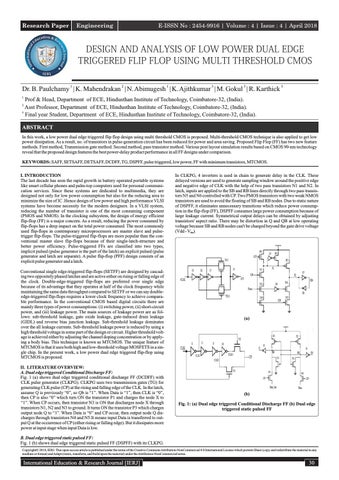
ABSTRACT In this work, a low power dual edge triggered flip flop design using multi threshold CMOS is proposed. Multi-threshold CMOS technique is also applied to get low power dissipation. As a result, no. of transistors in pulse-generation circuit has been reduced for power and area saving. Proposed Flip Flop (FF) has two new feature methods. First method, Transmission gate method. Second method, pass transistor method. Various post layout simulation results based on CMOS 90-nm technology reveal that the proposed design features the best power-delay product performance in all FF designs under comparison. KEYWORDS: SAFF, SETSAFF, DETSAFF, DCDFF, TG, DSPFF, pulse triggered, low power, FF with minimum transistors, MTCMOS. I. INTRODUCTION The last decade has seen the rapid growth in battery operated portable systems like smart cellular phones and palm-top computers used for personal communication services. Since these systems are dedicated to multimedia, they are designed not only for low power consumption but also for the reducing area to minimize the size of IC .Hence design of low power and high performance VLSI systems have become necessity for the modern designers. In a VLSI system, reducing the number of transistor is one of the most consuming component (PMOS and NMOS). In the clocking subsystem, the design of energy efficient flip-flop (FF) is a major concern. As a result, reducing the power consumed by flip-flops has a deep impact on the total power consumed. The most commonly used flip-flops in contemporary microprocessors are master slave and pulsetrigger flip-flops. The pulse-triggered flip-flops are more popular than the conventional master slave flip-flops because of their single-latch-structure and better power efficiency. Pulse-triggered FFs are classified into two types, implicit pulsed (pulse generator is the part of the latch) an explicit pulsed (pulse generator and latch are separate). A pulse flip-flop (PFF) design consists of an explicit pulse generator and a latch. Conventional single edge-triggered flip-flops (SETFF) are designed by cascading two oppositely phased latches and are active either on rising or falling edge of the clock. Double-edge-triggered flip-flops are preferred over single edge because of its advantage that they operates at half of the clock frequency while maintaining the same data throughput compared to SETFF or we can say doubleedge-triggered flip-flops requires a lower clock frequency to achieve comparable performance. In the conventional CMOS based digital circuits there are mainly three types of power consumptions: (i) switching power, (ii) short-circuit power, and (iii) leakage power. The main sources of leakage power are as follows: sub-threshold leakage, gate oxide leakage, gate-induced drain leakage (GIDL) and reverse bias junction leakage. Sub-threshold leakage dominates over the all leakage currents. Sub-threshold leakage power is reduced by using a high threshold voltage in some part of the design or circuit. Higher threshold voltage is achieved either by adjusting the channel doping concentration or by applying a body bias. This technique is known as MTCMOS. The unique feature of MTCMOS is that it uses both high and low-threshold voltage MOSFETS in a single chip. In the present work, a low power dual edge triggered flip-flop using MTCMOS is proposed. II. LITERATURE OVERVIEW: A. Dual edge triggered Conditional Discharge FF: Fig. 1 (a) shows dual edge triggered conditional discharge FF (DCDFF) with CLK pulse generator (CLKPG). CLKPG uses two transmission gates (TG) for generating CLK pulse (CP) at the rising and falling edge of the CLK. In the latch, assume Q is previously “0”, so Qb is “1”. When Data is “1”, then CLK is “0”, then CP is also “0” which turn ON the transistor P1 and charges the node X to “1”. When CP occurs, then transistor N3 is ON that discharges node X through transistors N1, N2 and N3 to ground. It turns ON the transistor P3 which charges output node Q to “1”. When Data is “0” and CP occur, then output node Q discharges through transistors N4 and N5.It means input Data is transferred to output Q at the occurrence of CP (either rising or falling edge). But it dissipates more power at input stage when input Data is low.
In CLKPG, 4 inverters is used in chain to generate delay in the CLK. These delayed versions are used to generate sampling window around the positive edge and negative edge of CLK with the help of two pass transistors N1 and N2. In latch, inputs are applied to the SB and RB lines directly through two pass transistors N5 and N6 controlled with CP. Two PMOS transistors with two weak NMOS transistors are used to avoid the floating of SB and RB nodes. Due to static nature of DSPFF, it eliminates unnecessary transitions which reduce power consumption in the flip-flop (FF), DSPFF consumes large power consumption because of large leakage current. Symmetrical output delays can be obtained by adjusting transistors' aspect ratio. There may be distortion in Q and QB at low operating voltage because SB and RB nodes can't be charged beyond the gate drive voltage (Vdd - Vthn).
(a)
(b) Fig. 1: (a) Dual edge triggered Conditional Discharge FF (b) Dual edge triggered static pulsed FF
B. Dual edge triggered static pulsed FF: Fig. 1 (b) shows dual edge triggered static pulsed FF (DSPFF) with its CLKPG. Copyright© 2018, IERJ. This open-access article is published under the terms of the Creative Commons Attribution-NonCommercial 4.0 International License which permits Share (copy and redistribute the material in any medium or format) and Adapt (remix, transform, and build upon the material) under the Attribution-NonCommercial terms.
International Education & Research Journal [IERJ]
30
Research Paper
E-ISSN No : 2454-9916 | Volume : 4 | Issue : 4 | April 2018 Here, we used Signal feed through FF with three changes; first, we apply CLK pulse at gate of transistor P1 by removing ground from gate terminal; second, we use MTCMOS technique; and third, we remove one inverter from the output of FF for getting Qbar. Number of transistors in Signal feed through FF and proposed FF are same but proposed FF has lower power dissipation and delay with respect to Signal feed through FF. When CLK=0, then no CLK pulse is generated but it charges intermediate node X through transistor P1. Assume output Q is initially “0”, so Qbar is “1”. If the input Data is “1” then node X is discharged with the occurrence of CLK pulse Z. It will start charging node Q through transistor P2. But at the same time, transistor N4 is ON with the CLK pulse, that also charges (or give push) to the node Q because node Q is directly connected to the input Data through transistor N4. And when Data becomes “0”, then node X doesn't discharge, but with the occurrence of CLK pulse, node Q discharges through transistor N4 to the input Data instantly.
III. PROPOSED DETFF DESIGN: Here, we already described some dual edge triggered FF which has more power dissipation ,so that we using transistor reducing method.1.transmission gate method, using CMOS types of transistor reducing large amount of area and power.2.Pass transistor method ,using PMOS &NMOS types of transistor to reduce power consumption.
IV. SIMULATION RESULTS: Pass transistor method(pmos&nmos) and transmission gate method (cmos) are simulated for the better performance. All simulation results are evaluated at 90nm CMOS process technology using DSCH and MICROWIND tool with 1V power supply. CLK frequency used in single edge triggered FFs. FFs are loaded with 20fF capacitance at the output. Conventional FFs are simulated with 0.18V threshold voltage, but proposed FF used 0.18V and 0.36V threshold voltage.This can be archieved with clk1and clk2.Fig.4. Shows the simulation waveform of proposed dual edge triggered FF of transmission gate method.
Fig. 2: Representation of PMOS, NMOS and CMOS transistors Here, we are using EXOR gate based dual edge triggered CLK pulse generator. Main concept behind this approach is described in figure.3
Fig. 4: Simulation waveform of proposed dual edge triggered flipflop of pass transistor method Here, Table shows the power comparision of existing method and proposed FF with signal feed through technique using MTCMOS and this shows leakage power dissipation comparison. It is clearly noticed that proposed FF with MTCMOS has highest performance and low leakage power dissipation. EXISTING FF (a)
PROPOSED FF Gate transmission Pass transistor
No. of Transistors
28
20
24
Min. D-to-Q Delay (ps)
155.12
121.74
85.73
Power (100%) uW
31.09
24.04
14.75
Power (50%) uW Power (25%) uW
25.33 21.33
14.98 08.89
11.39 07.50
V. CONCLUSION: This paper presents the design and analysis of low power dual edge triggered FF using MTCMOS technique with reducing transistor, 1V power supply and 90nm CMOS process technology. MTCMOS uses MOSFET's with two different methods (pass transistor and gate transmission) on a single chip. Gate transmission MOSFET's improving the speed performance at a low supply voltage of 1 V, while pass transistor MOSFET's suppress the standby power dissipation. Obtained results shows low D-to-Q delay, lower power dissipation than previous single edge triggered FF. we can reduce the no. of transistors in NOR gate to speed up the transition and low power simulation. (b) Fig. 3: (a) input of gate transmission method, (b) input of the pass transistor method
31
REFERENCES: 1.
A. P. Chandrakasan, S. Sheng, and R W. Brodersen, “Low-Power CMOS Digital Design,” IEEE Journal of Solid-State Circuits, vol. 27, no. 4, pp. 473-484, April 1992.
2.
H. Kawaguchi and T. Sakurai, “A Reduced Clock-Swing Flip-Flop (RCSFF) for 63% PoweReduction,” IEEE Journal of Solid-State Circuits, vol. 33, no. 5, pp. 807-11, May
International Education & Research Journal [IERJ]
Research Paper
E-ISSN No : 2454-9916 | Volume : 4 | Issue : 4 | April 2018
1998. 3.
A. P. Chandrakasan, W. J. Bowhill, and F. Fox, “High-Performance Microprocessor Circuits,” 1st ed. Piscataway, NJ: IEEE Press,2001.
4.
P. Zhao, J. McNeely, W. Kuang, N. Wang, and Z. Wang, “Design of sequential elements for low power clocking system,” IEEE Transactions on Very Large Scale Integration (VLSI) Systems, vol. 19, no. 5, pp. 914918, May 2011.
5.
J. Tschanz, S. Narendra, Z. Chen, S. Borkar, M. Sachdev, and V. De,
6.
“Comparative Delay and Energy of Single Edge-Triggered & Dual EdgeTriggered Pulsed Flip-Flops for High-Performance Microprocessors,” ISLPED'01, pp. 147-152, Aug. 2001.
7.
V. Stojanovic and V. Oklobdzija, “Comparative analysis of master-slave latches and flip-flops for high-performance and low-power systems,” IEEE J. Solid-State Circuits, vol. 34, no. 4, pp. 536–548, Apr. 1999.
8.
S. Mutoh, T. Douseki, Y. Matsuya, T. Aoki, S. Shigematsu, and J. Yamada, “1 -V Power Supply High-speed Digital Circuit Technology with Multithreshold-Voltage CMOS,” IEEE Journal of Solid-State Circuits, vol. 30, no. 8, pp. 847-54, Aug. 1995.
9.
P. Zhao, T. Darwish, and M. Bayoumi, “High-performance and lowpower conditional discharge flip-flop ,” IEEE Transaction on Very Large Scale Integration (VLSI) Systems, vol. 12, no. 5, pp. 477-484, May 2004.
10. G. Aliakbar and M. Hamid, "Dual-edge triggered static pulsed flip-flops," 18th IEEE International Conference on VLSI Design, pp. 846-849, Jan. 2005. 11. N. K. Saini and K. K. Kashyap, “Low Power Dual Edge Triggered FlipFlop,” IEEE International Conference onSignal Propagation and Computer Technology (ICSPCT), pp. 125-128, July 2014. 12. J.F. Lin, “Low-power pulse-triggered flip-flop design based on a signal feed-through scheme” IEEE Transaction on Very Large Scale Integration (VLSI) Systems, vol. 22, no. 1, pp. 181-185, Jan 2014.
International Education & Research Journal [IERJ]
32