CHAPTER 2
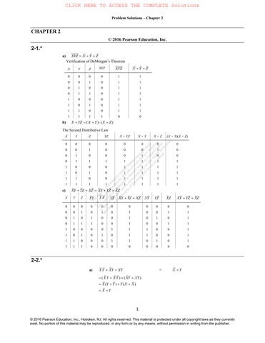
2-1.*
a)
© 2016 Pearson Education, Inc.
Verification of DeMorgan’s Theorem
The Second Distributive Law
ThisworkisprotectedbyUnitedStatescopyrightlaws andisprovidedsolelyfortheuseofinstructorsinteaching theircourses andassessingstudentlearning. Dissemination orsaleofanypartofthiswork(includingontheWorldWideWeb) willdestroytheintegrityoftheworkandisnotpermitted.
2-3.
b)
c)
XYXYZXYZXZXYYZ
XYZXYZXZXYYZ
XYXZYXYYZ
XYXZXYZZYZ
XYXZXYZYZX
XYXZYYZ
XYXZYZ
ThisworkisprotectedbyUnitedStatescopyrightlaws andisprovidedsolelyfortheuseofinstructorsinteaching theircourses andassessing studentlearning. Dissemination orsaleofanypartofthis work(includingontheWorldWideWeb)willdestroytheintegrityoftheworkandisnotpermitted.
ABCABCBCBCDBCDCD
ABCCBCDDBCCD
ABBCBCCD
BABCD
BCD
b) WYWYZWXZWXY = WYWXZXYZXYZ ()( )( )( ) ()( )( )( ) ()()()
c)
WYWXYZWXYZWXYZWXYZWXYZWXYZWXYZ WYWXYZWXYZWXYZWXYZWXYZWXYZWXYZ WYWXZYYXYZWWXYZWW WYWXZXYZXYZ
ADABCDBC = ( )( )ABCDABCD
2-4.+
2-5.+
2-6.
Given: 0,1ABAB
Prove: ()()() ACABBC = BC ( )() 0() ()(0) ()() ( ABACBCBC
ABACBC CAB CAB CABAB CABABB BC
Step 1: Define all elements of the algebra as four bit vectors such as A, B and C:
A = (A3, A2, A1, A0)
B = (B3, B2, B1, B0)
C = (C3, C2, C1, C0)
Step 2: Define OR1, AND1 and NOT1 so that they conform to the definitions of AND, OR and NOT presented in Table 2-1.
a) A + B = C is defined such that for all i, i = 0, ... ,3, Ci equals the OR1 of Ai and Bi
b) A B = C is defined such that for all i, i = 0, ... ,3, Ci equals the AND1 of Ai and Bi.
c) The element 0 is defined such that for A = “0”, for all i, i = 0, ... ,3, Ai equals logical 0.
d) The element 1 is defined such that for A = “1”, for all i, i = 0, ... ,3, Ai equals logical 1.
e) For any element , AA is defined such that for all i, i = 0, ... ,3, iA equals the NOT1 of Ai
a) () ACABCBCACABCABCBC ( () ACABCABCBC ACACBCABC
ThisworkisprotectedbyUnitedStatescopyrightlaws andisprovidedsolelyfortheuseofinstructorsinteaching theircoursesandassessingstudentlearning. Dissemination orsaleofanypartofthiswork(includingontheWorldWideWeb) willdestroytheintegrityoftheworkandis notpermitted.
AABCABBCABCC ABCABCABCABC
c) ()() ABCACABCCABC d) ABDACDBD () ABBACD () AACBD ()ABD
e) ()()() ABACABC AAABCACABCBAABCBCABC ABC
2-7.*
a)
()()()()() XYXYZXYXXYZXXYXZXXXYXZ ()() XYXZXYZ
b) ()()()() XYZXZXYZXZXYZXZZXYZXY ()() XXXYYZXYYZXY
c) ()() WXZYZXWWYZWXZWXYZWXWXYZ WXZWXZWXWXWXX
d) ()() ABABCDCDACABCDABCDABCDABCDAC
()() ABCDACACABCDACCBDACBD
2-8. a)
c) Same as part b.
2-9.*
2-10.*
a) ()() FABAB
b) (()) FVWXYZ
c) [()()][] FWXYZYZWXYZYZ
Truth Tables a, b, c
ThisworkisprotectedbyUnitedStatescopyrightlaws andisprovidedsolelyfortheuseofinstructorsinteaching theircoursesandassessingstudentlearning. Dissemination orsaleofanypartofthiswork(includingontheWorldWideWeb) willdestroytheintegrityoftheworkandisnotpermitted.
a) Sum of Minterms: XYZXYZXYZXYZ
Product of Maxterms: ()()()() XYZXYZXYZXYZ
b) Sum of Minterms: ABCABCABCABC
Product of Maxterms: ()()()() ABCABCABCABC
c) Sum of Minterms: WXYZWXYZWXYZWXYZWXYZWXYZ WXYZ
Product of Maxterms: ()()() WXYZWXYZWXYZ ()()() WXYZWXYZWXYZ ()()() WXYZWXYZWXYZ
2-11.
a) (1, 2, 4, 6)(0, 3, 5, 7), Em M (0, 2, 4, 7)(1, 3, 5, 6) Fm M
b) (0, 3, 5, 7), Em (1, 3, 5, 6) Fm
c) (0,1, 2, 4, 6, 7), EFm (2, 4) EFm
d) ,EXYZXYZXYZXYZ FXYZXYZXYZXYZ
e) (), EZXYXYZ () FZXYXYZ
2-12.*
a) ()() ABCBCDABABCDBCABBC s.o.p. ()BAC p.o.s.
b) ()()()(()()) XXXYYZXXXXYYZ ()() XXYXYZ p.o.s. (1)()YXYZXYZ s.o.p.
c) ()()()()()() ABCCDBEFABCABDACDBEF ()()()()() ABCABDACDBEBF p.o.s. ()()()()() ABCCDBEFABEFBCBEFCDBEF ABAEFBCEFBCDCDEF s.o.p.
ThisworkisprotectedbyUnitedStatescopyrightlaws andisprovidedsolelyfortheuseofinstructorsinteaching theircoursesandassessingstudentlearning. Dissemination orsaleofanypartofthiswork(includingontheWorldWideWeb) willdestroytheintegrityoftheworkandisnotpermitted.
2-14.
2-15.*
2-16.
ThisworkisprotectedbyUnitedStatescopyrightlaws andisprovidedsolelyfortheuseofinstructorsinteaching theircoursesandassessingstudentlearning. Dissemination orsaleofanypartofthiswork(includingontheWorldWideWeb) willdestroytheintegrityoftheworkandisnotpermitted.
2-17.
2-18.*
2-19.*
2-20. a) ,,,, PrimeBDACDABCABCACD b) ,,,,, PrimeWYXYWXZWXXYZWYZ ,,, EssentialACDABCABCACD , EssentialWYXY RedundantBD ,, RedundantWXXYZWYZ
FACDABCABCACD FWYXYWXZ
c) ,,,,,, PrimeWZXZWYZXYZWXYWXZWXY , EssentialWZXZ ,, Redundant=WXYWXZWXY
FWZXZWYZXYZ
2-21.
ThisworkisprotectedbyUnitedStatescopyrightlaws andisprovidedsolelyfortheuseofinstructorsinteaching theircoursesandassessingstudentlearning. Dissemination orsaleofanypartofthiswork(includingontheWorldWideWeb) willdestroytheintegrityoftheworkandisnotpermitted.
(3,4,5,6,7,9,11,13) Fm (0, 2, 6, 7, 8, 9, 10, 12, 14, 15) Fm FWXWYZXYZ FBDBCABCAD ()()() FWXWYZXYZ ()()()()
2-22.*
2-23.
a) s.o.p. ABDABCABDABC b) s.o.p. XYZWZ or ACDBCDACDBCD p.o.s. ()() XYZWXZ
p.o.s. ()()()() ABDABCABDABC or ()()()() ACDBCDACDBCD
2-24. FAC ( ) or ( ) or () FADABDBCD ACDBCDABDABC FXYZWXYWYZXYZ
2-25.*
= Essential XZ = F XZ WXY WXY + + =
2-26.
Primes AB AC BC ABC = F AB AC BC + + = Essential AB AC BC = Primes XZ XZ WXY WXY WYZ WYZ
Primes AB C AD BD = Essential C AD = F C AD BD or AB + + = ,,, PrimesABACBCABC ,,,,, PrimesXZXZWXYWXYWYZWYZ , ,, PrimesABCADBD , , EssentialABACBC EssentialXZ , EssentialCAD FABACBC
ThisworkisprotectedbyUnitedStatescopyrightlaws andisprovidedsolelyfortheuseof instructorsinteachingtheircoursesandassessingstudentlearning. Dissemination orsaleofanypartofthiswork(includingontheWorldWideWeb) willdestroytheintegrityoftheworkandisnotpermitted.
2-27.*
XYXYXY
Dual(X)Dual() YXYXY
()() XYXY
XYXY
XYXY
XY
2-28. ()ABCDADADABCDAD
Note that () XYXYXY
Letting and, XABCDYAD
We can observe from the map below or determine algebraically that XY is equal to 0.
For this situation, () XYXYXY ()0 XY XY
So, we can write (, , , )() FABCDXYABCDAD
The longest path is from input CorD.
2-30.
2-31.
a) b) c)
2-32.
a)t2t2 t2(0.36)2(0.20)1.12 ns
PHL-C, D to FPLHPHL
t2t2t2(0.20)2(0.36)1.12 ns
t1.12 ns
PLH-C, D to FPHLPLH pd
t2tt2(0.20)(0.36)0.76 ns
PHL-BPHLPLH to F
PLH-BPHLPLH to F
t2tt2(0.36)(0.20)0.
92 ns
t0.760.920.84 ns
pd-B to F
ttt0.360.200.56 ns
PHL-A,PLHPHL B, C to F
ttt0.200.360.56 ns
PLH-A,PHLPLH B, C to F
t0.56 ns
pd-A, B, C to F
b)t4t4(0.28)1.12ns
t3t3(0.28)0.78ns
t toF2t2(0.28)0.56ns
pd-C, D to Fpd pd pd-B to F pd-A, B, C pd
c) For paths through an odd number of inverting gates with unequal gate tPHL and tPLH, path tPHL, tPLH, and tpd are different. For paths through an even number of inverting gates, path tPHL, tPLH, and tpd are equal.
ThisworkisprotectedbyUnitedStatescopyrightlaws andisprovidedsolelyfortheuseofinstructorsinteaching theircoursesandassessingstudentlearning. Dissemination orsaleofanypartofthiswork(includingontheWorldWideWeb) willdestroytheintegrityoftheworkandisnotpermitted.
If the rejection time for inertial delays is greater than the propagation delay, then an output change can occur before it can be predicted whether or not it is to occur due to the rejection time. For example, with a delay of 2 ns and a rejection time of 3 ns, for a 2.5 ns pulse, the initial edge will have already appeared at the output before the 3 ns has elapsed at which whether to reject or not is to be determined.
2-33.+
2-34.*
a) The propagation delay is pd PHL PLH max(0.05, 0.10)0.10ns. ttt
a)Thepropagation delayistpd = max( tPHL = 0.05, tPLH = 0.10) = 0.10 ns.
2-35.
Assuming that the gate is an inverter, for a positive output pulse, the following actually occurs:
a)Thepropagation delayistpd = max( tPHL = 0.05, tPLH = 0.10) = 0.10 ns.
Assuming that the gate is an inverter, for a positive output pulse, the following actually occurs:
Assuming that the gate is an inverter, for a positive output pulse, the following actually occurs:
If the input pulse is narrower than 0.05 ns, no output pulse occurs so the rejection time is 0.05 ns. The resulting model predicts the following results, which differ from the actual delay behavior, but models the rejection behavior: :
If the input pulse is narrower than 0.05 ns, no output pulse occurs so the rejection time is 0.05 ns. The resulting model predicts the following results, which differ from the actual delay behavior, but models the rejection behavior: : 0.10 ns 0.05 ns
0.10 ns 0.10 ns
If the input pulse is narrower than 0.05 ns, no output pulse occurs so the rejection time is 0.05 ns. The resulting model predicts the following results, which differ from the actual delay behavior, but models the rejection behavior: : 0.10 ns 0.05 ns 0.10 ns 0.10 ns
b)For a negative output pulse, the following actually occurs: b)For anegativeoutput pulse,thefollowing actuallyoccurs:
The model predicts the following results, which differs from the actual delay behavior and from the actual rejection behavior: b)For anegativeoutput pulse,thefollowing actuallyoccurs: The model predicts the following results, which differs from the actual delay behavior and from theactual rejection behavior:
ThisworkisprotectedbyUnitedStatescopyrightlaws andisprovidedsolelyfortheuseofinstructorsinteaching theircoursesandassessingstudentlearning. Dissemination orsaleofanypartofthiswork(includingontheWorldWideWeb) willdestroytheintegrityoftheworkandisnotpermitted.
0.10 ns
The model predicts the following results, which differs from the actual delay behavior and from theactual rejection behavior:
Overall,themodel isinaccuratefor both casesaand b,and providesafaultyrejection model for case b. Using an average of t PHL and t PLH for t pd would improve the delay accuracyof themodel for circuit applications,but therejection model still fails.
Overall,themodel isinaccuratefor both casesaand b,and providesafaultyrejection model for case b. Using an average of t PHL and t PLH for t pd would improve the delay accuracyof themodel for circuit applications,but therejection model still fails.
Overall, the model is inaccurate for both cases a and b, and provides a faulty rejection model for case b. Using an average of tPHL and tPLH for tpd would improve the delay accuracy of the model for circuit applications, but the rejection model still fails.
Figure 4-40: Structural VHDL Description library ieee; use ieee.std_logic_1164.all; entity nand2 is port(in1, in2: in std_logic; out1 : out std_logic); end nand2;
architecture concurrent of nand2 is begin out1 <= not (in1 and in2); end architecture;
library ieee; use ieee.std_logic_1164.all; entity nand3 is port(in1, in2, in3 : in std_logic; out1 : out std_logic); end nand3;
architecture concurrent of nand3 is begin out1 <= not (in1 and in2 and in3); end concurrent;
library ieee; use ieee.std_logic_1164.all; entity nand4 is port(in1, in2, in3, in4: in std_logic; out1 : out std_logic); end nand4;
The code above this point could be eliminated by using the library, func_prims.
library ieee;
use ieee.std_logic_1164.all; entity fig440 is port(X: in std_logic_vector(2 to 0); f: out std_logic); end fig440; architecture structural_2 of fig440 is
component NAND2
port(in1, in2: in std_logic; out1: out std_logic); end component;
component NAND3
port(in1, in2, in3: in std_logic; out1: out std_logic); end component;
signal T: std_logic_vector(0 to 4); begin
ThisworkisprotectedbyUnitedStatescopyrightlaws
andisprovidedsolelyfortheuseofinstructorsinteaching theircoursesandassessingstudentlearning. Dissemination orsaleofanypartofthiswork(includingontheWorldWideWeb) willdestroytheintegrityoftheworkandisnotpermitted.
g0: NAND2 port map (X(2),X(1),T(0));
g1: NAND2 port map (X(2),T(0),T(1));
g2: NAND2 port map (X(1),T(0),T(2));
g3: NAND3 port map (X(1),T(1),T(2),T(3));
g4: NAND2 port map (X(1),T(2),T(4));
g5: NAND2 port map (T(3),T(4),f); end structural_2;
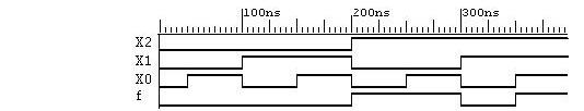
0210 FXXXX F =X0X2 + X1X2
2-36.
g0: NOT_1 port map (D, x1);
begin
g1: AND_2 port map (B, C, x2);
g0: NOT_1 port map (D, x1); XDBC
g2: NOR_2 port map (A, x1, x3);
g1: AND_2 port map (B, C, x2); YABCD
g3: NAND_2 port map (x1, x3, x4);
g2: NOR_2 port map (A, x1, x3);
g4: OR_2 port map (x1, x2, x5);
g3: NAND_2 port map (x1, x3, x4);
g5: AND_2 port map (x4, x5, X);
g4: OR_2 port map (x1, x2, x5);
g6: AND_2 port map (x3, x5, Y); end structural_1;
g5: AND_2 port map (x4, x5, X);
g6: AND_2 port map (x3, x5, Y); end structural_1;

2-37.
2-38.* begin F <= (X and Z) or ((not Y) and Z); end;
2-39.*
ThisworkisprotectedbyUnitedStatescopyrightlaws andisprovidedsolelyfortheuseofinstructorsinteaching theircoursesandassessingstudentlearning. Dissemination orsaleofanypartofthiswork(includingontheWorldWideWeb) willdestroytheintegrityoftheworkandisnotpermitted.
2-40.
module circuit_4_50(A, B, C, D, X, Y); input A, B, C, D; output X, Y; wire n1, n2, n3, n4, n5; not go(n1, D); nand g1(n4, n1, n3); and g2(n2, B, C), g3(X, n4, n5), g4(Y, n3, n5); or g5(n5, n1, n2); nor g6(n3, n1, A); endmodule
ThisworkisprotectedbyUnitedStatescopyrightlaws andisprovidedsolelyfortheuseofinstructorsinteaching theircoursesandassessingstudentlearning. Dissemination orsaleofanypartofthiswork(includingontheWorldWideWeb) willdestroytheintegrityoftheworkandisnotpermitted.
2-41.
module circuit_4_51(X, F); input [2:0] X; output F; wire [0:4] T; nand
module circuit_4_51(X, F); input [2:0] X; output F; wire [0:4] T; nand
g0(T[0],X[0],X[1]), g1(T[1],X[0],T[0]), g2(T[2],X[1],T[0]), g3(T[3],X[2],T[1],T[2]), g4(T[4],X[2],T[2]), g5(F,T[3],T[4]); endmodule
g0(T[0],X[0],X[1]), g1(T[1],X[0],T[0]), g2(T[2],X[1],T[0]), g3(T[3],X[2],T[1],T[2]), g4(T[4],X[2],T[2]), g5(F,T[3],T[4]); endmodule
2-42.
2-43.*
ThisworkisprotectedbyUnitedStatescopyrightlaws
module circuit_4_53(X, Y, Z, F); input X, Y, Z; output F; assign F = (X & Z) | (Z & ~Y); endmodule
andisprovidedsolelyfortheuseofinstructorsinteaching theircoursesandassessingstudentlearning. Dissemination orsaleofanypartofthiswork(includingontheWorldWideWeb) willdestroytheintegrityoftheworkandisnotpermitted.