1. INTRODUCTION
Article Info ABSTRACT
Nur Syafiqah Nadiah Mohd Alias1, Faiz Arith1 , Nur Syamimi Noorasid1, Hafez Sarkawi2 , Ahmad Nizamuddin Muhammad Mustafa2, Mohd Muzafar Ismail2 , Mohd Khanapiah Nor2 1Faculty of Electronic and Computer Engineering, Universiti Teknikal Malaysia Melaka, Hang Tuah Jaya 76100 Melaka, Malaysia 2Faculty of Electrical and Electronic Engineering Technology, Universiti Teknikal Malaysia Melaka, Hang Tuah Jaya 76100 Melaka, Malaysia
Corresponding Author: Faiz FacultyArithof
NiDSSCdoped ZnO Scaps 1D
Email: faiz.arith@utem.edu.my
TELKOMNIKA Telecommunication Computing Electronics and Control Vol. 20, No. 5, October 2022, pp. 1117~1124
This is an open access article under the CC BY SA license.
1117
In recent years, dye sensitized solar cells (DSSC) have gained attention with good photovoltaic performance, specifically under low light conditions along with flexibility in terms of color and structure In addition, DSSC is also known for its simple fabrication procedures and low production costs. The first DSSC was reported by Regan and Grätzel in 1990s, using mesoporous titanium oxide (TiO2) prepared from colloidal TiO2 nanoparticles for light absorption [1]. DSSC is photo electrochemical cell based, in which energy generation for charge carrier transport is driven from the absorption of photon energy and produces a chemical reaction [2]. However, there are many challenges faced by DSSC to improve power conversion efficiency (PCE) without reducing the stability characteristics. Theoretically, the external circuit through the semiconductor photo anode needs to function properly so that the absorption of light by the organic dye can generate and produce a flow of current which in turn produces energy, and this is known as the electrochemical effect. The semiconductor photo electrode layer plays an important role when current reduction occurs during the recombination of photo generated carriers in the semiconductor which in turn reduces the efficiency of the solar cell. On the other hand, the photo anode must be highly transparent to allow sunlight to reach the dye molecules. The concept working mechanism of DSSC was different compared to other types of the solar cell, where DSSC is a photoelectrochemical solar cell that contains a dye sensitized
Journal homepage: http://telkomnika.uad.ac.id
Article history:
Accepted Jul 27, 2022
Electronic and Computer Engineering, Universiti Teknikal Malaysia Melaka Hang Tuah Jaya, 76100 Durian Tunggal, Melaka, Malaysia
Received Jan 17, 2022
Study the effect of nickel and aluminium doped ZnO photoanode in DSSC
Dye sensitized solar cells (DSSC) is one of the promising candidates which are efficient, low cost, and clean hybrid molecular solar cell devices. Zinc oxide (ZnO) has been widely used as the phoanode in DSSC due to its excellent charge conduction mechanism, yet still suffers from poor cell efficiency. In this study, aluminium doped ZnO (ZnO:Al) and Ni doped ZnO (ZnO:Ni) were studied as photoanode material in DSSC using solar cell capacitance simulator (SCAPS) simulation, and the electrolyte liquid considered a single solid p type layer as hole transporting materials. Both studied photoanodes have demonstrated better cell performance than pure ZnO photoanode due to the small amount of aluminium (Al) and nikel (Ni) impurities added have enhanced the physiochemical properties of ZnO films. A power conversion efficiency (PCE) of 3.96% was obtained at 3 mol% ZnO:Al photoanode with optimized key parameters. These simulation results proved an opportunity to improve the performance of the DSSCs via doping engineering into the ZnO photonaode.
Al doped ZnO Buffer layers
Revised Jul 17, 2022
ISSN: 1693 6930, DOI: 10.12928/TELKOMNIKA.v20i5 23013
Keywords:

In this works, the performance of DSSC with Al and Ni doped ZnO as photoanode were investigated using solar cell capacitance simulator (SCAPS) simulation software. Several key parameters including layer thickness, doping concentration, operating temperature as well as defect density were studied in order to obtain a optimum value of PCE in DSSC structureIt is observed that the electrical conductivity in ZnO photoanode is able to increase hgiher with dopant a small amount of material Al and Ni. The best cell performance was achieved with 3 mol% and 4 mol% Al doped ZnO photoanode, which produced PCE of 3.96%. Similarly, Ni doped ZnO photoanode of concentration 4 mol% and 6 mol% provided PCE as high as 3.9% compared to PCE without doped ZnO photoanode which is low. The PCE in DSSC is able to increase and provide best cell performance as the concentration of material increase, however at certain point, Al3+ and Ni2+ consist of a solubility limit to substitute in ZnO material and these findings were found in previous reports [9] [12]. The obtained results can be used as a guide and direction for future device fabrication.
2. DSSC SIMULATION
1118mesoporous
ISSN: 1693 6930 Telecommun Comput El Control, Vol. 20, No. 5, October 2022: 1117 1124
�� ���� ( ��(��)���� ����)=��[��(��) ��(��)+���� +(��) ���� (��)+����(��) ����(��)] (1) ������ ���� =���� ���� ����0 ���� �������� ���� ���� ������ ������ ���� ���� ��2���� ����2 (2) ������ ���� =���� ���� ����0 ���� �������� ���� ���� ������ ������ ���� ���� ��2���� ����2 (3) Figure
TiO2 work electrode (WE), a redox mediator (electrolyte) and a counter electrode (CE) [1], [3] [5]. However, WE and CE can be (semi) transparent that allowing for illumination of the solar cell. Since the beginning of TiO2 based DSSC research, zinc oxide (ZnO) has been the best TiO2 alternative for DSSC. Both TiO2 and ZnO consists same electron affinities and almost same band gap energies approximately 3.2 eV and 3.3 eV, respectively, and ZnO has much higher electron diffusivity than TiO2 [6], [7] and higher electron mobility of 115 cm2 V 1 s 1 155 cm2 V 1 s 1 [8], which is for efficient electron transport in the semiconductor and reduction of recombination rate. The electrical conductivity of ZnO can be enhanced further with a small amount of aluminium (Al) and nikel (Ni) impurities. The ion radius of Zn2+ (0.74 Å) are larger than Al3+ (0.54 Å) and Ni2+ (0.69 Å), therefore Zn2+ able to replace at the lattice site when a small quantity of Al3+ and Ni2+ enters. Subsequently, an additional dopant can be used to improve the conductivity of the ZnO photoanode while maintaining excellent transparency in the visible light region [9], [10].
SCAPS, a one dimensional computer simulation software was used in this work where it was able to simulate the characteristics of solar cells in terms of AC and DC electricity. This simulation software is based on three coupled differential equations that is Poisson’s (1) and continuity equations for holes (2) and electrons (3) where �� is diffusion coefficient, �� is electrostatic potential, �� is electron charge, �� is generation rate, �� is permittivity, and ��, ��, ���� and ���� are free holes, electrons, trapped holes, and trapped electrons, repectively. Meanwhile, ionized acceptor like doping concentration is denoted by ���� , and ionized donor like doping concentration is denoted by ���� [13]. 1. The structure of DSSC with aluminium doped ZnO (ZnO:Al) or nickel doped ZnO (ZnO:Ni) photoanodes
TELKOMNIKA
Table 1. Parameters for DSSC layer [14]ITO N719[15]Dye ZnO[9] Concentration of Al (mol%) [9] Concentration of Ni (mol%) [10] Redox[16]1 2 3 4 1 2 4 6 60 500 220 220 220 220 220 180 180 180 180 100 Eg (eV) 3.6 2.37 3.28 3.25 3.1 3.08 3.05 3.18 3.16 3.14 3.13 1.9 (eV) 3.9 4.4 4.4 4.4 4.4 4.4 4.4 4.4 4.4 4.4 3.79 9 9 9 9 9 9 9
10 Nc (1/cm3) 2.2×10 18 2.4×10 20 103×18 103×18 103×18 103×18 103×18 103×18 103×18 103×18 103×18 6.0×10 21 Nv (1/cm3) 1.8×10 19 2.5×10 20 1.7×10 19 1.7×10 19 1.7×10 19 1.7×10 19 1.7×10 19 1.7×10 19 1.7×10 19 1.7×10 19 1.7×10 19 6.0×10 21 μe (cm2/Vs) 50 5 43.00 14.03 13.84 13.35 15.02 36.73 37.01 35.49 55.39 0.1 μh (cm2/Vs) 75 5 31 31 31 31 31 31 31 31 31 0.3 ND (1/cm3) 101×19 0 2.9×10 15 7.2×10 18 1.02×10 19 1.46×10 19 1.06×10 19 6.09×10 18 7.53×10 18 8.14×10 18 8.80×10 18 101×15 NA (1/cm3) 0 101×17 0 0 0 0 0 0 0 0 0 101×15 Ve (cm/s) 101×7 101×7 101×7 101×7 101×7 101×7 101×7 101×7 101×7 101×7 101×7 101×7 Vh (cm/s) 101×7 101×7 101×7 101×7 101×7 101×7 101×7 101×7 101×7 101×7 101×7 101×7
Study the effect of nickel and aluminium doped ZnO photoanode in … (Nur Syafiqah Nadiah Mohd Alias)
Figure 2. Energy level diagram of simulated DSSC
In the structure of a solar cell, the thickness of the layer plays a very important role in improving cell performance. Here, the layer thicknesses for Al doped ZnO (ZnO:Al) and Ni doped ZnO (ZnO:Ni) photoanodes were varied with different dopant concentrations in the range of 5 nm to 1000 nm for SCAPS simulations PCE for both ZnO:Al and ZnO:Ni photoanodes showed a gradual increase with layer thickness as shown in Figure 3. However, this trend was different for ZnO photoanodes with no dopant addition, where PCE had declined sharply by 20% at 100 nm thickness compared to 5 nm thickness. This trend persists with no significant change with further increase in layer thickness It was also found that, concentrations of 3 mol% 6 mol% Al and Ni doped ZnO photoanodes have shown higher PCE values for all layer thicknesses compared to others by achieving PCE values as high as 3.9%. The increase in cell efficiency at higher Al and Ni doped ZnO photoanode layer thicknesses can be attributed to enhanced photon absorption,

1119
Telecommun
4.1
X
3.1. Effects of Al and Ni doped ZnO photoanode in thickness
(nm)Thickness
3. RESULTS AND DISCUSSION
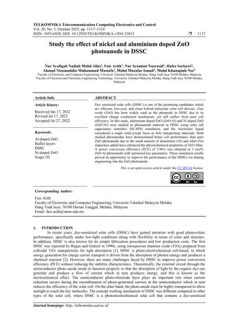
The studied device consists of five main layers which are indium tin oxide (ITO), ZnO:Al or ZnO:Ni as photoanode, N719 dye as dye sensitizer, redox as electrolyte and platinum (Pt) as back contact as shown in Figure 1. The energy level of each layer is illustrated in Figure 2. Herein, the redox acting as an electrolyte is considered to be the solid state �� layer [13]. All parameters for each simulated layer are shown in Table 1. The simulation was performed under an illumination of 1000 W/m2 and an air mass of 1.5 G. The main objective of this work is to investigate the effect of Al and Ni dopant on the ZnO photoanode and to optimize the key parameters of the layer, thus increase the cell efficiency value. The optimization of the main parameters of ZnO: Al and ZnO: Ni photoanodes in terms of thickness, doping concentration, operating temperature and interface defect density has been extensively studied This work thereby provides a clear insight that with the small addition of Al and Ni dopant on the ZnO photoanode with the optimization of several important parameters has improved the efficiency of DSSC [9], [10].
Ɛ/Ɛo 10 30 9 9
TELKOMNIKA Comput El Control
Where n is the electron concentration, ���� is the electron mobility and �� is the electric charge. The equation in low doping were obtain as: ≈���������� (5)
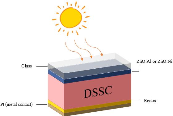
Where �� ≈���� and ���� is the ionized donor concetration. The positive correlation between �� and ���� occurs since the mobility does not change substantially with ���� in case of low doping. It can also be observed that PCE grows slowly as the doping density exceeds 1015 cm 3 . The Moss Burstein effect will create substantial doping effects if doping density continues to rise to a certain point which will limit the DSSC performance [21].
��
more electron hole pairs and thus increasing charge carrier conduction. However, the trend is the differ for pure ZnO without doping, where there is a decrease in PCE with increasing layer thickness. This is probably due to the development of surface containing valleys and peaks at higher thickness [17], [18]. In addition, the chance for recombination to occur is high which results in a decrease in PCE and this is due to the charge requiring a longer journey to conduct current and thus generate energy [19].
��
Figure 3. PCE for Al and Ni doped ZnO photoanodes with different dopant concentrations at different layer thicknesses

Figure 4. Effect of the doping concentrations on the PCE for (a) Al doped ZnO photoanodes DSSC and (b) Ni doped ZnO photoanode DSSC

ISSN: 1693 6930
(a) (b)
3.2. Effects in doping density (ND)
The doping density of ZnO:Al and ZnO:Ni photoanode were varied from 1×1012 cm 3 to 1×1020 cm 3 Figure 4(a) and Figure 4(b) show similar trend curve where the PCE of ZnO:Al and ZnO:Ni photoanode rises gradually as the doping density increases. The increase in photoanode doping concentration will enhance the conductivity and reduce the reverse saturation current, thus leading to PCE growth [20]. Generally, the conductivity (��) in N type doping is establish as: =�������� (4)
1120producing
TELKOMNIKA Telecommun Comput El Control, Vol. 20, No. 5, October 2022: 1117 1124
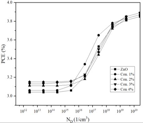
In thin film solar cell applications, the operating temperature has a considerable impact on device performance. The solar cell panels are expected to be functional at temperatures above 300 K. So, in this investigation, operating temperature for both Al and Ni doped ZnO are analyzed from ranged 300 K to 400 K to understand its effect on the cell performance. It can be observed that all PCE devices performance slightly decrease as the temperature rises, approximately by 0.02 ± 0.01 %/K hence proving that an increase in temperature causes an impact on all parameter as shown in Figure 5. As the temperature rises, all parameter includes the material carrier concentration, band gaps, electron and hole mobility values changed, resulting in a reduced cell efficiency [22]. In addition, the significant absorption of energy by electrons at high temperatures causes the efficiency of solar cells to decline with temperature. The electrons are stimulated to move to an unstable state and trigger recombination before entering the conduction band [19], [23].
ZnO ZnO 3.7
TELKOMNIKA Telecommun Comput El
Al doped ZnO 1 3.85
The parameters of the interface layer have a great influence on the perfomance of solar cells. The interface layer quality depends on defect density, where higher defect density generating the recombination rate, thus decreasing the quality of the interface layer. To observe the effect in interface layer of N719 Dye/ZnO:Al and N719 Dye/ZnO:Ni, defect density was varied from range 1×1010 cm 2 to 1×1020 cm 2
Al doped ZnO 4 3.96
Al doped ZnO 2 3.91
3.4. Effects in defect density
Ni doped ZnO 2 3.89
Photoanode Dopant concentration (mol%) CE (%)
3.3. Effects of Al doped ZnO and Ni doped ZnO at different working temperature
Figure 5. Effect of increasing temperature to the ZnO, ZnO:Al and ZnO:Ni photoanodes DSSC
Study the effect of nickel and aluminium doped ZnO photoanode in … (Nur Syafiqah Nadiah Mohd Alias)
At lower value of defect density, ZnO photoanode without doped obtained the lowest PCE which is around 3.06% compared to photoanode with Al doped ZnO and Ni doped ZnO. Furthermore, PCE for N719 Dye/ZnO:Al and N719 Dye/ZnO:Ni interface layer began to show a downward trend at value of 1×1012 cm 2 which can be seen in Figure 6. PCE defect density decreased due to a lower charge recombination rate and carrier recombination at the N719 Dye/ZnO interface, which was achieved by a lower concentration of surface defects in ZnO material [24]. Furthermore, if the interface layer defect density continues to increase, the DSSC performance will degrade because high defect densities in N719 Dye/ZnO:Al and N719 Dye/ZnO: Ni lead to increase the traps and form the recombination centres [25].
1121
Ni doped ZnO 1 3.86
PCE for Al and Ni dopant concetration in ZnO photoanode
Al doped ZnO 3 3.96
Control
Ni doped ZnO 4 3.9
Tableconductivity.2.Optimum
Ni doped ZnO 6 3.9
The optimum PCE values for each Al doped ZnO and Ni doped ZnO photoanode in DSSC that obtained from layer thickness, doping density, operating temperature and defect density are shown in Table 2. It is observed that 3 mol% 6 mol% concentration of Al and Ni yield highest PCE through out the studies. This demonstrate that by adding a small amount of Al and Ni material can increase the performance of ZnO in their electrical
ISSN: 1693 6930 Comput
This work was supported by Universiti Teknikal Malaysia, Melaka, and Ministry of Education Malaysia under grant FRGS/1/2020/FTKEE CETRI/F00454.
[7] N. S. Noorasid, F. Arith, A. N. Mustafa, M. A. Azam, S. H. M Suhaimy, and O.A. Al Ani, “Effect of Low Temperature Annealing on Anatase TiO2 Layer as Photoanode for Dye Sensitized Solar Cell,” Przegląd Elektrotechniczny, vol. 97, pp. 12 16, 2021. [Online]. Available: http://w.pe.org.pl/articles/2021/10/3.pdf
4. CONCLUSION
[8] E. M. Kaidashev et al , “High electron mobility of epitaxial ZnO thin films on cc plane sapphire grown by multistep pulsed laser deposition,” Applied Physics Letters, vol. 82, no. 22, p. 3901, 2003, doi: 10.1063/1.1578694.
REFERENCES
TELKOMNIKA Telecommun
[9] M. M Rahman et al., “Effect of Al Doping on Structural, Electrical, Optical and Photoluminescene Properties of Nano Structural ZnO Thin Films,” Journal of Material Science Technology, vol. 28 No. 4, pp.329 335, 2012, doi: 10.1016/S1005 0302(12)60064 4
[1] B. O’Regan and M. Grätzel, “A low cost, high efficiency solar cell based on dye sensitized colloidal titanium dioxide films,” Nature, vol. 353, pp. 737 740, 1991, doi: 10.1038/353737a0.
[2] K. Sharma, V. Sharma, and S. S. Sharma, “Dye Sensitized Solar Cells: Fundamentals and Current Status,” Nanoscale Research Letters, vo. 13, no. 381, 2018, doi: 10.1186/s11671 018 2760 6
[5] D. Bera, L. Qian, T. K. Tseng, and P. H. Holloway, “Quantum dots and their multimodal applications: a review,” Materials, vol. 3, no. 4, pp. 2260 2345, doi: 10.3390/ma3042260.
[3] X. Chen and S. S. Mao, “Titanium dioxide nanomaterials: synthesis, properties, modifications, and applications,” Chemical reviews, vol. 107, no. 7, pp. 2891 2959, 2007, doi: 10.1021/cr0500535.
6. Cell performance with increasing interface defect density for different dopant of Al doped ZnO, Ni doped ZnO and ZnO photoanode DSSC

[6] R. Vittal and K C Ho, “Zinc oxide based dye sensitized solar cells: A review,” Renewable and Sustainable Energy Reviews, vol. 70, pp. 920 935, 2017, doi: 10.1016/j.rser.2016.11.273.
El Control, Vol. 20, No. 5, October 2022: 1117 1124 1122Figure
ACKNOWLEDGEMENTS
[10] M. Y Ali, M. K. R. Khan, A. M. M. T Karim, M. M Rahman, and M. Kamruzzaman, “Effect of Ni doping on structure, morphology and opto transport properties of spray pyrolised ZnO nano fiber,” Heliyon, vol. 6, no. 3, 2020, doi: 10.1016/j.heliyon.2020.e03588.
Herein, we report the effect of Al and Ni impurities in ZnO photoanode of DSSC on cell performance using SCAPS 1D. DSSC has been succesfully simulated with different doping concentrations along with optimization of several key layer parameters. Cell efficiencies as high as 3.96% and 3.9% were obtained using above 3 mol% ZnO:Al photoanode and 4 mol% ZnO:Ni photoanode, respectively. The cell performance obtained was enhanced than that found in pure ZnO photonoade DSSC, indicating that the additional dopant had improved the charge carrier conduction and thus increased the PCE. However, further increase in dopant concentration above 6 mol% will result in deterioration of cell performance due to larger particle size and Burstein Moss effect. So, this work thereby provides a clear insight that the addition of dopants into ZnO photoanodes with optimized key parameters has successfully improved the performance of DSSC cells. The addition of Ni and Al dopants has contributed to an increase in cell efficiency and in turn further elevates PCE. This is most probably due to the radius of Al3+ and Ni2+ of 0.54 Å and 0.69 Å, respectively, are smaller than the Zn2+, 0.74 Å. Therefore, the Al3+ and Ni2+ ions can sneak in and replace the Zn2+ ions at the lattice site as well as passivate any possible defect in the ZnO photoanode. The results obtained are useful as a guide and direction in the manufacture of future devices.
[4] N. S. Noorasid, et al., “Current advancement of flexible dye sensitized solar cell: A review,” Optik, vol. 254, no 381, 2022, doi: 10.1016/j.ijleo.2021.168089.
Faiz Arith received the B. Eng. in Electrical & Electronic Engineering from University of Fukui, Japan, in 2010. Then he obtained M. Sc in Microelectronic from National University of Malaysia in 2012 and the Ph.D. degree in Semiconductor Devices from Newcastle University, United Kingdom, in 2018. Currently, he is Senior Lecturer and the Head of Micro and Nano Electronic Research Group in Universiti Teknikal Malaysia, Melaka, Malaysia. He is the author of two book chapters, more than 30 articles, and has won several innovation competitions. His main research interest is fabrication and simulation of semiconductor devices including solar cells, MOSFETs, power semiconductor devices and optoelectonic devices. He is a Technical Editor of the Journal of Telecommunication, Electronic and Computer Engineering, and has served as reviewer in more than 10 indexed reputable journals. He can be contacted at email: faiz.arith@utem.edu.my

[17] T. A. N Peiris, H. Alessa, J. S. Sagu, I. A. Bhatti, P. Isherwood, and K. G. U Wijayantha, “Effect of ZnO seed layer thickness on hierarchical ZnO nanorod growth on flexible substrates for application in dye sensitised solar cells,” Journal of Nanoparticle Research, vol. 15, 2013, doi: 10.1007/s11051 013 2115 2.
[16] M. Mehrabian and S. Dalir, “Numerical Simulation of Higly Efficient Dye Sensitized Solar Cell by Replacing the Liquid Electrolyte with a Semiconductor Solid Layer,” Optik, vol. 169, pp. 214 223, 2018, doi: 10.1016/j.ijleo.2018.05.059.
[22] B. M Soucase, I. G. Pradas, and K. R. Adhikari, “Numerical Simulations on Perovskite Photovoltaic Devices,” in Perovskite Materials: Synthesis, Characterisation, Properties, and Applications, LDN, UK: InTechOpen, 2016, Ch. 15 16, doi: 10.5772/61751.


[23] O. V Aliyaselvam, F. Arith, A. N. Mustafa, M. K. Nor, and O. A. Al Ani, “Solution processed of solid state HTL of CuSCN layer at low annealing temperature for emerging solar cell,” International Journal of Renewable Energy Research, vol. 11, no. 2, 2021 [Online]. Available: https://www.researchgate.net/profile/Faiz ofCuSCN_as_a_Hole_Transporting_Layer_for_Perovskite_Solar_Cells_Application/links/610565871e95fe241a9e4b7d/InvestigationArith/publication/347877587_Investigation_of_CopperIThiocyanate_CopperIThiocyanateCuSCNasaHoleTransportingLayerforPerovskiteSolarCellsApplication.pdf
[20] L. Lin, L. Jiang, P. Li, B. Fan, and Y. Qiu, “A modeled perovskite solar cell structure with a Cu2O hole transporting Layer enabling over 20% efficiency by low cost low temperature processing,” Journal of Physics and Chemistry of Solids, vol. 124, pp. 205 211, 2019, doi: 10.1016/j.jpcs.2018.09.024.
[21] K. R Adhikari, S. Gurung, B. K. Bhattarai, and B. M. Soucase, “Comparative study on MAPbI3 based solar cells using different electron transporting materials,” Physica Status Solidi (c), vol. 13, no. 1, pp. 13 17, 2016 doi: 10.1002/pssc.201510078.
[12] N. S. N. M. Alias, F. Arith, A. N. M. Mustafa, M. M. Ismail, S. A. M. Chachuli, and A. S. M. Shah, “Compatibility of Al doped ZnO electron transport layer with various HTLs and absorbers in perovskite solar cells,” Applied Optics, vol. 61, no. 15, pp. 4535 4542, 2022, doi: 10.1364/AO.455550
[11] H. Singh and V. Kumar, “Effect of Ni doping on the photovoltaic conversion efficiency of ZnO nanostructured dye sensitized solar cells,” International Journal of Scientific Research in Physics and Applied Science, vol. 6, no. 3, pp. 50 54, 2018, doi: 10.26438/ijsrpas/v6i3.5054.
[14] A. Chihi, M. F. Boujimil, and B. Bessais, “Investigation on the Performance of CIGS/TiO2 Heterojunction using SCAPS Software for Highly Efficient Solar Cells,” Journal of Electronic Materials, vol. 46, pp. 5270 5277, 2017, doi: 10.1007/s11664 017 5547 0.
[13] M. Burgelman, J. Verschraegen, B. Minnaert, and J. Marlein, “Numerical simulation of thin film solar cells: practical exercises with SCAPS,” in Proceedings of NUMOS (Int. Workshop on Numerical Modelling of Thin Film Solar Cells, 2007, pp. 357 366, doi: 1854/11121.
[19] N. S. Noorasid, F. Arith, A. Y. Firhat, A. N. Mustafa, and A. S. M. Shah, “SCAPS Numerical Analysis of Solid State Dye Sensitized Solar Cell Utilizing Copper (I) Iodide as Hole Transport Layer,” Engineering Journal, vol. 26, no. 2, pp. 1 10, 2022 [Online]. Available: https://www.engj.org/index.php/ej/article/view/4414
Nur Syafiqah Nadiah Mohd Alias received the Dip. in Electronic Engineering and B. Eng in Electronic Engineering from University Teknikal Malaysia Melaka in 2017 and 2020, respectively. Currently, she pursue her study in MSc focusing in Electron Transport Layer for the third generation of solar cell. She can be contacted at email: m022010016@student.utem.edu.my
[15] F. Jahantigh and M. J. Safikhani, “The Effect of HTM on the performance of solid state dye sanitized solar cells (SDSSCs): a SCAPS 1D simulation study,” Applied Physics A., vol. 125, no. 276, 2019, doi: 10.1007/s00339 019 2582 0.
[24] Y Y Lou, S Yuan, Y Zhao, Z Y Wang, and L Y Shi, “Influence of defect density on the ZnO nanostructures of dye sensitized solar cells,” Advances in Manufacturing, vol. 1, pp. 340 345, 2013, doi: 10.1007/s40436 013 0046 x.
[18] R. Pietruszka et al., “New efficient solar cell structures based on zinc oxide nanorods,” Solar Energy Materials and Solar Cells, vol. 143, pp. 99 104, 2015, doi: 10.1016/j.solmat.2015.06.042.
[25] K. Tan, P. Lin, G. Wang, Y. Liu, Z. Xu, and Y. Lin, “Controllable design of solid state perovskite solar cells by SCAPS device simulation,” Solid State Electronics, vol. 126, pp. 75 80, 2016, doi: 10.1016/j.sse.2016.09.012.
BIOGRAPHIES OF AUTHORS
TELKOMNIKA Telecommun Comput El Control
Study the effect of nickel and aluminium doped ZnO photoanode in … (Nur Syafiqah Nadiah Mohd Alias)
1123

Mohd Muzafar Ismail earned his Ph.D. in Atmospheric Discharges from Uppsala University in Sweden under the supervision of Prof. Vernon Cooray. His present research interests focus on atmospheric discharges, specifically lightning electromagnetics, and lightning safety. He is a Graduate Member and Professional Engineer with the Board of Engineers of Malaysia. Presently, he is active in teaching, consulting, and research in the field of lightning and electromagnetics. He can be contacted at email: muzafar@utem.edu.my.
Ahmad Nizamuddin Muhammad Mustafa received the B. Eng. in Electrical & Electronic Engineering from University of Fukui, Japan, in 2009. Then he obtained M. Eng. in Electrical & Electronic Engineering from University of Fukui, Japan, in 2011. Currently, he is a Lecturer at Universiti Teknikal Malaysia, Melaka, Malaysia. He has joined Micro and Nano Electronic Research Group of UTeM and has been awarded several research grants related to the semiconductor device research. He has authored or co authored numerous number of publications. His research interests include fabrication and simulation of semiconductor devices such as MOSFET, solar cells, graphene FET and GaAs optoelectonic devices. He can be contacted at email: nizamuddin@utem.edu.my.
Nur Syamimi Noorasid received the Dip. in Electronic Engineering and B. Eng in Electronic Engineering from University Teknikal Malaysia Melaka in 2017 and 2020, respectively. Currently, she pursue her study in MSc focusing in Electron Transport Layer for the third generation of solar cell. She can be contacted at email: m022010022@student.utem.edu.my.

ISSN: 1693 6930
TELKOMNIKA Telecommun Comput El Control, Vol. 20, No. 5, October 2022: 1117 1124 1124
Mohd Khanapiah Nor received his Diploma in Electrical & Information Engineering from Gifu National Institute of Tehchnology, Japan in 2008. He completed his B. Eng in Electrical and Electronic Engineering from Muroran Institute of Technology, Japan in 2010. Then, he received his M. Eng from Universiti of Malaya in 2013. Currently he is a lecturer in Universiti Teknikal Malaysia Melaka (UTeM), Malaysia. He is a certified energy manager and is involved in energy management at UTeM. He is now pursuing his PhD in Engineering majoring in transparent conducting oxide for thin film solar cells application in Universiti Tenaga Nasional (UNITEN), Malaysia. He can be contacted at email: khanapiah@utem.edu.my.


Hafez Sarkawi received his B. Eng. Electrical (Electronics) from Universiti Teknologi Malaysia, Malaysia in 2007. Then, he obtained M. Eng. (Industrial Electronics and Control) from Universiti Malaya, Malaysia in 2012 and Ph.D. degree in Control System Theory from Kyoto University, Japan in 2021. Currently, he is a Lecturer at Universiti Teknikal Malaysia Melaka, Malaysia and researcher in Advanced Sensors & Embedded Controls System group. He has authored and co authored numerous publications and was awarded several research grants. His research interests include power electronics and control. He can be contacted at email: hafez@utem.edu.my.
