TELKOMNIKA Telecommunication Computing Electronics and Control
Vol. 21, No. 4, August 2023, pp. 872~880
ISSN: 1693-6930, DOI: 10.12928/TELKOMNIKA.v21i4.22341
872
TELKOMNIKA Telecommunication Computing Electronics and Control
Vol. 21, No. 4, August 2023, pp. 872~880
ISSN: 1693-6930, DOI: 10.12928/TELKOMNIKA.v21i4.22341
872
Ramchandra Gurjar, Deepak Kumar Mishra
Department of Electronics and Instrumentation Engineering, Shri G S Institute of Technology and Science, Indore, India
Article Info
Article history:
Received Nov 30, 2021
Revised Aug 08, 2022
Accepted Oct 26, 2022
Keywords:

Figure of merit
Low phase noise
MOS varactor
Tuning range
Voltage controlled oscillator
ABSTRACT
Voltage controlled oscillator (VCO) offers the radio frequency (RF) system designer a freedom to select the required frequency. Today’s wireless communication system imposes a very stringent requirement in terms of phase noise generated in VCO. This study presents an inductive source degeneration technique to improve the phase noise performance of the inductance-capacitance (LC)-VCO. Double cross-coupled topology has been chosen for the proposed VCO. The post layout simulations with the parasitic resistance, inductance, capacitance (RLC) extracted view is carried out with united microelectronics corporations (UMC) 0.18 µm process by spectre simulator of cadence tools. The proposed VCO provides a phase noise of -124.3 dBc/Hz @ 1 MHz. The tuning range obtained is 19.87% with a centre frequency of 2.46 GHz which makes it suitable for industrial, scientific, and medical (ISM) band applications. It consumes a power of 2.10 mW. Also, a good figure of merit of -189 is achieved. The total layout area occupied is 477×545 µm2
This is an open access article under the CC BY-SA license.
Corresponding Author:
Ramchandra GurjarDepartment of Electronics and Instrumentation Engineering
Shri G S Institute of Technology and Science, Indore, India
Email: rcgurjar94@gmail.com
The global voltage controlled oscillator (VCO) market is predicted to increase substantially due to rapid technological advancements in the very large scale integration (VLSI) sector and the wide application of voltage-controlled oscillation in numerous end-user industries. There is a need for wide tunable reference frequency in almost all wireless or wireline tasks, which supports multi-standard applications. Despite a large amount of research and development, radio frequency (RF) designers still find the VCO to be a difficult component. As the need for wireless communications grows, and new applications enter the market at higher frequencies, VCOs are subjected to more demanding standards. VCO may be realized with many configurations according to the applications and performance requirements. The available fundamental approaches are ring oscillator [1]-[3], inductance-capacitance (LC) oscillator [4], [5] tunable active inductor (TAI) based oscillator [6], [7], and relaxation oscillator [8] Apart from the phase noise (PN); tuning range, power consumption, and output waveform are also necessary VCO specifications. Unfortunately, there are direct tradeoffs between these specifications like ring oscillator, or TAI-based VCOs have larger tuning range but lower phase noise while resonator-based oscillators have lower phase noise but suffer in terms of tuning range. The performance of VCO has a very significant impact on the overall performance of RF front end they are being used in [9] In high-performance applications where low PN is required, VCO using LC tank is preferred. The minimum phase noise requirement in the VCO is set by the specific communication standard. Various low PN techniques like noise filtering [10]-[12], tail current shaping [13], [14], self-switched bias [15], [16] have been
Journal homepage: http://telkomnika.uad.ac.id
reported in the literatures. In this paper, we present an inductive source degeneration (ISD) based low PN technique to improve the PN performance of the LC-VCO. The organization of the paper is as: section 2 discuss the methodology for implementing LC-VCO. Circuit architecture and detailed analysis of the proposed design are presented in section 3. Section 4 elaborate the layout, post layout simulation and performance comparison followed by conclusion.
VCO designers generally need a methodology to evaluate the performance parameters. It helps to optimize the various components of the circuit. Double cross-coupled (CC) topology is very much popular among the LC-VCO designers. It has been widely used by the many researchers [17]-[24]. The CC topology offers large amplitude, symmetrical waveform and higher transconductance. All these advantages make the double CC differential topology an optimal choice, and hence the same has been adopted in this work. The design of an optimized LC tank is of prime importance.
In order to get the low power consumption, large tuning range, and low PN performances. The LC resonator and active circuitry of VCO must be optimized. The design of inductor and varactor is challenging to achieve a low PN VCO. In this design, the size of N-channel metal-oxide semiconductor (NMOS) and P-channel metal-oxide semiconductor (PMOS) transistors, inductors, varactor value, and parasitics are critical physical parameters.
Metal oxide semiconductor (MOS) transistor sizes
The size of transistors is one of the essential design parameters which impacts the various performance parameters; hence it may be considered for the optimization procedure. The large size of the transistor gives a better transconductance which helps to overcome parasitic losses offered by the LC tank and thus helps in start-up oscillations at the cost of tuning range. Hence the aspect ratio of the transistor is chosen to generate sufficient negative resistance. Also, as the symmetry has to be maintained for better PN, the sizing of NMOS and PMOS has been chosen keeping in mind the following relations
The minimum length of 180 µm for the transistors has been used. Circular spiral inductor
Lesson’s phase noise model [25] suggests large Q of the tank to achieve the lower PN. The selection of an inductor in the design of VCO is an important aspect. A three terminal circular spiral inductor model
L_SLCR20K_RF from UMC 0.18 µm RF compemetary metal oxide semiconductor (CMOS) process library in spectre RF has been employed to design the proposed VCO. The various parameters of the spiral inductor having 7.14 nH inductance is given in Table 1. The inductance value can be adjusted by the number of turns, width and diameter. The inductance value affects the tank amplitude and start-up constraints.
Parameter Size/value
Diameter (µm) 126
Width (µm) 6
Number of turns 5.5
Inductance (nH) 7.14
The tuning of a spiral inductor is not possible by some control voltage, so we need some varactor to implement the VCO. Because of its wider capacitance range compared to junction varactor, the inversion metal oxide semiconductor (IMOS) varactor has been employed as a tuning element of LC VCO.
Where �������� is the instantaneous average capacitance due to sinusoidal voltage at the gate terminal of varactor, ���� is the varactor capacitance and �������� is capacitance due to presence of parasitic. Other than these capacitances, load capacitance (����) or external capacitance, whose value depends upon the application (buffer), is also added. These external capacitances also affect the power dissipation. Therefore the value of tuning elements i.e., �� or �� has to be recalculated. This means the VCO requires redesign for different load [1]. This makes the oscillator design a challenging task. So as this (4) suggests that only inductance or capacitance are tuning elements. The large tuning indicates better design in terms of controllability.
The PMOS transistors instead of NMOS transistors have been used in the varactor design because of its low flicker noise. To reduce the flicker (1/f) noise contributed by MOS switches, the device area can be increased as shown in (5). A larger area means a lower tuning range, so we need to adjust the area properly. The value of �� for PMOS is 50 times lower than NMOS, so it gives less drain current thermal noise than NMOS.
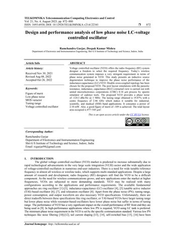
Various design flow for the LC-VCO have been proposed in the literatures [22], [26]. Design specifications originate from the application where VCO is being used. Technology file or foundry to be used is also an important criterion. Next, there is a need to identify the design variable available for the design. The important design variables are MOS transistor size, the geometrical parameter ofthe inductor, and a number of transistor arrays in the varactor. The design flowis shown in Figure 1.
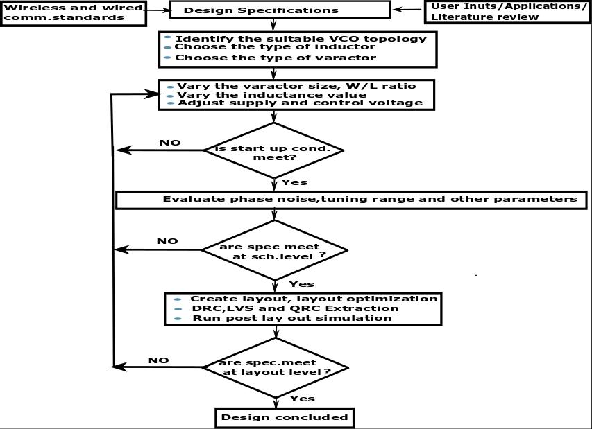
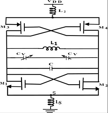
The noise associated with tank and active circuits are the intrinsic noise sources that cannot be permanently removed. Active devices contribute major noise as compared to other components of the VCO. The designers have minimal options like device selections, and setting bias operating points. To minimize the phase noise. The PN models discussed in [25], [27] gives some insights into low PN VCO design. As per the lesson’s equation [25], tank Q, active circuitry, signal power, and other frequency parameters are the important consideration for low phase noise. The flicker noise reduction mechanism was discussed in [28], [29]. Various techniques exist to reduce the phase noise performances in VCO [29], [12], [30], [31], [16] The VCO design techniques need to be investigated in several aspects to obtain a better PN performance. The tail current transistor used in conventional LC-VCO as shown in the Figure 2(a) contributes to phase noise. As reported in [12], [15], [10] noise from tail transistor can be effectively suppressed by filtering techniques. Here, we present the inductive source degeneration technique for lowphase noise VCO design.
Figure 2(a) shows the conventional design of LC-VCO while Figure 2(b) shows the proposed double CC VCO with inductive source degeneration. The advantages of these differential topologies are that they can directly drive circuits that require a differential input. The complementary cross-coupled configuration has been used to compensate losses produced by tank circuits and active sources. This complementary structure gives double transconductance compared to conventional all NMOS structure at the cost of tuning range and thus relaxes the start-up criteria. The negative resistance which is required for start-up oscillation may be expressed as:
Where �������� is the equivalent negative resistance offered by double cross-coupled transistor, ������ is the parallel resistance provided by LC tank, ������ and ������ are the transconductance of NMOS and PMOS transistor respectively.
In differential CC LC oscillator, tail current generator at source is considered the major source of flicker noise. The close-in PN is dominated by the up-converted flicker noise of the tail current [30], [32], [33]. Most of the complementary structures either use NMOS or PMOS tail current sources. In any balanced circuit, even harmonics flow in a common mode path; therefore, there is a need for high impedance to even harmonics of the oscillation frequency. The high impedance offered by the tail current source also helps to avoid the degradation of the resonator’s quality factor [12]
Source degeneration scheme is an excellent technique to suppress flicker noise up-conversion into phase noise [34]. Several circuit structures using source degeneration techniques such as inductive degenerated, resistive degenerated, capacitive degenerated, and LC filtering technique [12], [31] are presented in various research papers. By removing the tail current generator in the proposed design, the close in phase noise could be improved, but this will impair the quality factor of resonator and due to the absence of high impedance, oscillator will be more sensitive to ground noise. So, instead of tail current generator, an inductor is inserted.
In perfectly balanced LC-VCO, odd and even harmonics are present. The odd harmonics exist in a differential path with no current flowing through the tail transistor. Opposite to that, even harmonics flow from supply to ground path, including the tail transistor. The nonlinearities in the oscillator are responsible for converting low-frequency noise of the tail transistor into high-frequency noise around the even harmonics and the down-converting to the PN around the carrier. The effect of higher-order harmonics on the phase noise is neglected oweing to their low level.
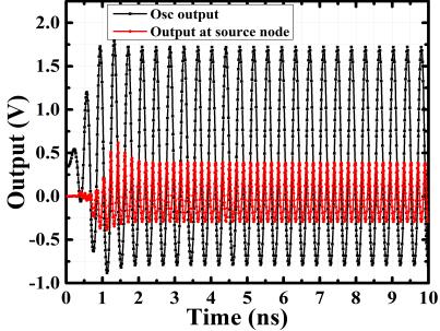
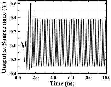
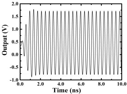
The inductor provides a high impedance common node for differential pairs at the cost of the area. A spiral inductor (����) is used to resonate in parallel with parasitic capacitance ���� at source node (��). If the value of inductor (����) is chosen in such a way that ���� (resonant frequency at source node) is equal to the second harmonic frequency (2����) of the oscillator, then impedance (����) at source node seen from differential transistor is approximately infinite [35]. The Resonant frequency at output node is depicted in Figure 3(a). The Resonant frequency at source node (��) as shown in Figure 3(b) and Figure 3(c) is:
Where ���� is the resonant frequency at source node, ���� is the series inductor and ���� is the total capacitance at the source terminal (��) of the oscillator including parasitic capacitance and source capacitance of NMOS transistors. This can be shown:
It can been seen from (8), as ���� (Figure 3(b)) is approximately equal to second harmonic of oscillator frequency (����) (Figure 3(a)), the impedance ���� at source node approaches infinity, and the �� of the inductance-capacitance tank is maintained. A symmetrical waveform is also helpful to get the lower PN [36] So in the proposed design, ��/�� ratio of tramsostors of CC is chosen to have equal rise and fall time in the waveform. To obtain symmetrical waveform, the transconductance of PMOS and NMOS transistors should be equal. This leads to (9):
Where ���� and ���� are the surface mobilities of NMOS and PMOS channel respectively, ������ is the capacitance per unit area of the gate oxide, ���� ���� and ���� ���� are the effective channel width-length ratio of PMOS and NMOS device respectively
(a)
(b)
(c)
Figure 3. Simulated waveform: (a) single-ended output signal (����), (b) second harmonic of oscillating frequency (2����) at source node (��), and (c) at the source and output node
The higher sensitivity of the oscillating frequency to voltage supply (frequency pushing) can be lowered by inserting an inductor (��2) having 3.5 nH inductance between a supply voltage and resonator. In addition to that, it also provides a high impedance path between resonant tank and power supply (������). Variation in the oscillation frequency has been obtained by varying the control voltage of IMOS varactor consisting of 5 parallel units of two series connected backto backPMOS transistor.
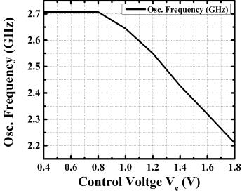
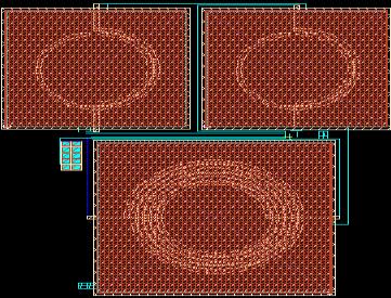
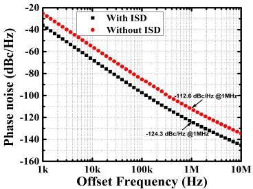
The performance of the design is greatly affected by the parasitic resistance and capacitance present in the layout. The good layout design considerably reduces the degrading of the system performance. The complete layout of the proposed inductive source degeneration-based LC-VCO is drawn using Cadence Virtuoso layout suite XL with UMC process parameter as shown in Figure 4. It consists of three spiral inductor, a varactor bank, and CC pairs of the transistor. The spiral inductors occupy the 99% area in the layout. The total area is 477 µm × 545 µm. After design rule check (DRC) and layout versus schemetic (LVS), quantus parasitic extraction was performed to extract the parasitics offered by the design. The dimensions and values of the transistor are given in Table 2. Post layout simulation from the extracted cell view is required to evaluate the effect of parasitic on the system’s performance. This also helps a designer to get the results closer to reality. Here in this work, post layout simulations were carried out with UMC 0.18 µm process by spectre simulator of cadence tools. The periodic steady state (PSS) simulation is performed to evaluate the tuning range of the proposed VCO. IMOS varactor consisting of PMOS transistors has been used to regulate the tuning range. The VCO exhibits a turning range from 2.22 GHz to 2.71 GHz when the control voltage varies from 0.8 V to 1.8 V, as shown in Figure 5. Phase noise performance represents the spectral purity of the output signal. The plot shown in Figure 6 shows the single sideband PN with respect to relative frequency from the carrier for the proposed and conventional design.
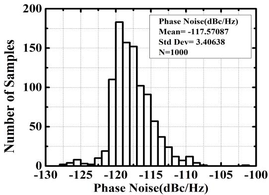
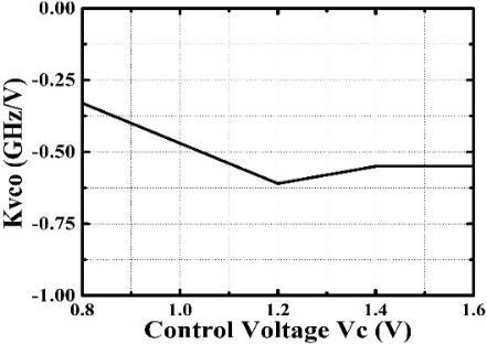
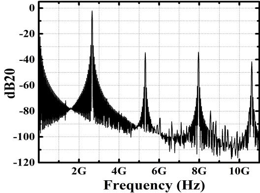
At offset frequency of 1 MHz, the PN achieved for this technique is -124.3 dBc/Hz, which can meet the specification of ISM band applications. Using the proposed technique, PN improvement of -11.7 dBc/Hz at a frequency offset of 1 MHz is achieved compared to the conventional design. A buffer amplifier is not considered in the design but output power must have a reasonable value. The output spectrum is shown in Figure 7. The VCO gain (��������) with respected to tuning voltage is ploted in Figure 8. The Monte Carlo (MC) simulation for 1000 sample has been performed to examine the effect of process variation on the phase noise. The MC simulation based histogram is ploted in Figure 9 The VCO draws a current of 1.166 mA from the supply voltage of 1.8 V. The performance of VCO may be evaluated in terms of various specifications like PN, power dissipation, output amplitude, and tuning range. There are several figure of merits (FOMs) to evaluate the performance metrics of a VCO. The following equation is widely used to evaluate the performance of VCO [37]
Where ��(��������) represents the PN at offset frequency and ������ is the power consumption in mW. The comparison performance of the proposed works with other state of work is given in Table 3.
In this paper, the proposed design of LC-VCO was discussed with a focus on phase noise performance. The basic step in the design of VCO is the selection of a suitable topology. The design methodology for VCO was presented. The design, implementation, and layout of CMOS LC-VCOs were accomplished using Virtuoso analog design environment with UMC process parameter, and post layout simulations were performed using spectre. The low phase noise technique, namely inductive source degeneration were investigated. With low phase noise ISD, satisfactory performance of the VCO with phase noise of -124.3 dBc/Hz at 1 MHz offset frequency was obtained. The post layout simulation results confirm that these VCOs can meet the specification for applications in the 2.2 GHz to 2.7 GHz unlicensed ISM bands. The performance outcomes validate the effectiveness of the topologies and methodologies used in the design
Authors extend thanks to SMDP-C2SD (A Project of Ministry of Electronics and Information Technology, Govtorment of India) for providing VLSI-Electronic Design Automation tools in the laborotary.
[1] K. Das, N. Pradhan, V. Kumar, and S. K. Jana, “Comparison and Performance Analysis of Ring Oscillators and Current-Starved VCO in 180-nm CMOS Technology,” in 2020 International Symposium on Devices, Circuits and Systems (ISDCS), 2020, pp. 1-4, doi: 10.1109/ISDCS49393.2020.9263006.
[2] E. Zafarkhah, M. M -Nejad, and M. Zare, “Single-ended ring oscillators: analysis and design,” IET Circuits, Devices & Systems, vol. 14, no. 6, pp. 869–875, 2020, doi: 10.1049/iet-cds.2019.0190.
[3] N. Fioravanti et al., “Fabrication of ring oscillators using organic molecules of phenacene and perylenedicarboximide,” RSC Advances, vol. 11, no. 13, pp. 7538–7551, 2021, doi: 10.1039/D1RA00511A.
[4] F. Ullah, Y. Liu, Z. Li, X. Wang, M. M. Sarfraz, and H. Zhang, “A bandwidth-enhanced differential LC-voltage controlled oscillator (LC-VCO) and superharmonic coupled quadrature VCO for K-band applications,” Electronics, vol. 7, no. 8, 2018, doi: 10.3390/electronics7080127.
[5] K. A. Karthigeyan and S. Radha, “Single Event Transient study on PMOS-NMOS cross-coupled LC-VCO using PLL,” International Journal of Electronics, vol. 108, no. 3, pp. 378-394, 2021, doi: 10.1080/00207217.2020.1793419.
[6] R. C. Gurjar and D. K. Mishra, “Design and performance analysis of CMOS tunable active inductor based voltage controlled oscillator,” International Journal of Electronics, vol. 109, no. 6, pp. 915-934, 2022, doi: 10.1080/00207217.2021.1941297.
[7] O. Faruqe and M. T. Amin, “Design and Performance Analysis of Active Inductor Based VCO for IEEE 802.11a/b/g/n/ac Applications,” International Journal of Electronics, vol. 107, no. 3, pp. 494–511, 2020, doi: 10.1080/00207217.2019.1661030.
[8] T. Onomi, “Experimental Demonstration and Performance Estimation of a new Relaxation Oscillator Using a Superconducting Schmitt Trigger Inverter,” Physics Procedia, vol. 81, pp. 141–144, 2016, doi: 10.1016/j.phpro.2016.04.030.
[9] J. B. Scott, Analog electronic design : principles and practice of creative design Sydney: Prentice Hall, 1992. [Online]. Available: https://catalogue.nla.gov.au/Record/3002579
[10] S. -Y. Lee, B. Shrestha, and N. -Y. Kim, “Analysis of two filtering techniques in differential LC VCO design using asymmetric tank structure,” IETE Journal of Research, vol. 54, no. 6, pp. 386–390, 2008. [Online]. Available: https://www.tandfonline.com/doi/abs/10.4103/0377-2063.48619
[11] X. Wang, X. Yang, X. Xu, and T. Yoshimasu, “2.4-GHz-band low-voltage LC-VCO IC with simplified noise filtering in 180-nm CMOS,” in 2016 IEEE MTT-S International Wireless Symposium (IWS), 2016, pp. 1-3 doi: 10.1109/IEEE-IWS.2016.7585430.
[12] E. Hegazi, H. Sjöland, and A. A. Abidi, “A filtering technique to lower LC oscillator phase noise,” IEEE Journal of Solid-State Circuits, vol. 36, no. 12, pp. 1921–1930, 2001, doi: 10.1109/4.972142.
[13] P. Shasidharan, H. Ramiah, and J. Rajendran, “A 2.2 to 2.9 GHz Complementary Class-C VCO with PMOS Tail-Current Source Feedback Achieving-120 dBc/Hz PN at 1 MHz Offset,” IEEE Access, vol. 7, pp. 91325-91336, 2019, doi: 10.1109/ACCESS.2019.2927031.
[14] B. Jafari and S. Sheikhaei, “Low phase noise LC VCO with sinusoidal tail current shaping using cascode current source,” AEUInternational Journal of Electronics and Communications, vol. 83, pp. 114–122, 2018, doi: 10.1016/j.aeue.2017.08.032.
[15] Z. Zong, G. Mangraviti, and P. Wambacq, “Low 1/f3 Noise Corner LC-VCO Design Using Flicker Noise Filtering Technique in 22nm FD-SOI,” IEEE Transactions on Circuits and Systems I: Regular Papers, vol. 67, no. 5, pp. 1469-1480, 2020, doi: 10.1109/TCSI.2020.2970267.
[16] N. Chen, S. Diao, L. Huang, and F. Lin, “Reduction of 1/f 3 phase noise in LC oscillator with improved self-switched biasing,” Analog Integrated Circuits and Signal Processing, vol. 84, pp. 19–27, 2015, doi: 10.1007/s10470-015-0560-9.
[17] I. Ghorbel, F. Haddad, and W. Rahajandraibe, “Ultra low power RF cross-coupled VCO design in the subthreshold regime with high immunity to PVT variations in 130nm CMOS technology,” 2015 IEEE 13th International New Circuits and Systems Conference (NEWCAS), 2015, pp. 1-4, doi: 10.1109/NEWCAS.2015.7182034.
[18] I. Ghorbel, F. Haddad, W. Rahajandraibe, and M. Loulou, “Design Methodology of Ultra-Low-Power LC-VCOs for IoT Applications,” Journal of Circuits, Systems and Computers, vol. 28, no. 7, 2019, doi: 10.1142/S0218126619501226.
[19] C. -Y. Lin, Y. -K. Lin, P. -Z. Rao, J. -H. Tarng, and S. -J. Chung, “A low-power low-voltage current-reused voltage-controlled oscillator with amplitude-balanced technique,” 2017 Progress in Electromagnetics Research Symposium - Fall (PIERS - FALL), 2017, pp. 3011-3015, doi: 10.1109/PIERS-FALL.2017.8293650
[20] M. -T. Hsu, T. -H. Han, and Y. -Y. Lee, “Design of Sub-1 mW CMOS LC VCO based on current reused topology with Qenhancement and body-biased technique,” Microelectronics Journal, vol. 45, no. 6, pp. 627–633, 2014, doi: 10.1016/j.mejo.2014.04.011.
[21] B. Sadhu, T. Anand, and S. K. Reynolds, “A Fully Decoupled LC Tank VCO Topology for Amplitude Boosted Low Phase Noise Operation,” IEEE Journal of Solid-State Circuits, vol. 53, no. 9, pp. 2488–2499, 2018, doi: 10.1109/JSSC.2018.2859787.
[22] I. Ghorbel, F. Haddad, W. Rahajandraibe, and M Loulou, “Ultra-low-power wideband NMOS LC-VCO design for autonomous connected objects,” Analog Integrated CircuitsandSignal Processing,vol.106,pp.375–383,2021,doi:10.1007/s10470-020-01613-0.
[23] A. Hajimiri and T. H. Lee, “Design issues in CMOS differential LC oscillators,” IEEE Journal of Solid-State Circuits, vol. 34, no. 5, pp. 717-724, 1999, doi: 10.1109/4.760384.
[24] A. Fard, T. Johnson, M. Linder, and D. Aberg, “A comparative study of CMOS LC VCO topologies for wide-band multi-standard transceivers,” in The 2004 47th Midwest Symposium on Circuits and Systems, 2004. MWSCAS '04, 2004, doi: 10.1109/MWSCAS.2004.1354280.
[25] D. B. Leeson, “A Simple Model of Feedback Oscillator Noise Spectrum,” in Proc. of the IEEE, 1966, vol. 54, no. 2, pp. 329–330, 1966, doi: 10.1109/PROC.1966.4682.
[26] R. Fiorelli, E. J. Peralías, and F. Silveira, “LC-VCO design optimization methodology based on the gm/ID ratio for NM CMOS technologies,” IEEE Transactions on Microwave Theory and Techniques, vol. 59, no. 7, pp. 1822–1831, 2011, doi: 10.1109/TMTT.2011.2132735.
[27] A. Hajimiri and T. H. Lee, “A General Theory of Phase Noise in Electrical Oscillators,” IEEE Journal of Solid-State Circuits, vol. 33, no. 2, pp. 179-194, 1998, doi: 10.1109/4.658619.
[28] Y. Hu, T. Siriburanon, and R. B. Staszewski, “Oscillator flicker phase noise: A tutorial,” IEEE Transactions on Circuits and Systems II: Express Briefs, vol. 68, no. 2, pp. 538-544, 2021, doi: 10.1109/TCSII.2020.3043165.
[29] J. Mazloum and S. Sheikhaei, “1/f3 (Close-in) Phase Noise Reduction by Tail Transistor Flicker Noise Suppression Technique,” Journal of Circuits, Systems and Computers, vol. 29, no. 3, 2020, doi: 10.1142/S0218126620500358.
[30] B. De Muer, M. Borremans, M. Steyaert, and G. L. Puma, “2-GHz LPN integrated LC-VCO set with flicker-noise upconversion minimization,” IEEE Journal of Solid-State Circuits, vol. 35, no. 7, pp. 1034–1038, 2000, doi: 10.1109/4.848213.
[31] P. Andreani and H. Sjöland, “A 1.8 GHz CMOS VCO with reduced phase noise,” in 2001 Symposium on VLSI Circuits. Digest of Technical Papers (IEEE Cat. No.01CH37185), 2001, pp. 121-122, doi: 10.1109/VLSIC.2001.934213.
[32] D. Ham and A. Hajimiri, “Concepts and methods in optimization of integrated LC VCOs,” IEEE Journal of Solid-State Circuits,
880
vol. 36, no. 6, pp. 896–909, 2001, doi: 10.1109/4.924852.
ISSN: 1693-6930
[33] J. J. Rael and A. A. Abidi, “Physical processes of phase noise in differential LC oscillators,” in Proc. of the IEEE 2000 Custom Integrated Circuits Conference (Cat. No.00CH37044), 2000, pp. 569-572, doi: 10.1109/CICC.2000.852732.
[34] Y. Ying, L. Huang, L. Cai, and F. Lin, “A 4.89-GHz low-phase-noise VCO in CMOS technology,” in 2012 IEEE International Symposium on Radio-Frequency Integration Technology (RFIT), 2012, pp. 198-200, doi: 10.1109/RFIT.2012.6401659.
[35] T. Wu, U. -K. Moon, and K. Mayaram, “Dependence of LC VCO oscillation frequency on bias current,” in 2006 IEEE International Symposium on Circuits and Systems (ISCAS), 2006, doi: 10.1109/ISCAS.2006.1693764.
[36] Y. -H. Kao and M. -T. Hsu, “Theoretical analysis of low phase noise design of CMOS VCO,” IEEE Microwave and Wireless Components Letters, vol. 15, no. 1, pp. 33–35, 2005, doi: 10.1109/LMWC.2004.840974.
[37] P. Kinget, “Integrated GHz Voltage Controlled Oscillators,” in Analog Circuit Design, Boston, MA: Springer, 1999, pp. 353–381, doi: 10.1007/978-1-4757-3047-0_17.
[38] D. Sachan, H. Kumar, M. Goswami, and P. K. Misra, “A 2.4 GHz Low Power LPN Enhanced FOM VCO for RF Applications Using 180 nm CMOS Technology” Wireless Personal Communications, vol. 101, pp. 391–403, 2018, doi: 10.1007/s11277-018-5695-4.
[39] S. R. A Rahman, S. H. M Ali, N. Kamal, A. A. Ahmad, and M. Othman, “Design of 2.4 GHz CMOS LC tank voltage controlled oscillator (VCO) for PLL using 0.18 μm CMOS technology,” in 2018 IEEE International Conference on Semiconductor Electronics (ICSE), 2018, pp. 246-249, doi: 10.1109/SMELEC.2018.8481242.
Ramchandra Gurjar received the B.E. in Electronics and Communication Engineering and M.E. in Digitial Technique Instrumentation from Rajiv Gandhi Technological University, Bhopal (India) in year 2001 and 2006, respectively. He obtained his Ph.D. in Electronics Engineering from RGPV, Bhopal. He is currently associate professor in SGSITS, Indore (India). His current research interests include design of active inductor, VCO, PLLs and FPGA based design. He can be contacted at email: rcgurjar94@gmail.com.
Deepak Kumar Mishra received the B.E. degree in Electronics and M.E. in Applied Electronics and Servomechanism from the DAVV (Formerly- University of Indore) Indore in 1979 and 1984 respectively. He obtained his Ph.D. from DAVV, Indore (India). He is currently professor in SGSITS Indore. His research area includes the design, development and testing of microprocessor and microcomputer based electronic instrumentation, RF IC design, analog and mixed signal VLSI circuit design, dynamic testing of high speed A/D converters, low power VLSI design, and system on chip design for biomedical signal processing. He can be contacted at email: mishradrc@gmail.com, dmishra@sgsits.ac.in.

TELKOMNIKA Telecommun Comput El Control, Vol. 21, No. 4, August 2023: 872-880