SOLUTIONMANUAL


Columbus, Ohio

Copyright © 2009 by Pearson Education, Inc., Upper Saddle River, New Jersey 07458.
Pearson Prentice Hall. All rights reserved. Printed in the United States of America. This publication is protected by Copyright and permission should be obtained from the publisher prior to any prohibited reproduction, storage in a retrieval system, or transmission in any form or by any means, electronic, mechanical, photocopying, recording, or likewise. For information regarding permission(s), write to: Rights and Permissions Department.
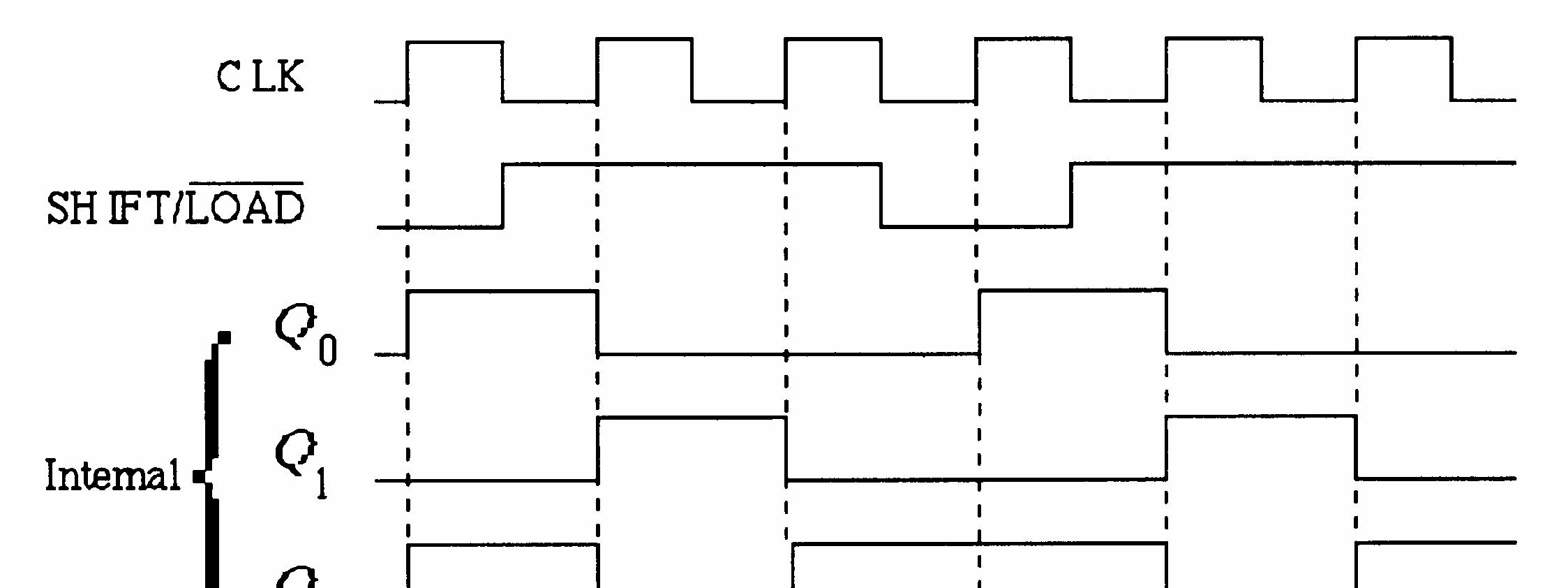
Pearson Prentice Hall™ is a trademark of Pearson Education, Inc.
Pearson® is a registered trademark of Pearson plc
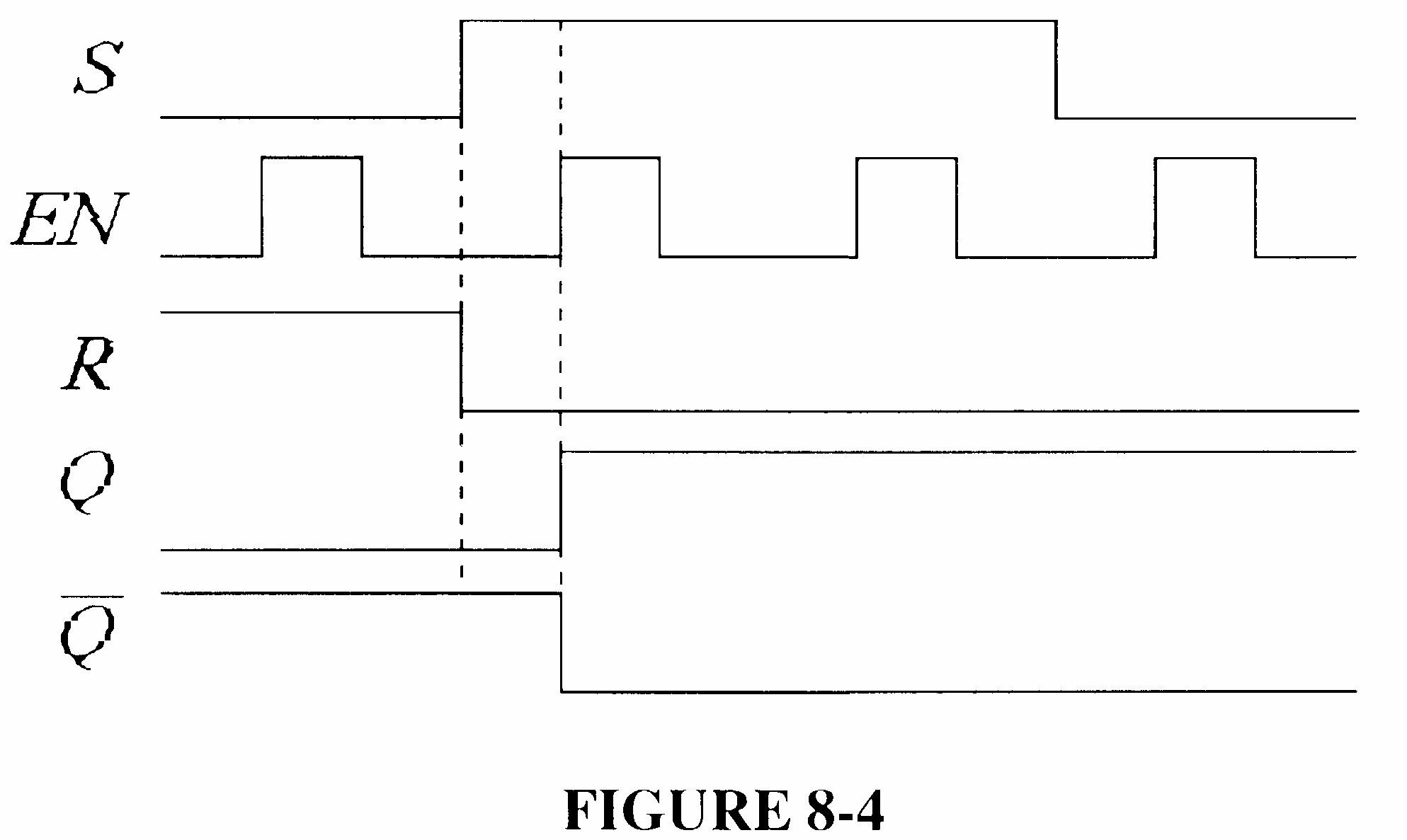
Prentice Hall® is a registered trademark of Pearson Education, Inc.
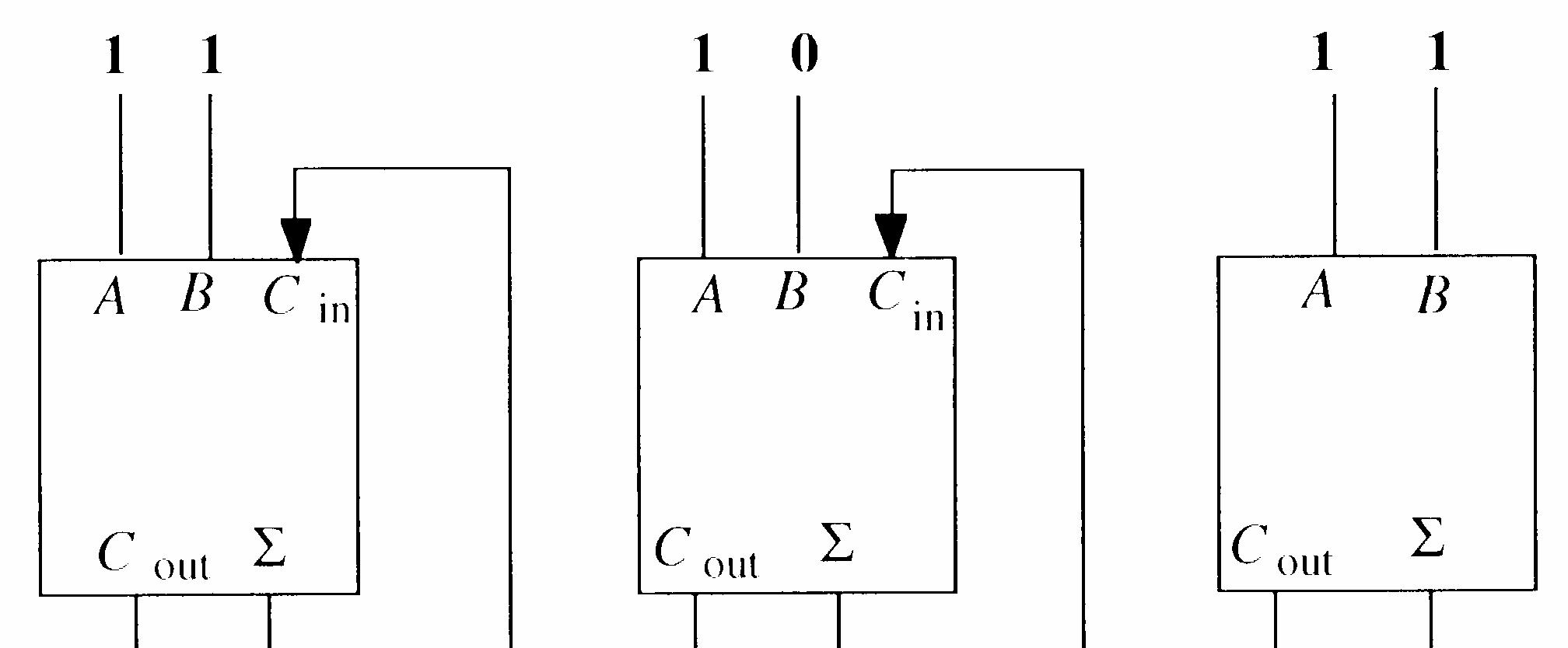
Instructors of classes using Floyd, Digital Fundamentals, Tenth Edition , may reproduce material from the instructor’s manual for classroom use. 10 9 8 7 6 5 4 3 2 1

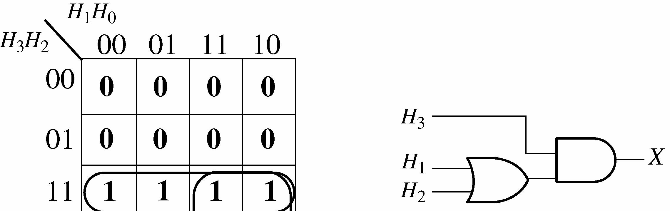
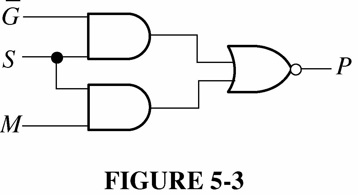
ISBN-13: 978-0-13-712960-7
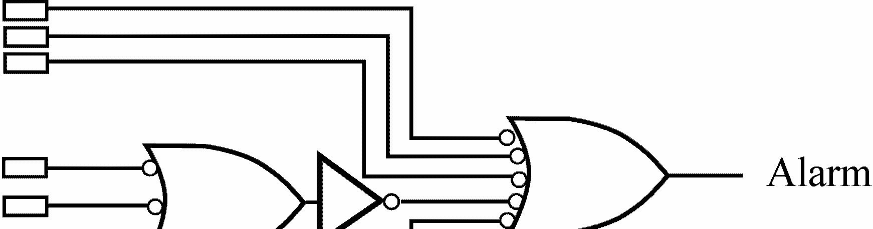
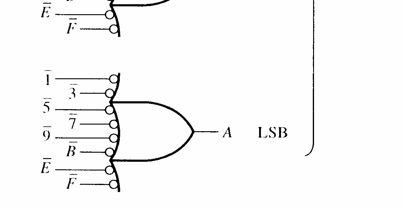
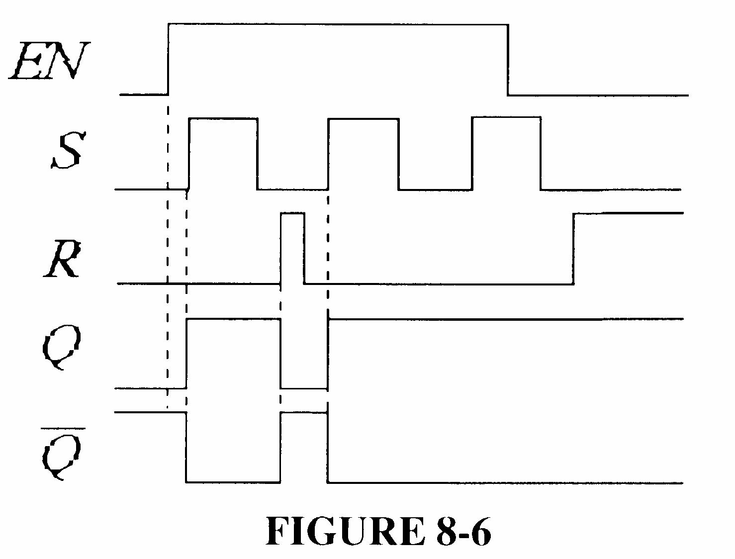
ISBN-10: 0-13-712960-2
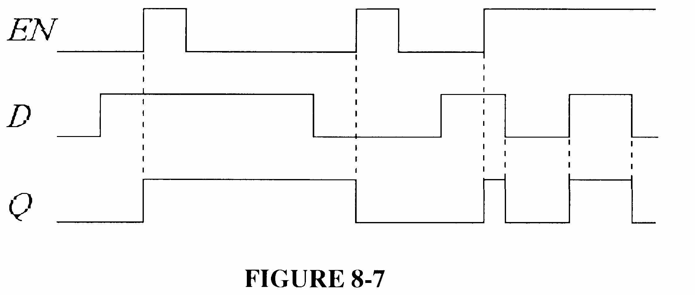
To access supplementary materials online, instructors need to request an instructor access code. Go to www.pearsonhighered.com/irc, where you can register for an access code. Within 48 hours after registering you will receive a confirming e-mail including an instructor access code. Once you have received your code, go the site and log on for full instructions on downloading the materials you wish to use.
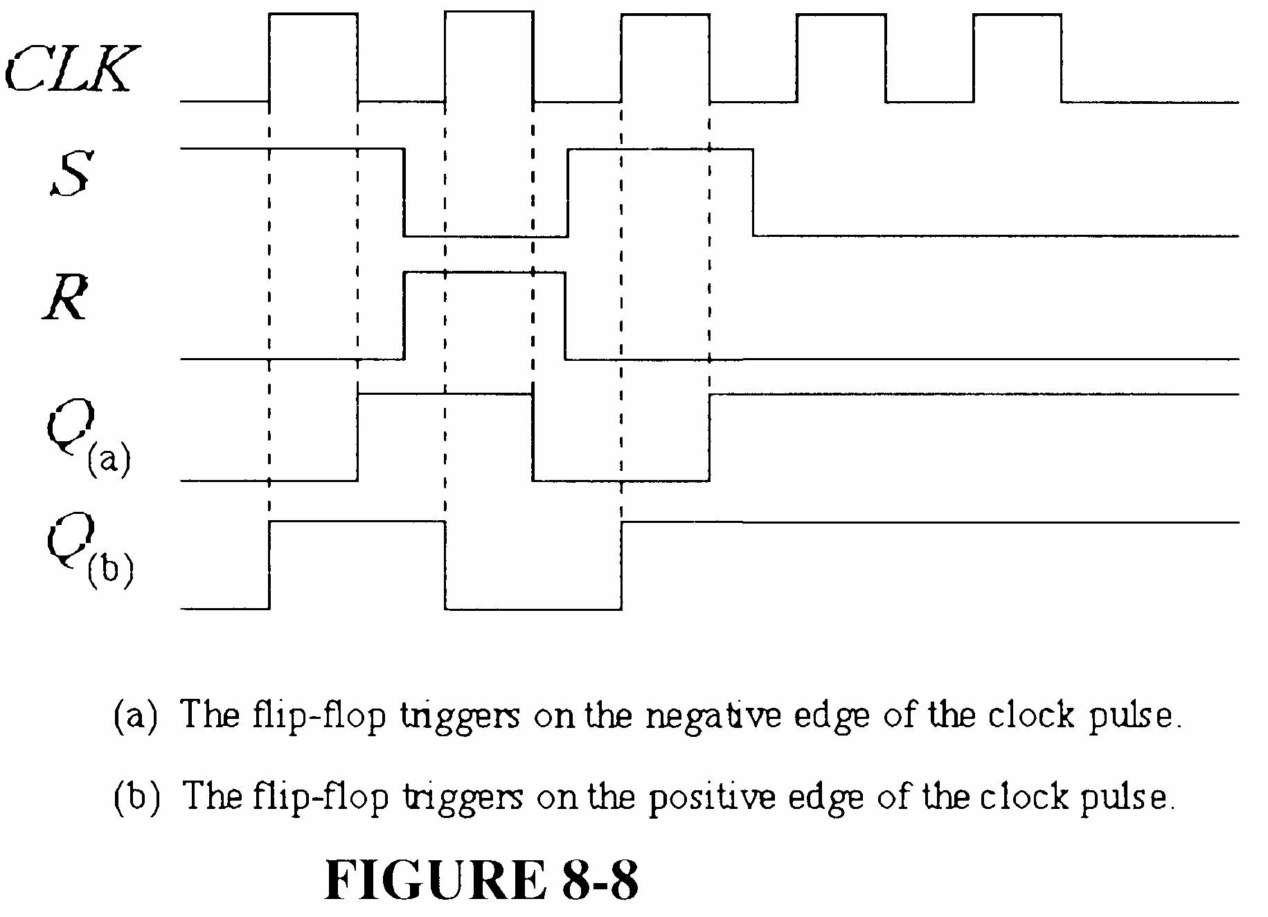
NOTE: For access to hidden faults in Multisim circuits, the password is book
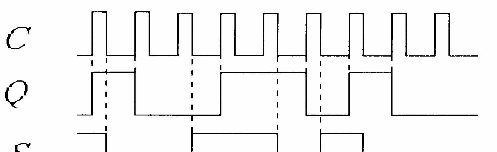
1. Digital data can be transmitted and stored more efficiently and reliably than analog data. Also, digital circuits are simpler to implement and there is a greater immunity to noisy environments.
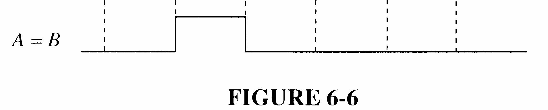
2. Pressure is an analog quantity.
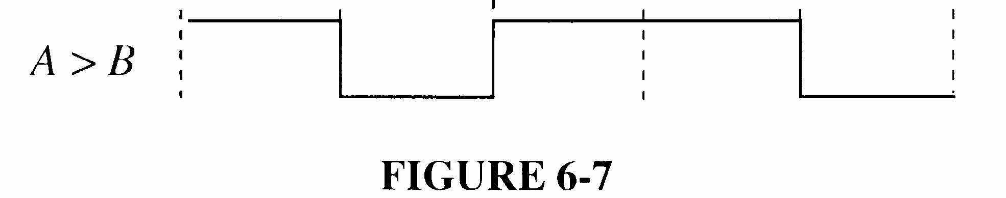
3. A clock, a thermometer, and a speedometer can have either an analog or a digital output.
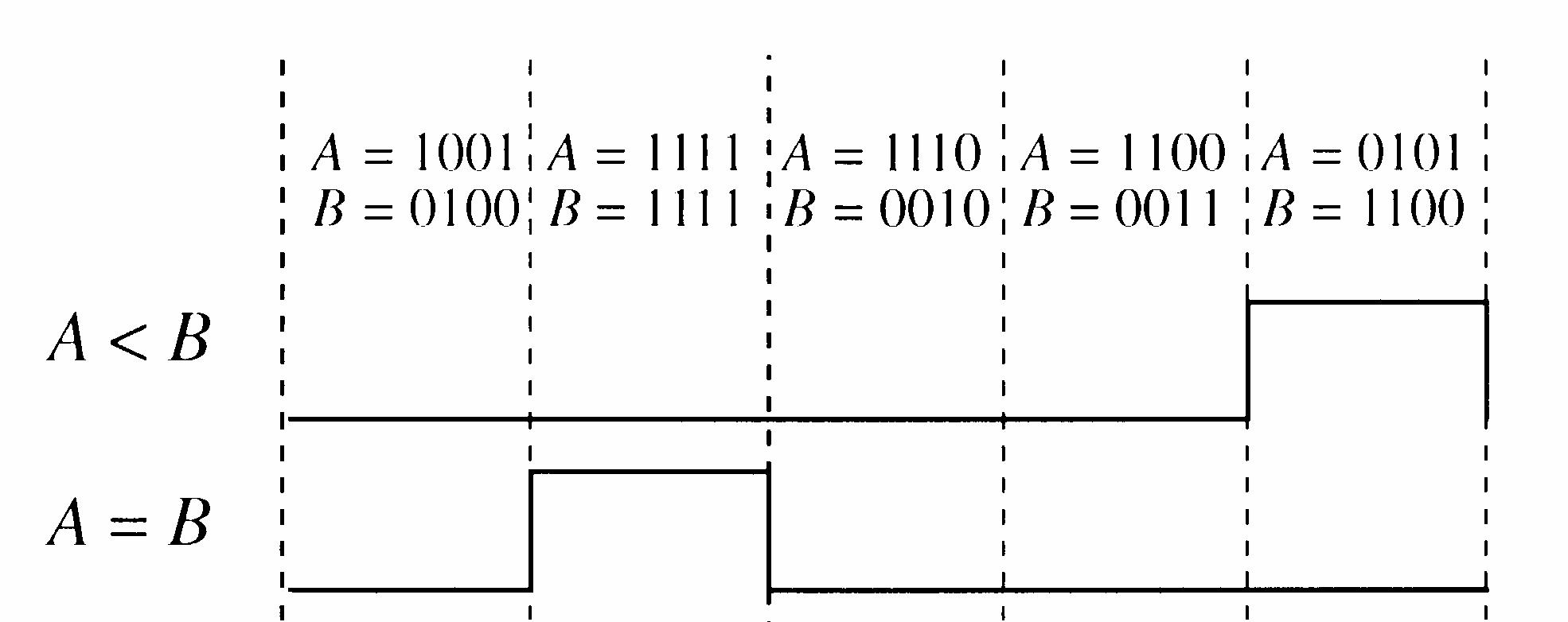
4. In positive logic, a 1 is represented by a HIGH level and a 0 by a LOW level. In negative logic, a 1 is represented by a LOW level, and a 0 by a HIGH level.
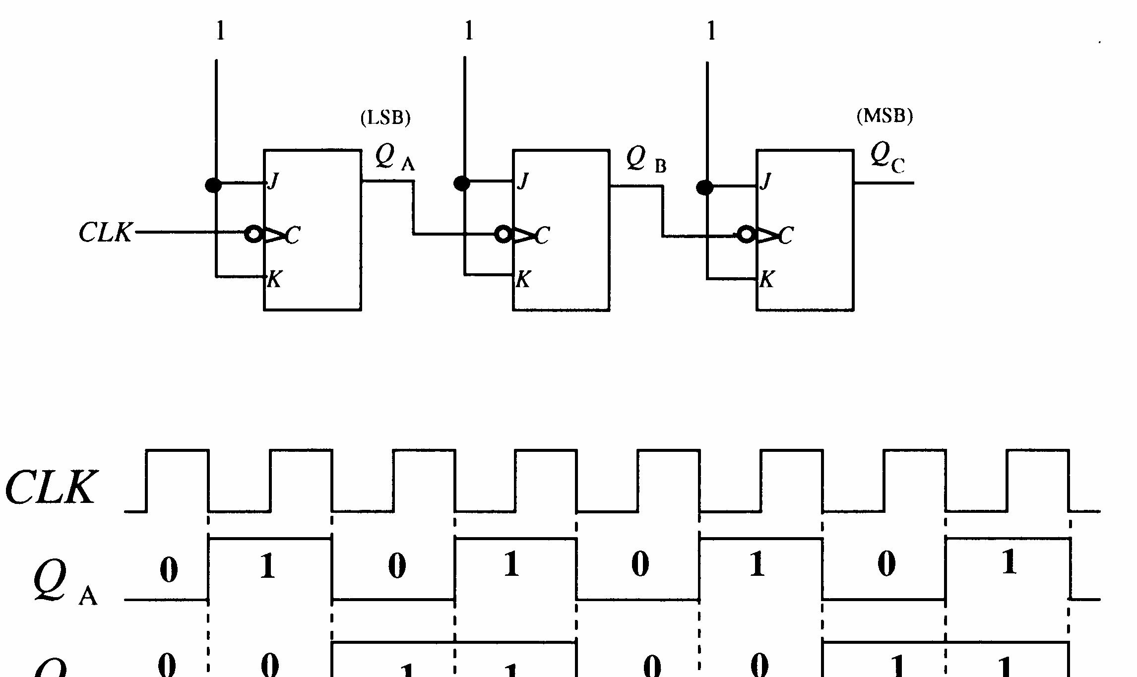
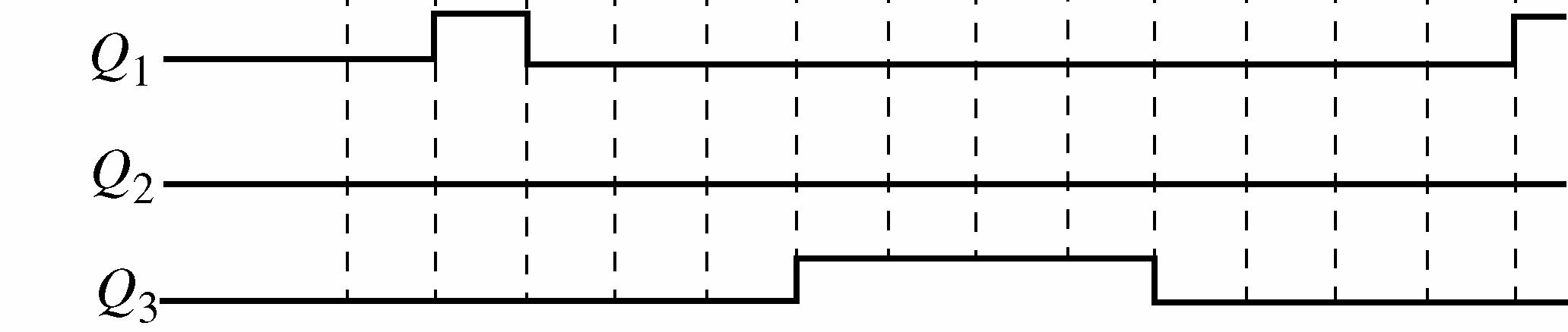
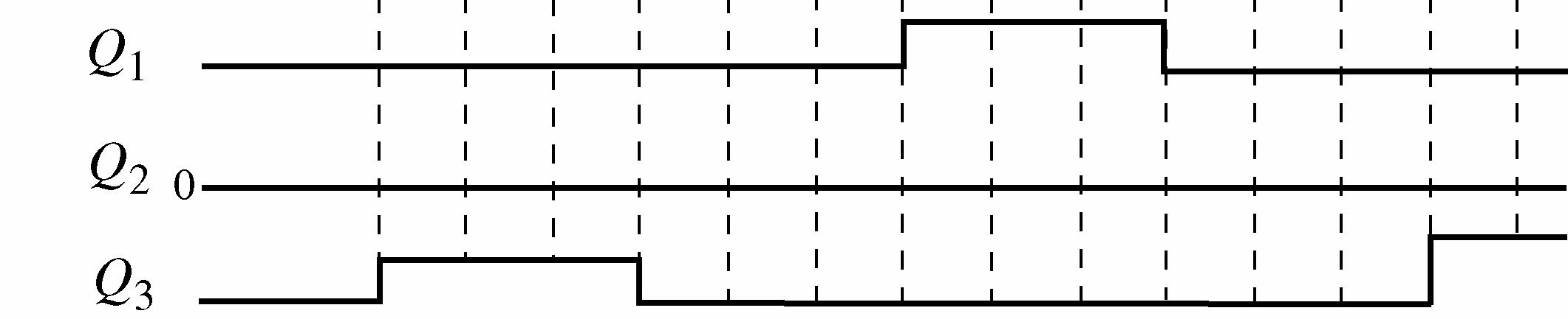
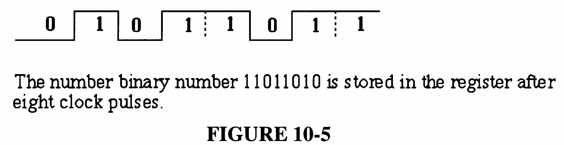
5. HIGH = 1; LOW = 0. See Figure 1-1.
6. A 1 is a HIGH and a 0 is a LOW:
(a) HIGH, LOW, HIGH, HIGH, HIGH, LOW, HIGH
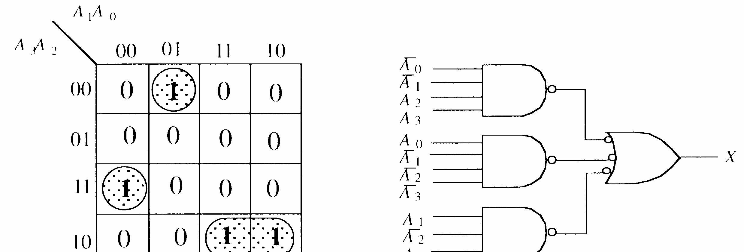
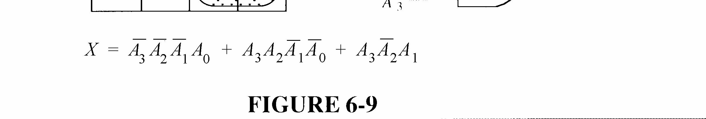
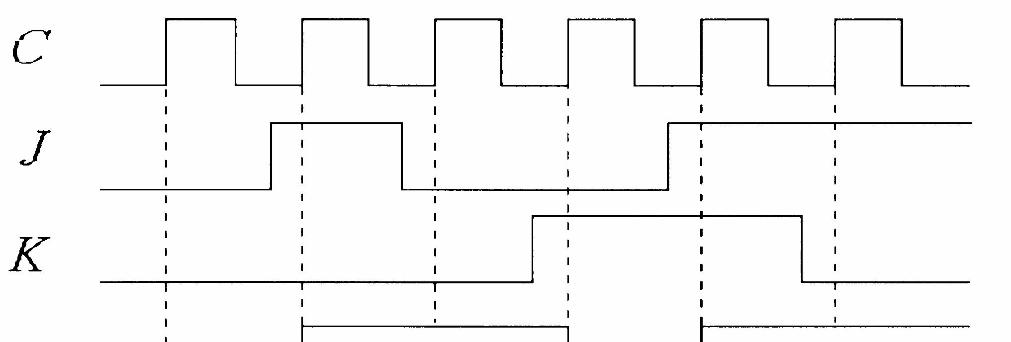
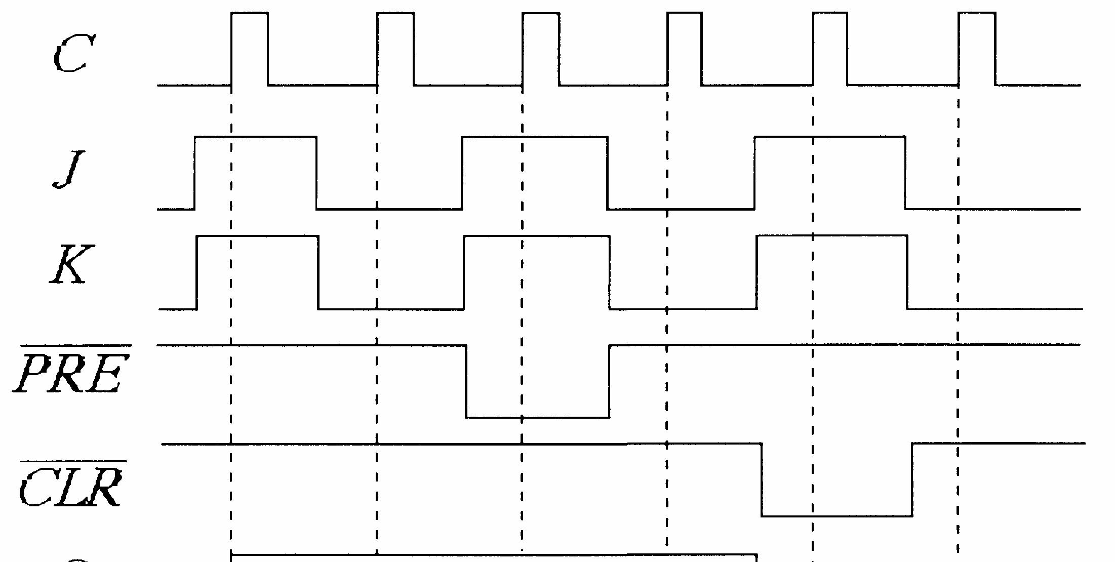
(b) HIGH, HIGH, HIGH, LOW, HIGH, LOW, LOW, HIGH
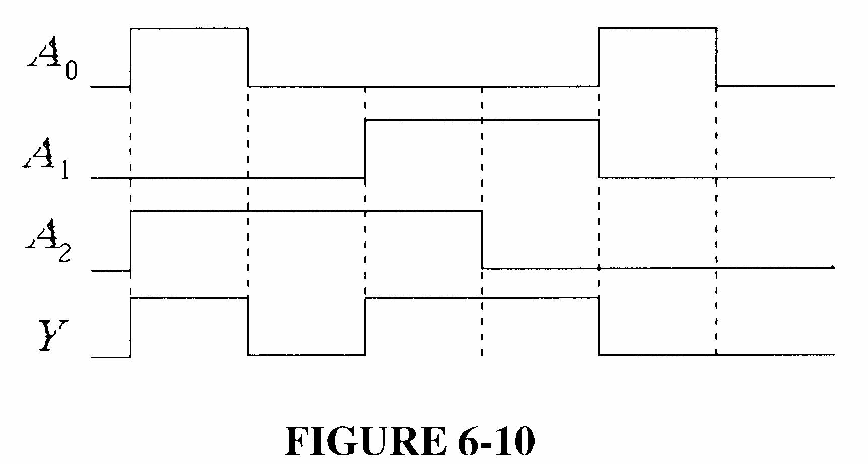
7. See Figure 1-2.

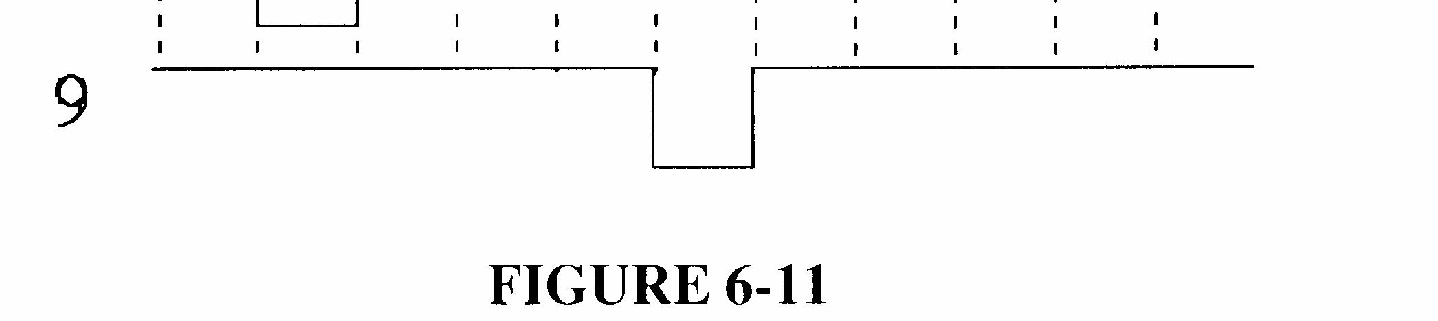
8. T = 4 ms. See Figure 1-3.
9. f = ms 4 1 1 = T = 0.25 kHz = 250 Hz
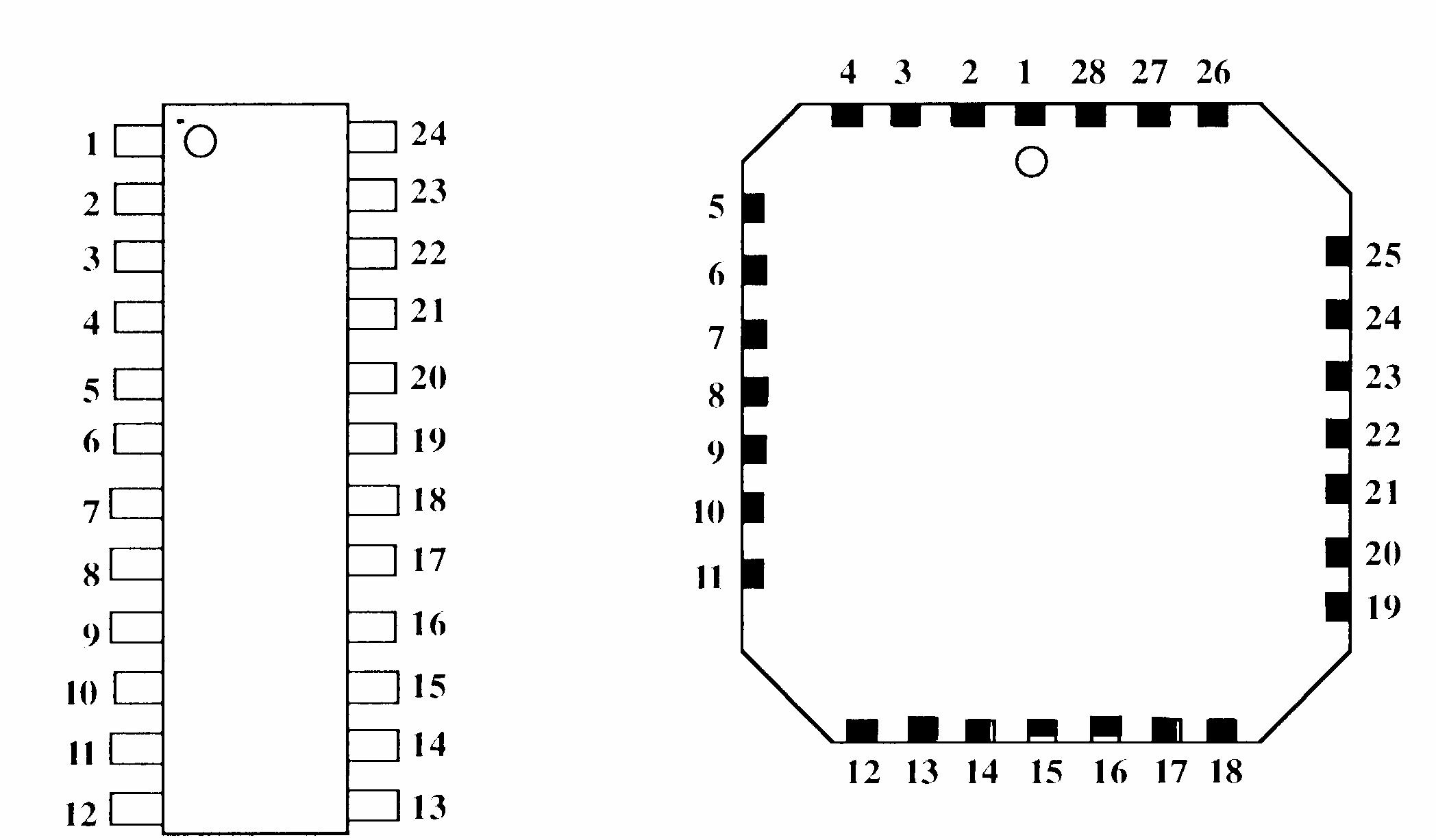
10. The waveform in Figure 1-61 is periodic because it repeats at a fixed interval.
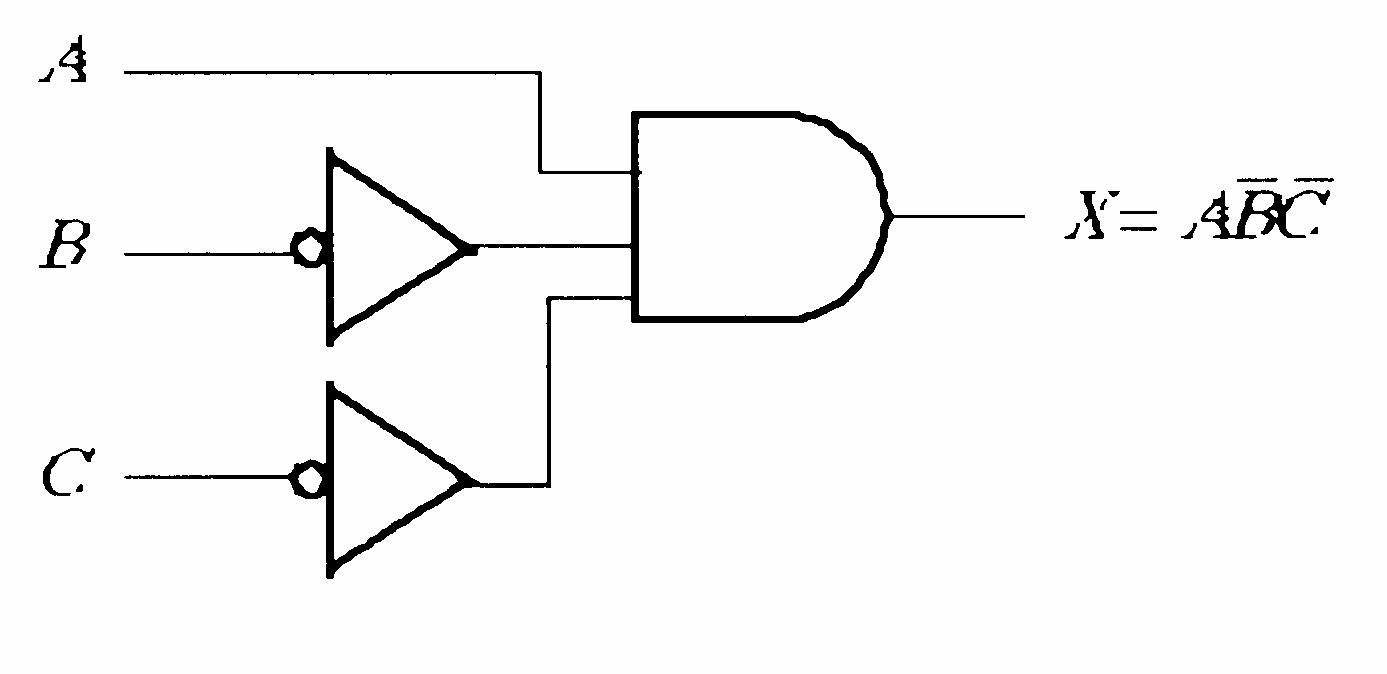
11. tW = 2 ms; T = 4 ms % duty cycle =
12. See Figure 1-4.
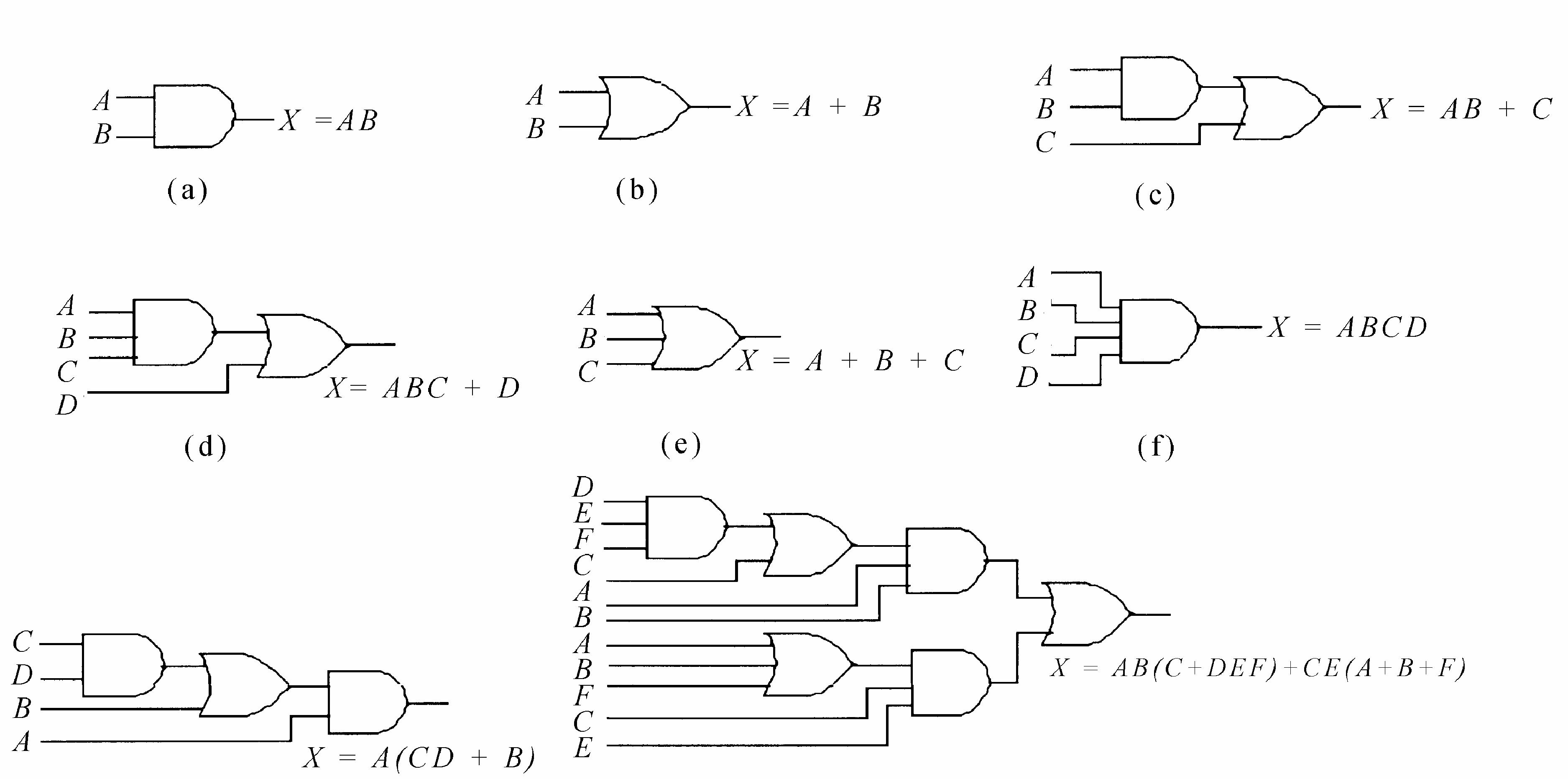
13. Each bit time = 1 μs
Serial transfer time = (8 bits)(1 μs/bit) = 8 μs
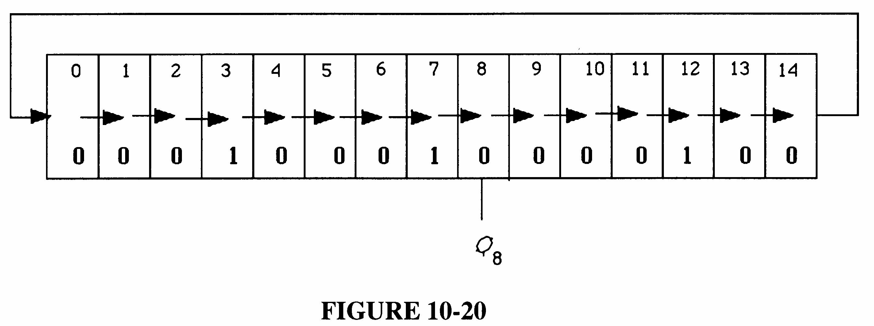
Parallel transfer time = 1 bit time = 1 μs
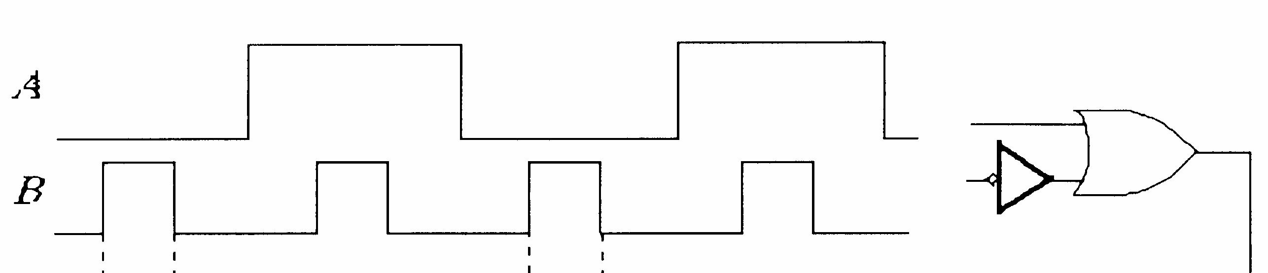
14. T = 11 3.5 GHz f = = 0.286 ns
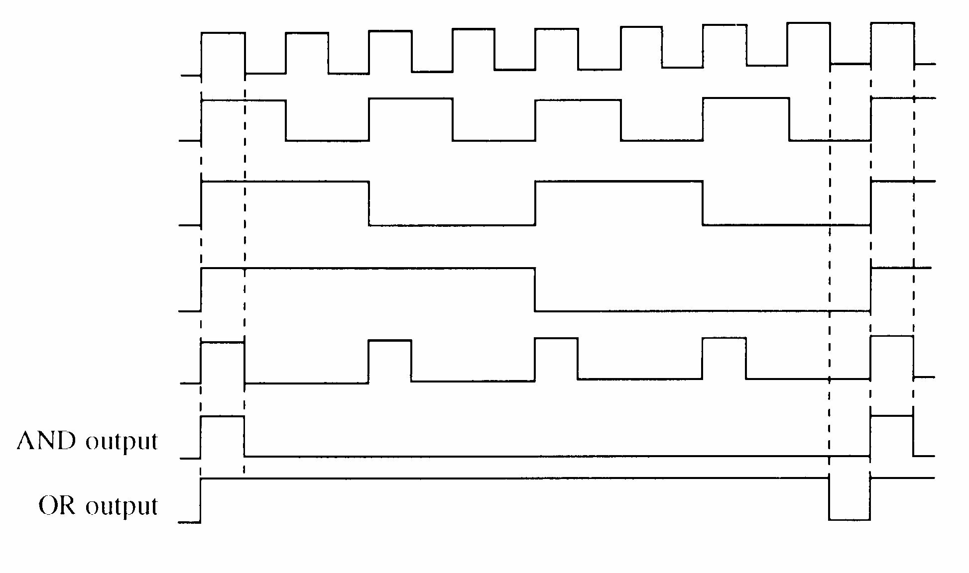
15. LON = SW1 + SW2 + SW1 SW2
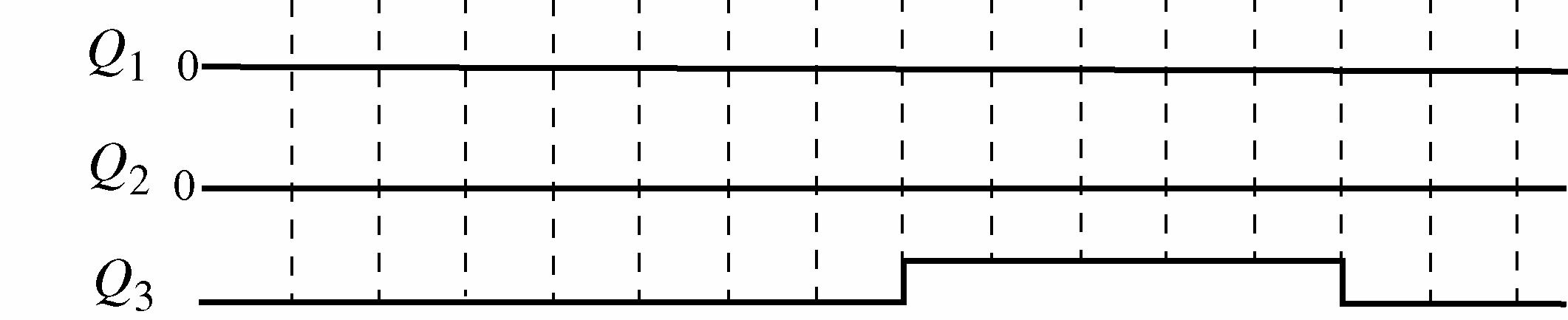
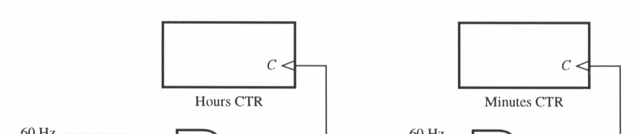
16. An AND gate produces a HIGH output only when all of its inputs are HIGH.
17. AND gate. See Figure 1-5.
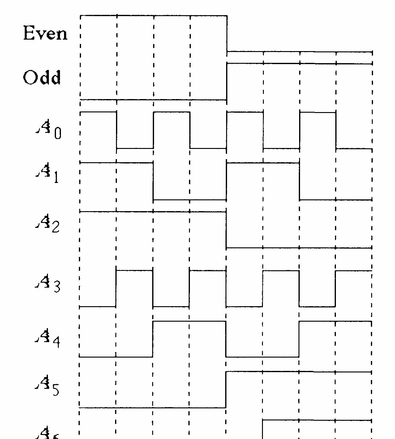
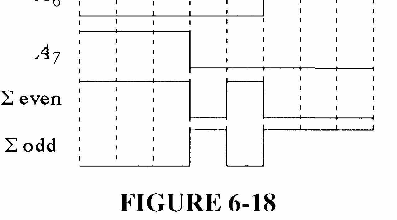
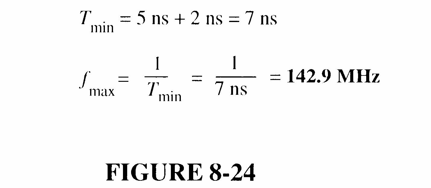
18. An OR gate produces a HIGH output when either or both inputs are HIGH. An exclusive-OR gate produces a HIGH if one input is HIGH and the other LOW.
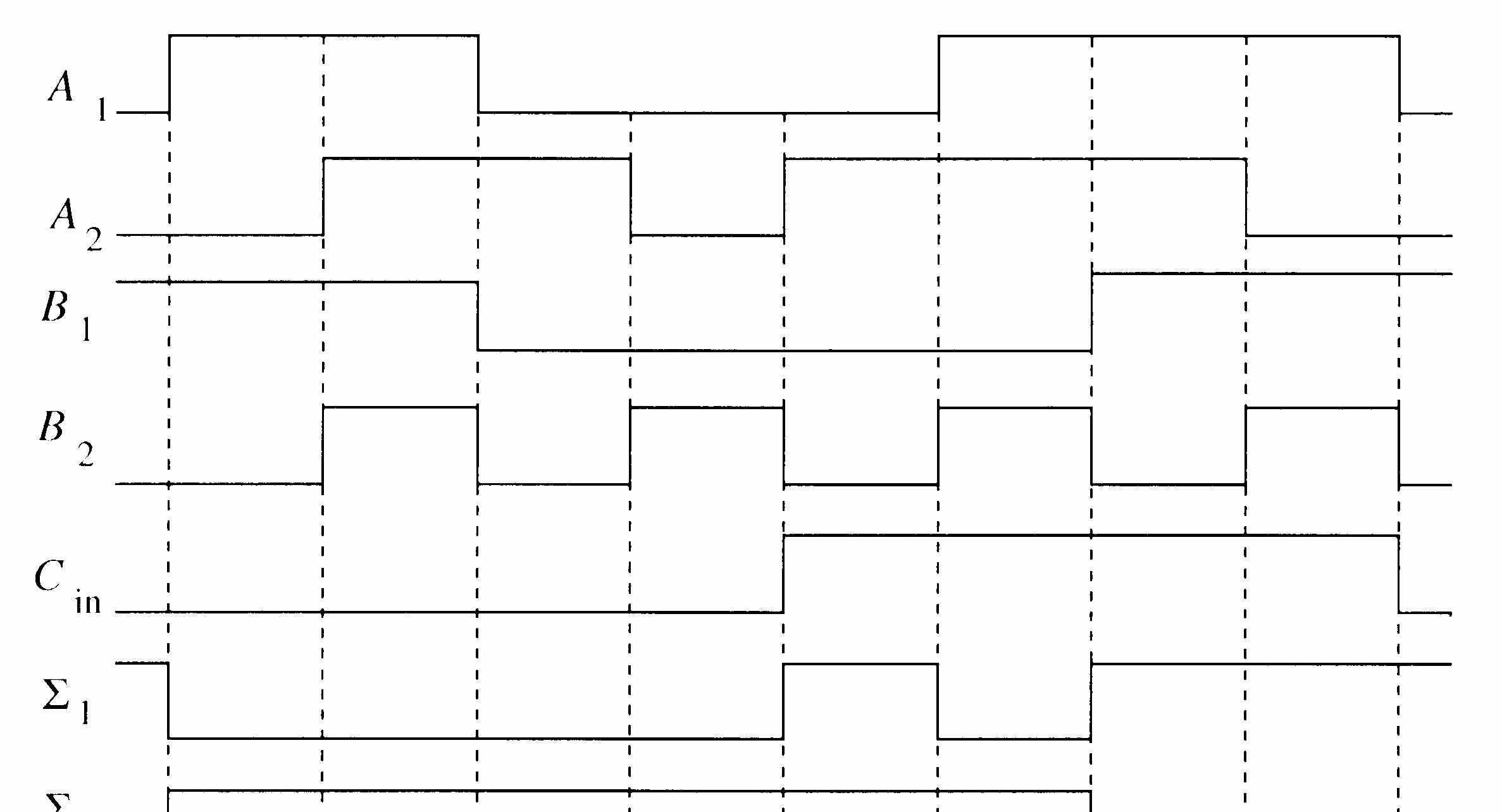
19. See Figure 1-6.
20. T = kHz 10 1 = 100 μs
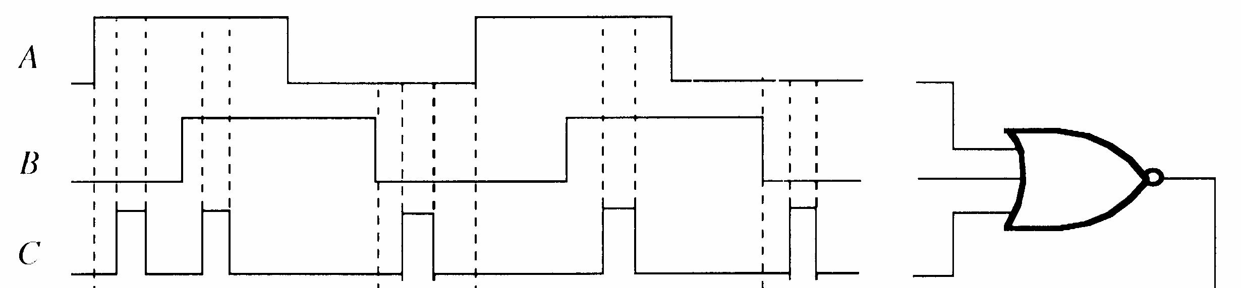
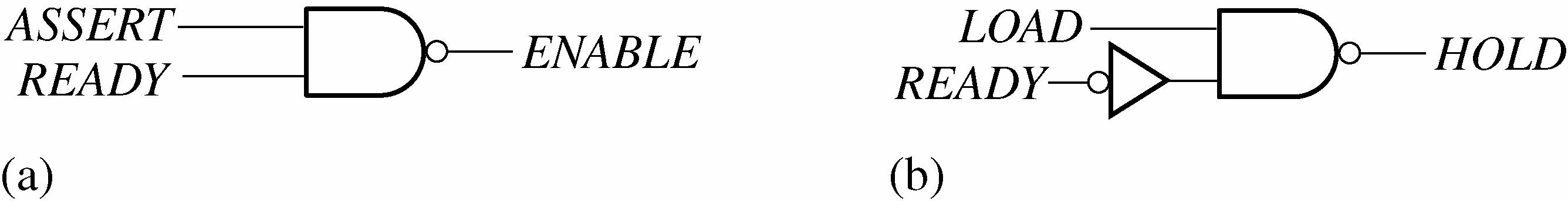
Pulses counted = s 100 ms 100 μ = 1000
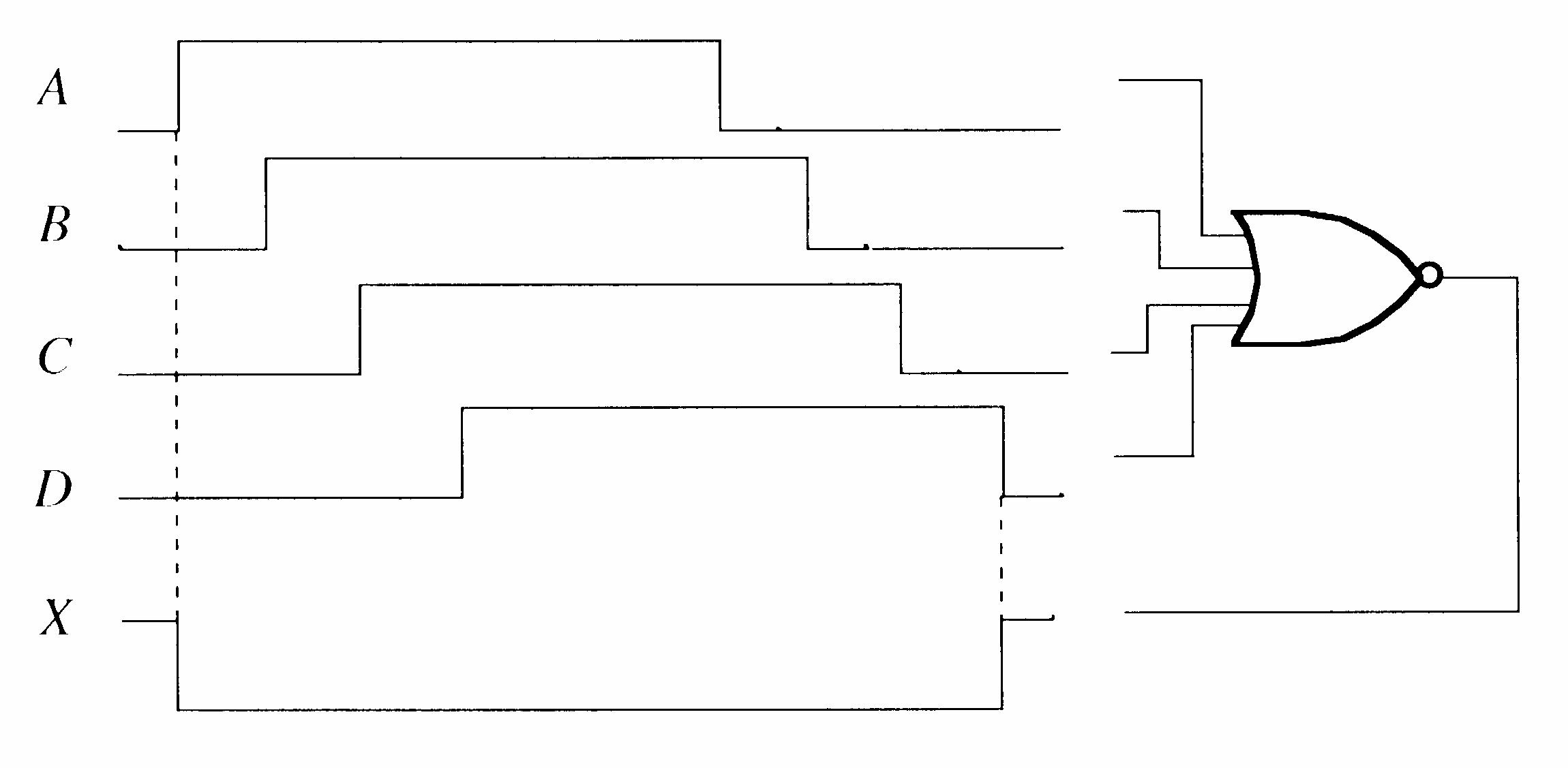
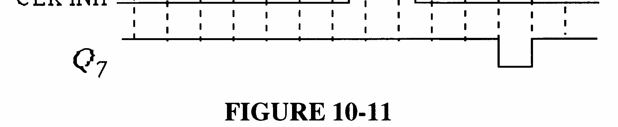
21. See Figure 1-7.
22. Circuits with complexities of from 100 to 10,000 equivalent gates are classified as large scale integration (LSI).
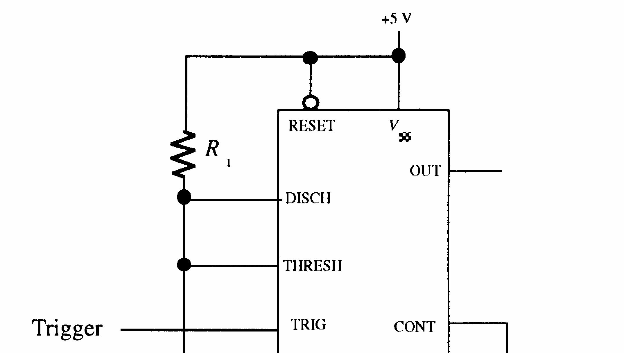
23. The pins of an SMT are soldered to the pads on the surface of a pc board, whereas the pins of a DIP feed through and are soldered to the opposite side. Pin spacing on SMTs is less than on DIPs and therefore SMT packages are physically smaller and require less surface area on a pc board.
24. See Figure 1-8.
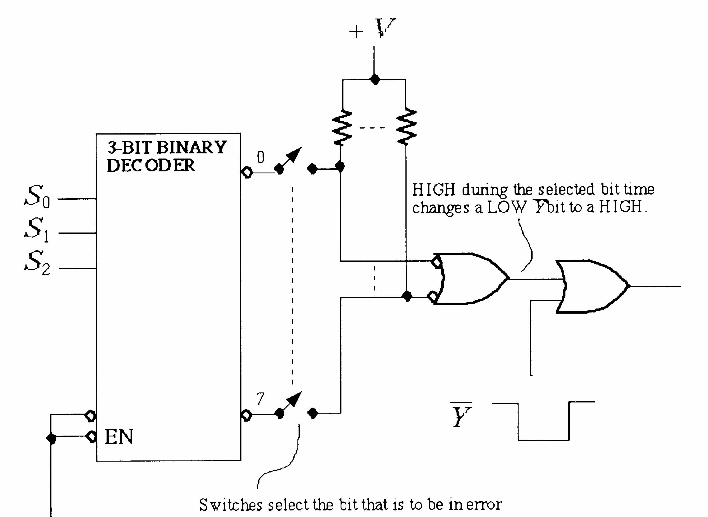
25. Amplitude = top of pulse minus base line
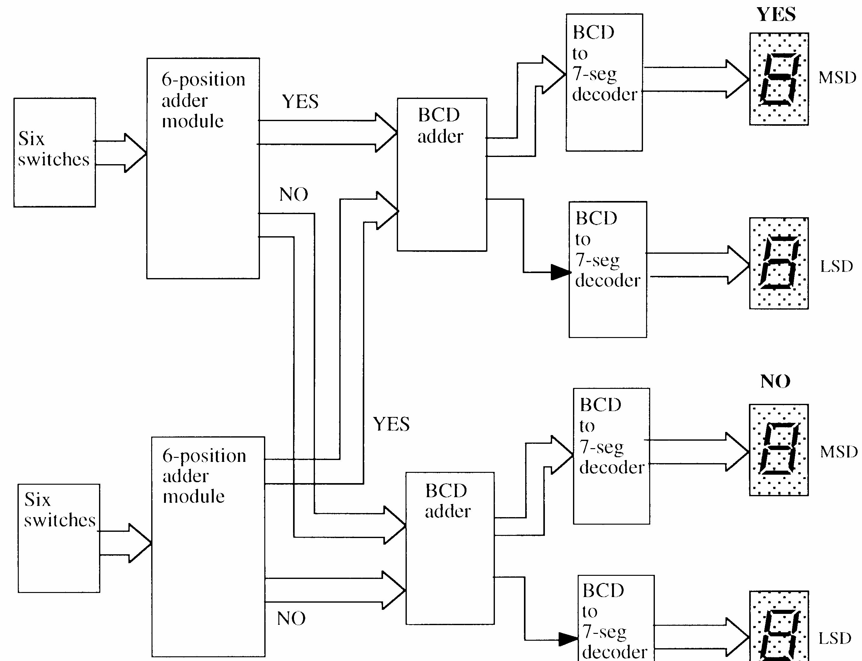
V = 8 V 1 V = 7 V
26. A flashing probe lamp indicates a continuous sequence of pulses (pulse train).
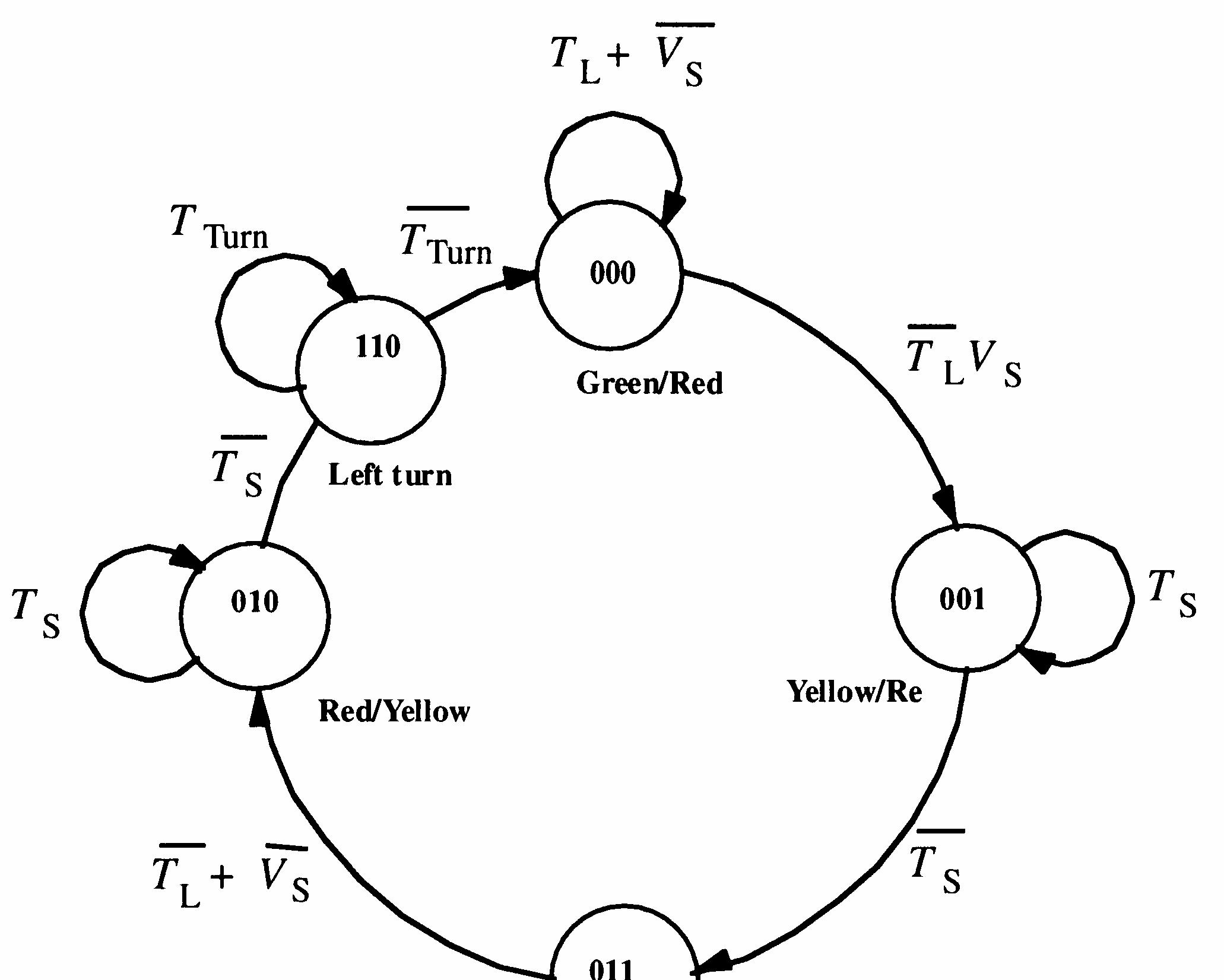
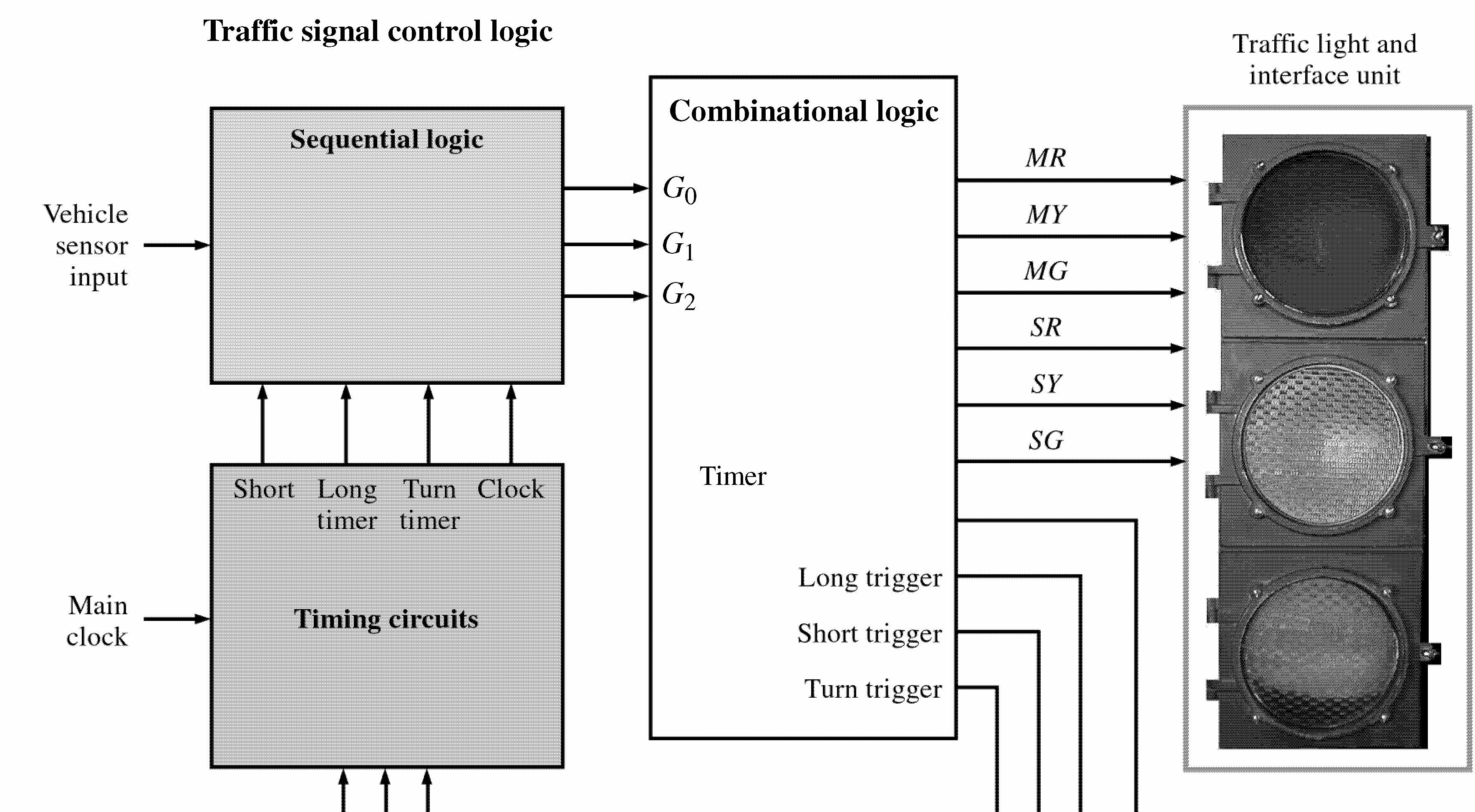
27. The following do not describe PLDs: VHDL, AHDL
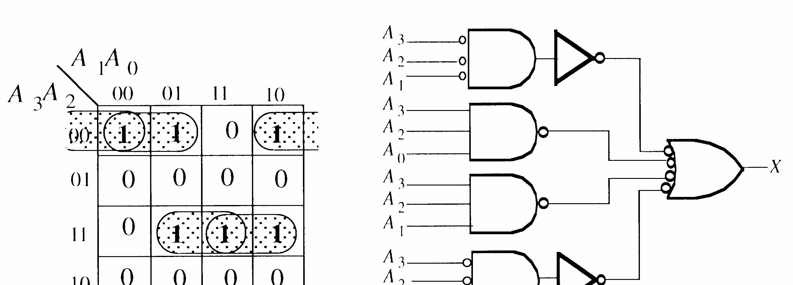
28. SPLD: Simple Programmable Logic Device
CPLD: Complex Programmable Logic Device
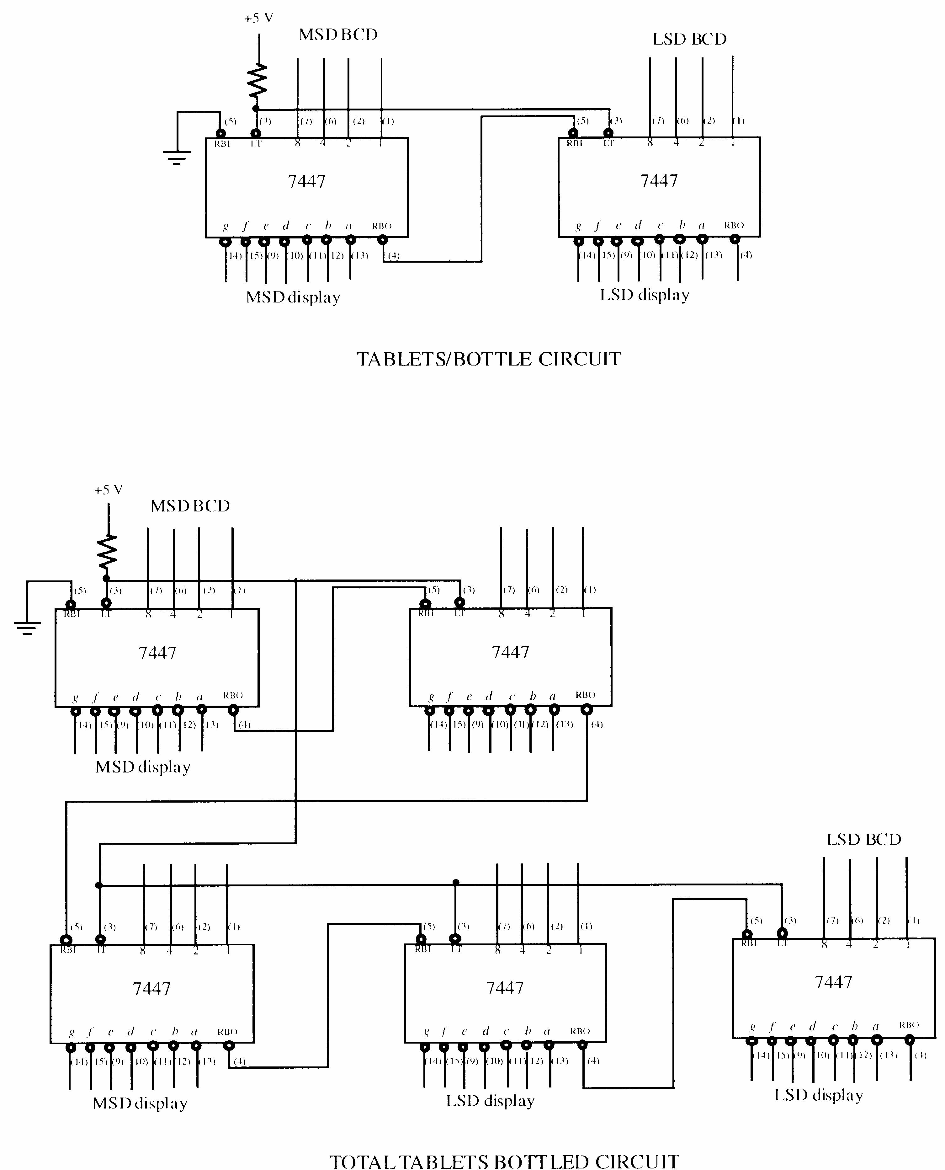
HDL: Hardware Description Language
FPGA: Field-Programmable Gate Array
GAL: Generic Array Logic
29. (a) Design entry: The step in a programmable logic design flow where a description of the circuit is entered in either schematic (graphic) form or in text form using an HDL.
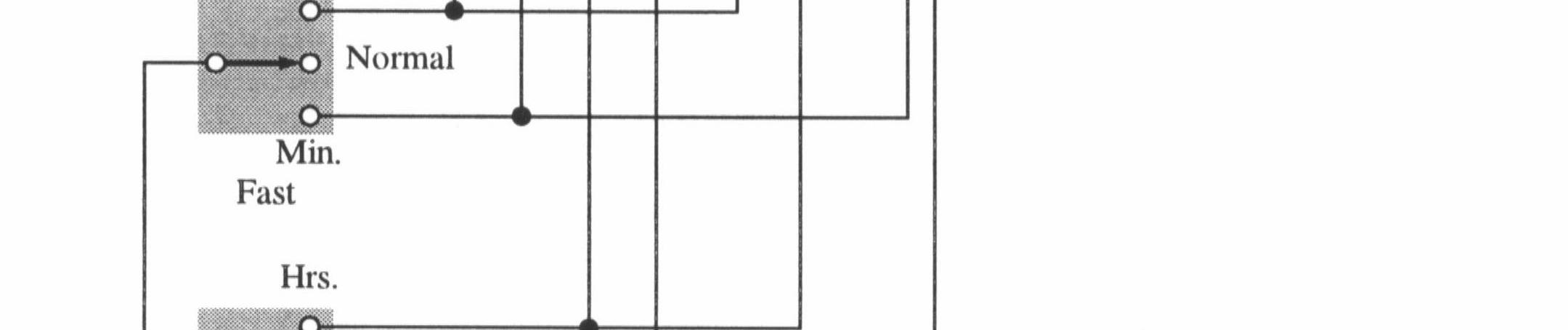
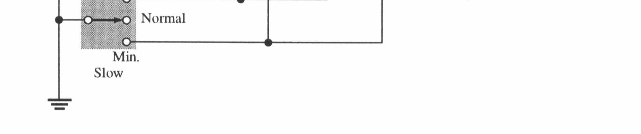
(b) Simulation: The step in a design flow where the entered design is simulated based on defined input waveforms.
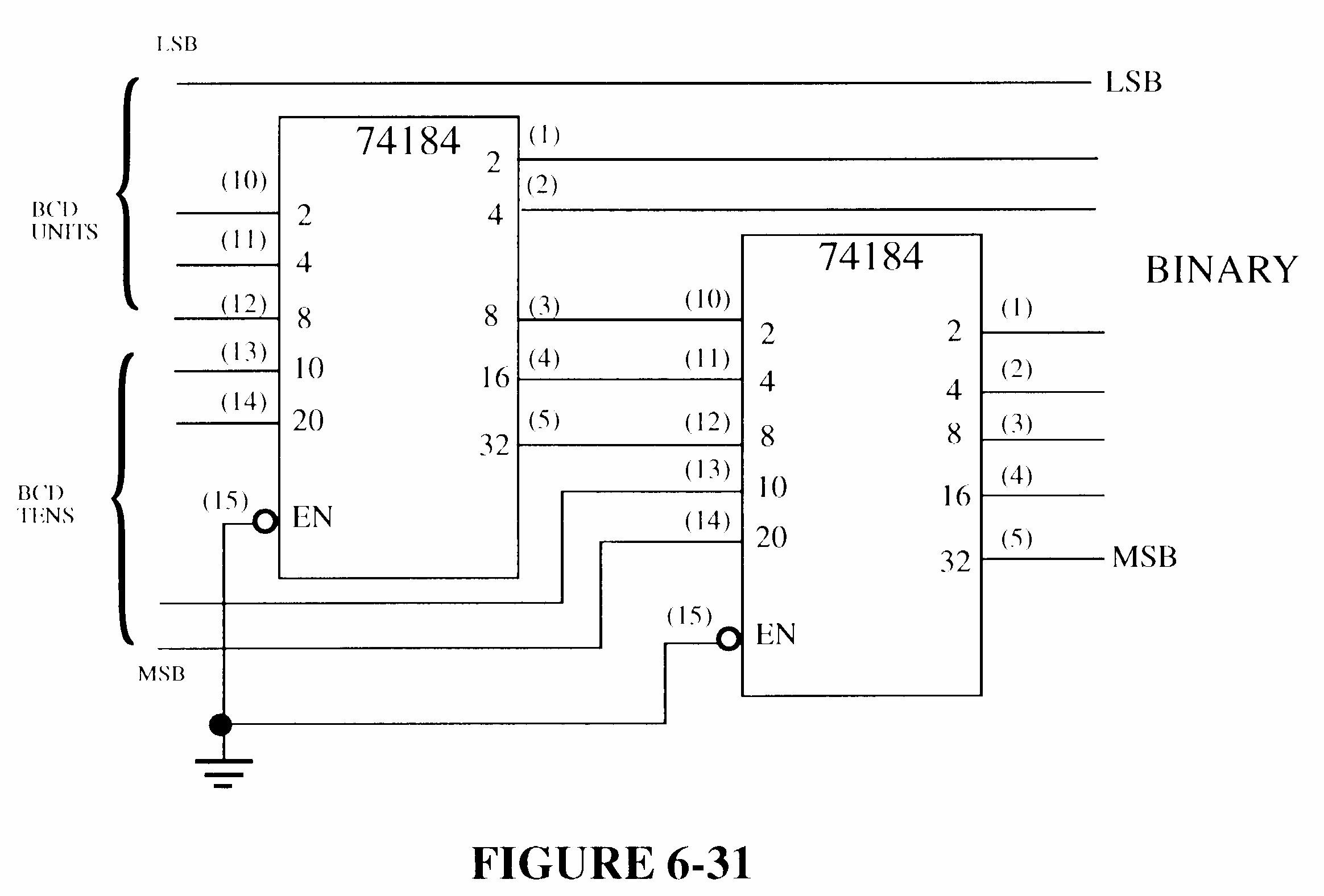
(c) Compilation: A program process that controls the design flow process and translates a design source code to object code for testing and downloading.
(d) Download: The process in which the design is transferred from software to hardware.
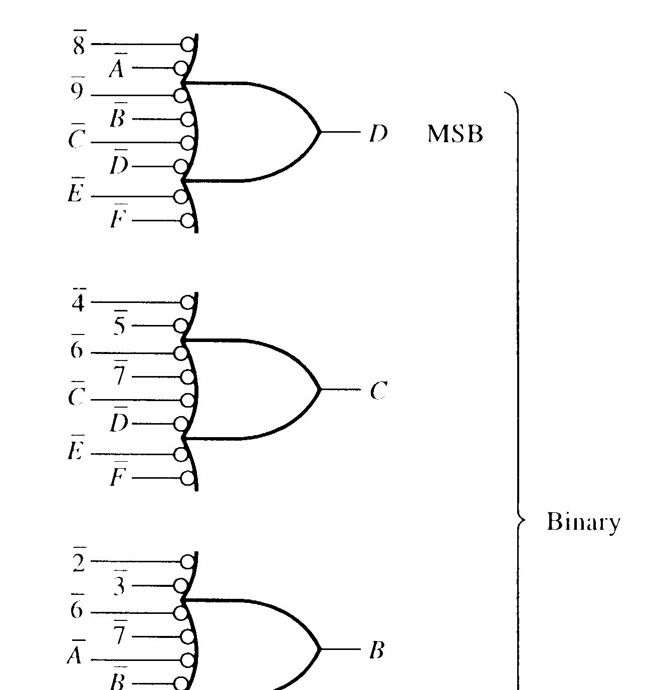
30. Place and route or fitting is the process where the logic structures described by the netlist are mapped into the actual structure of the specific target device. This results in an output called a bitstream.
Section 2-1 Decimal Numbers
1. (a) 1386 = 1 × 10³ + 3 × 10² + 8 × 101 + 6 × 100 = 1 × 1000 + 3 × 100 + 8 × 10 + 6 × 1
The digit 6 has a weight of 100 = 1
(b) 54,692 = 5 × 10⁴ + 4 × 10³ + 6 × 10² + 9 × 101 + 2 ×
= 5 × 10,000 + 4 × 1000 + 6 × 100 + 9 ×
The digit 6 has a weight of 102 = 100
(c) 671,920 = 6 × 10⁵ + 7 × 10⁴ + 1 × 10³ + 9 × 10² + 2 × 101 + 0 × 100 = 6 × 100,000 + 7 × 10,000 + 1 × 1000 + 9 × 100 + 2 × 10 + 0 × 1 The digit 6 has a weight of 105 = 100,000
2. (a) 10 = 101 (b) 100 = 102 (c) 10,000 = 104 (d) 1,000,000 = 106
3. (a) 471 = 4 × 10² + 7 × 101 + 1 × 100 = 4 × 100 + 7 × 10 + 1 × 1 = 400 + 70 + 1
(b) 9,356 = 9 × 10³ + 3 × 10² + 5 × 101 + 6 × 100 = 9 × 1000 + 3 × 100 + 5 × 10 + 6 × 1 = 9,000 + 300 + 50 + 6
(c) 125,000 = 1 × 10⁵ + 2 × 10⁴ + 5 × 103 = 1 × 100,000 + 2 × 10,000 + 5 × 1000 = 100,000 + 20,000 + 5,000
4. The highest four-digit decimal number is 9999.
5. (a) 11 = 1 × 21 + 1 × 20 = 2 + 1 = 3 (b) 100 = 1 × 22 + 0 × 21 + 0 × 20 = 4 (c) 111 = 1 × 22 + 1 × 21 + 1 × 20 = 4 + 2 + 1 = 7 (d) 1000 = 1 × 23 + 0 × 22 + 0 × 21 + 0 × 20 = 8 (e) 1001 = 1 × 23 + 0 × 22 + 0 × 21 + 1 × 20 = 8 + 1 = 9
(f) 1100 = 1 × 23 + 1 × 22 + 0 × 21 + 0 × 20 = 8 + 4 = 12 (g) 1011 = 1 × 23 + 0 × 22 + 1 × 21 + 1 × 20 = 8 + 2 + 1 = 11 (h) 1111 = 1 × 23 + 1 × 22 + 1 × 21 + 1 × 20 = 8 + 4 + 2 + 1 = 15
6. (a) 1110 = 1 × 23 + 1 × 22 + 1 × 21 = 8 + 4 + 2 = 14
(b) 1010 = 1 × 23 + 1 × 21 = 8 + 2 = 10
(c) 11100 = 1 × 24 + 1 × 23 + 1 × 22 = 16 + 8 + 4 = 28
(d) 10000 = 1 × 24 = 16
(e) 10101 = 1 × 24 + 1 × 22 + 1 × 20 = 16 + 4 + 1 = 21
(f) 11101 = 1 × 24 + 1 × 23 + 1 × 22 + 1 × 20 = 16 + 8 + 4 + 1 = 29 (g) 10111 = 1 × 24 + 1 × 22 + 1 × 21 + 1 × 20 = 16 + 4 + 2 + 1 = 23
(h) 11111 = 1 × 24 + 1 × 23 + 1 × 22 + 1 × 21 + 1 × 20 = 16 + 8 + 4 + 2 + 1 = 31
7. (a) 110011.11 = 1 × 25 + 1 × 24 + 1 × 21 + 1 × 20 + 1 × 2 1 + 1 × 2 2 = 32 + 16 + 2 + 1 + 0.5 + 0.25 = 51.75
(b) 101010.01 = 1 × 25 + 1 × 23 + 1 × 21 + 1 × 2 2 = 32 + 8 + 2 + 0.25 = 42.25
(c) 1000001.111 = 1 × 26 + 1 × 20 + 1 × 2 1 + 1 × 2 2 + 1 × 2 3 = 64 + 1 + 0.5 + 0.25 + 0.125 = 65.875
(d) 1111000.101 = 1 × 26 + 1 × 25 + 1 × 24 + 1 × 23 + 1 × 2 1 + 1 × 2 3 = 64 + 32 + 16 + 8 + 0.5 + 0.125 = 120.625 (e) 1011100.10101 = 1 × 26 + 1 × 24 + 1 × 23 + 1 × 22 + 1 × 2 1 +
×
3 +
× 2 5 = 64 + 16 + 8 + 4 + 0.5 + 0.125 + 0.03125 = 92.65625 (f) 1110001.0001 = 1 × 26 + 1 × 25 + 1 × 24 + 1 × 20 + 1 × 2 4 = 64 + 32 + 16 + 1 + 0.0625 = 113.0625 (g) 1011010.1010 = 1 × 26 + 1 × 24 + 1 × 23 + 1 ×
=
= 64 + 32 + 16 + 8 + 4 + 2 + 1 + 0.5 + 0.25 + 0.125 + 0.0625 + 0.03125 = 127.96875
8. (a) 22 1 = 3 (b) 23 1 = 7
(c) 24 1 = 15 (d) 25 1 = 31
(e) 26 1 = 63 (f) 27 1 = 127
(g) 28 1 = 255 (h) 29 1 = 511
(i) 210 1 = 1023 (j) 211 1 = 2047
9. (a) (24 1) < 17 < (25 1); 5 bits
(b) (25 1) < 35 < (26 1); 6 bits
(c) (25 1) < 49 < (26 1); 6 bits
(d) (26 1) < 68 < (27 1); 7 bits
(e) (26 1) < 81 < (27 1); 7 bits
(f) (26 1) < 114 < (27 1); 7 bits
(g) (27 1) < 132 < (28 1); 8 bits
(h) (27 1) < 205 < (28 1); 8 bits
10. (a) 0 through 7:
000, 001, 010, 011, 100, 101, 110, 111
(b) 8 through 15:
1000, 1001, 1010, 1011, 1100, 1101, 1110, 1111
(c) 16 through 31:
10000, 10001, 10010, 10011, 10100, 10101, 10110, 10111, 11000, 11001, 11010, 11011, 11100, 11101, 11110, 11111
(d) 32 through 63:
100000, 100001, 100010, 100011, 100100, 100101, 100110, 100111, 10100, 101001, 101010, 101011, 101100, 101101, 101110, 101111, 110000, 110001, 110010, 110011, 110100, 110101, 110110, 110111, 111000, 111001, 111010, 111011, 111100, 111101, 111110, 111111
(e) 64 through 75:
1000000, 1000001, 1000010, 1000011, 1000100, 1000101, 1000110, 1000111, 1001000, 1001001, 1001010, 1001011
11. (a) 10 = 8 + 2 = 23 + 21 = 1010
(b) 17 = 16 + 1 = 24 + 20 = 10001
(c) 24 = 16 + 8 = 24 + 23 = 11000
(d) 48 = 32 + 16 = 25 + 24 = 110000
(e) 61 = 32 + 16 + 8 + 4 + 1 = 25 + 24 + 23 + 22 + 20 = 111101
(f) 93 = 64 + 16 + 8 + 4 + 1 = 26 + 24 + 23 + 22 + 20 = 1011101
(g) 125 = 64 + 32 + 16 + 8 + 4 + 1 = 26 + 25 + 24 + 23 + 22 + 20 = 1111101
(h) 186 = 128 + 32 + 16 + 8 + 2 = 27 + 25 + 24 + 23 + 21 = 10111010
12. (a) 0.32 ≅ 0.00 + 0.25 + 0.0625 + 0.0 + 0.0 + 0.0078125 = 0.0101001
(b) 0.246 ≅ 0.0 + 0.0 + 0.125 + 0.0625 + 0.03125 + 0.015625 = 0.001111
(c) 0.0981 ≅ 0.0 + 0.0 + 0.0 + 0.0625 + 0.03125 + 0.0 + 0.0 + 0.00390625 = 0.0001101
13. (a) 2 15 = 7, R = 1( LSB) 2 7 = 3, R = 1 2 3 = 1, R = 1 2 1 = 0, R = 1 (MSB)
(d) 2 34 = 17, R = 0 (LSB) 2 17 = 8, R = 1 2 8 = 4, R = 0 2 4 = 2, R = 0 2 2 = 1, R = 0 2 1 = 0, R = 1 (MSB)
(g) 2 65 = 32, R = 1 (LSB) 2 32 = 16, R = 0 2 16 = 8, R = 0 2 8 = 4, R = 0 2 4 = 2, R = 0 2 2 = 1, R = 0 2 1 = 0, R = 1(MSB) (b) 2 21 = 10, R = 1 (LSB) 2 10 = 5, R = 0 2 5 = 2, R = 1 2 2 = 1, R = 0 2 1 = 0, R = 1 (MSB) (e) 2 40 = 20, R = 0 (LSB) 2 20 = 10, R = 0 2 10 = 5, R = 0
2 = 1, R = 0 2 1 = 0, R = 1 (MSB) (h) 2 73 = 36, R = 1 (LSB) 2 36 = 18, R = 0 2 18 = 9, R = 0 2 9 = 4, R = 1 2 4 = 2, R = 0 2 2 = 1, R = 0 2 1 = 0, R = 1 (MSB) (c) 2 28 = 14, R = 0 (LSB) 2 14 = 7, R = 0 2 7 = 3, R = 1 2 3 = 1, R = 1 2 1 = 0, R = 1 (MSB) (f) 2 59 = 29, R = 1 (LSB) 2 29 = 14, R = 1 2 14 = 7, R = 0 2 7 = 3, R = 1 2 3 = 1, R = 1 2 1 = 0, R = 1 (MSB)
5 = 2, R = 1
14. (a)
0.98 × 2 = 1.96 1 (MSB) (b) 0.347 × 2 = 0.694 0 (MSB)
0.96 × 2 = 1.92 1
0.92 × 2 = 1.84 1
0.84 × 2 = 1.68 1
0.68 × 2 = 1.36 1
0.36 × 2 = 0.72 0
continue if more accuracy is desired
0.111110
(c) 0.9028 × 2 = 1.8056 1 (MSB)
0.8056 × 2 = 1.6112 1
0.6112 × 2 = 1.2224 1
0.2224 × 2 = 0.4448 0
0.4448 × 2 = 0.8896 0
0.8896 × 2 = 1.7792 1
0.7792 × 2 = 1.5584 1
continue if more accuracy is desired
0.1110011
0.694 × 2 = 1.388 1
0.388 × 2 = 0.776 0
0.776 × 2 = 1.552 1
0.552 × 2 = 1.104 1
0.104 × 2 = 0.208 0
0.208 × 2 = 0.416 0
continue if more accuracy is desired
0.0101100
19. Zero is represented in 1’s complement as all 0’s (for +0) or all 1’s (for 0).
20. Zero is represented by all 0’s only in 2’s complement.
21. (a) The 1’s complement of 101 is 010.
(b) The 1’s complement of 110 is 001.
(c) The 1’s complement of 1010 is 0101.
(d) The 1’s complement of 11010111 is 00101000.
(e) The 1’s complement of 1110101 is 0001010.
(f) The 1’s complement of 00001 is 11110.
22. Take the 1’s complement and add 1:
(a) 01 + 1 = 10 (b) 000 + 1 = 001
(c) 0110 + 1 = 0111 (d) 0010 + 1 = 0011
(e) 00011 + 1 = 00100 (f) 01100 + 1 = 01101
(g) 01001111 + 1 = 01010000 (h) 11000010 + 1 = 11000011
23. (a) Magnitude of 29 = 0011101
(b) Magnitude of 85 = 1010101 + 29 = 00011101 85 = 11010101
(c) Magnitude of 10010 = 1100100
(d) Magnitude of 123 = 1111011 +100 = 01100100 123 = 11111011
24. (a) Magnitude of 34 = 0100010
(b) Magnitude of 57 = 0111001 34 = 11011101 +57 = 00111001
(c) Magnitude of 99 = 1100011
(d) Magnitude of 115 = 1110011 99 = 10011100 +115 = 01110011
25. (a) Magnitude of 12 = 1100
(b) Magnitude of 68 = 1000100 +12 = 00001100 68 = 10111100
(c) Magnitude of 10110 = 1100101
(d) Magnitude of 125 = 1111101 +10110 = 01100101 125 = 10000011
26. (a) 10011001 = 25 (b) 01110100 = +116 (c) 10111111 = 63
27. (a) 10011001 = (01100110) = 102 (b) 01110100 = +(1110100) = +116 (c) 10111111 = (1000000) = 64
28. (a) 10011001 = (1100111) = 103 (b) 01110100 = +(1110100) = +116 (c) 10111111 = (1000001) = 65
29. (a) 0111110000101011 → sign = 0
1.11110000101011 × 214 → exponent = 127 + 14 + 141 = 10001101
Mantissa = 11110000101011000000000 01000110111110000101011000000000
(b) 100110000011000 → sign = 1
1.10000011000 × 211 → exponent = 127 + 11 = 138 = 10001010
Mantissa = 11000001100000000000000 11000101011000001100000000000000
30. (a) 11000000101001001110001000000000
Sign = 1
Exponent = 10000001 = 129 127 = 2
Mantissa = 1.01001001110001 × 22 = 101.001001110001 101.001001110001 = 5.15258789
(b) 01100110010000111110100100000000
Sign = 0
Exponent = 11001100 = 204 127 = 77
Mantissa = 1.100001111101001 1.100001111101001 × 277
31. (a) 33 = 00100001 00100001 15 = 00001111 + 00001111 00110000
(c) 46 = 00101110 11010010
46 = 11010010 + 00011001 25 = 00011001 11101011
32. (a) 00010110 (b) 01110000 + 00110011 + 10101111 01001001 100011111
33. (a) 10001100 (b) 11011001 + 00111001 + 11100111 11000101 11000000
(b) 56 = 00111000 00111000
27 = 00011011 + 11100101
27 = 11100101 00011101
(d) 11010 = 01101110 10010010
11010 = 10010010 + 10101100 84 = 01010100 100111110 84 = 10101100
34. (a) 00110011 00110011 00010000 + 11110000 1 00100011 (b) 01100101 01100101 11101000 + 00011000 01111101
35. 01101010 01101010 × 11110001 × 00001111 01101010 01101010 100111110 01101010 1011100110 01101010 11000110110
Changing to 2’s complement with sign: 100111001010
36. 00011001 01000100 = 00000010
25 68 = 2, remainder of 18
37. (a) 3816 = 0011 1000
(b) 5916 = 0101 1001
(c) A1416 = 1010 0001 0100
(d) 5C816 = 0101 1100 1000
(e) 410016 = 0100 0001 0000 0000
(f) FB1716 = 1111 1011 0001 0111
(g) 8A9D16 = 1000 1010 1001 1101
38. (a) 1110 = E16
(b) 10 = 216
(c) 0001 0111 = 1716
(d) 1010 0110 = A616
(e) 0011 1111 0000 = 3F016
(f) 1001 1000 0010 = 98216
39. (a) 2316 = 2 × 161 + 3 × 160 = 32 + 3 = 35
(b) 9216 = 9 × 161 + 2 × 160 = 144 + 2 = 146
(c) 1A16 = 1 × 161 + 10 × 160 = 16 + 10 = 26
(d) 8D16 = 8 × 161 + 13 × 160 = 128 + 13 = 141
(e) F316 = 15 × 161 + 3 × 160 = 240 + 3 = 243
(f) EB16 = 14 × 161 + 11 × 160 = 224 + 11 = 235
(g) 5C216 = 5 × 162 + 12 × 161 + 2 × 160 = 1280 + 192 + 2 = 1474
(h) 70016 = 7 × 162 = 1792
40. (a) 16 8 = 0, remainder = 8
hexadecimal number = 816
(c) 16 33 = 2, remainder = 1 (LSD)
16 2 = 0, remainder = 2
hexadecimal number = 2116
(e) 16 284 = 17, remainder = 12 = C16 (LSD) 16 17 = 1, remainder = 1 16 1 = 0, remainder = 1
hexadecimal number = 11C16
(g) 16 4019 = 251, remainder = 3 (LSD) 16 251 = 15, remainder = 11 = B16 16 15 = 0, remainder = 15 = F16
hexadecimal number = E16
hexadecimal number = FB316 (b) 16 14 = 0, remainder = 14 = E16
41. (a) 3716 + 2916 = 6016
(b) A016 + 6B16 = 10B16 (c) FF16 + BB16 = 1BA16
(d) 16 52 = 3, remainder = 4 (LSD) 16 3 = 0, remainder = 3
hexadecimal number = 3416 (f) 16 2890 = 180, remainder = 10 = A16 (LSD) 16 180 = 11, remainder = 4 0 16 11 = , remainder = 11 = B16
hexadecimal number = B4A16 (h) 16 6500 = 406, remainder = 4 (LSD) 16 406 = 25, remainder = 6 16 25 = 1, remainder = 9 16 1 = 0, remainder = 1
hexadecimal number = 196416
42. (a) 5116 4016 = 1116
(b) C816 3A16 = 8E16
(c) FD16 8816 = 7516
43. (a) 128 = 1 × 81 + 2 × 80 = 8 + 2 = 10
(b) 278 = 2 × 81 + 7 × 80 = 16 + 7 = 23
(c) 568 = 5 × 81 + 6 × 80 = 40 + 6 = 46
(d) 648 = 6 × 81 + 4 × 80 = 48 + 4 = 52
(e) 1038 = 1 × 82 + 3 × 80 = 64 + 3 = 67
(f) 5578 = 5 × 82 + 5 × 81 + 7 × 80 = 320 + 40 + 7 = 367
(g) 1638 = 1 × 82 + 6 × 81 + 3 × 80 = 64 + 48 + 3 = 115
(h) 10248 = 1 × 83 + 2 × 81 + 4 × 80 = 512 + 16 + 4 = 532
(i) 77658 = 7 × 83 + 7 × 82 + 6 × 81 + 5 × 80 = 3584 + 448 + 48 + 5 = 4085
44. (a) 8 15 = 1, remainder = 7 (LSD)
8 1 = 0, remainder =1
octal number = 178
(c) 8 46 = 5, remainder = 6 (LSD)
8 5 = 0, remainder = 5
octal number = 568
(e) 8 100 = 12, remainder = 4 (LSD)
8 12 = 1, remainder = 4
8 1 = 0, remainder = 1
octal number = 1448
(g) 8 219 = 27, remainder = 3 (LSD)
8 27 = 3, remainder = 3
8 3 = 0, remainder = 3
octal number = 3338
(b) 8 27 = 3, remainder = 3 (LSD) 8 3 = 0, remainder = 3
octal number = 338
(d) 8 70 = 8, remainder = 6 (LSD)
8 8 = 1, remainder = 0
8 1 = 0, remainder = 1
octal number = 1068
(f) 8 142 = 17, remainder = 6 (LSD) 8 17 = 2, remainder = 1 8 2 = 0, remainder = 2
octal number = 2168
(h) 8 435 = 54, remainder = 3 (LSD)
8 54 = 6, remainder = 6
8 6 = 0, remainder = 6
octal number = 6638
45. (a) 138 = 001 011
(b) 578 = 101 111
(c) 1018 = 001 000 001
(d) 3218 = 011 010 001
(e) 5408 = 101 100 000
(f) 46538 = 100 110 101 011
(g) 132718 = 001 011 010 111 001
(h) 456008 = 100 101 110 000 000
(i) 1002138 = 001 000 000 010 001 011
46. (a) 111 = 78
(b) 010 = 28
(c) 110 111 = 678
(d) 101 010 = 528
(e) 001 100 = 148
(f) 001 011 110 = 1368
(g) 101 100 011 001 = 54318
(h) 010 110 000 011 = 26038
(i) 111 111 101 111 000 = 775708
47. (a) 10 = 0001 0000
(b) 13 = 0001 0011
(c) 18 = 0001 1000
(d) 21 = 0010 0001
(e) 25 = 0010 0101
(f) 36 = 0011 0110
(g) 44 = 0100 0100
(h) 57 = 0101 0111
(i) 69 = 0110 1001
(j) 98 = 1001 1000
(k) 125 = 0001 0010 0101
(l) 156 = 0001 0101 0110
48. (a) 10 = 10102 4 bits binary, 8 bits BCD
(b) 13 = 11012 4 bits binary, 8 bits BCD
(c) 18 = 100102 5 bits binary, 8 bits BCD
(d) 21 = 101012 5 bits binary, 8 bits BCD
(e) 25 = 110012 5 bits binary, 8 bits BCD
(f) 36 = 1001002 6 bits binary, 8 bits BCD
(g) 44 = 1011002 6 bits binary, 8 bits BCD
(h) 57 = 1110012 6 bits binary, 8 bits BCD
(i) 69 = 10001012 7 bits binary, 8 bits BCD
(j) 98 = 11000102 7 bits binary, 8 bits BCD
(k) 125 = 11111012 7 bits binary, 12 ibts BCD
(l) 156 = 100111002 8 bits binary, 12 bits BCD
49. (a) 104 = 0001 0000 0100
(b) 128 = 0001 0010 1000
(c) 132 = 0001 0011 0010
(d) 150 = 0001 0101 0000
(e) 186 = 0001 1000 0110
(f) 210 = 0010 0001 0000
(g) 359 = 0011 0101 1001
(h) 547 = 0101 0100 0111
(i) 1051 = 0001 0000 0101 0001
50. (a) 0001 = 1 (b) 0110 = 6
(c) 1001 = 9 (d) 0001 1000 = 18
(e) 0001 1001 = 19 (f) 0011 0010 = 32
(g) 0100 0101 = 45 (h) 1001 1000 = 98
(i) 1000 0111 0000 = 870
51. (a) 1000 0000 = 80
(b) 0010 0011 0111 = 237
(c) 0011 0100 0110 = 346
(d) 0100 0010 0001 = 421
(e) 0111 0101 0100 = 754
(f) 1000 0000 0000 = 800
(g) 1001 0111 1000 = 978
(h) 0001 0110 1000 0011 = 1683
(i) 1001 0000 0001 1000 = 9018
(j) 0110 0110 0110 0111 = 6667
52. (a) 0010 + 0001 0011
(d) 1000 + 0001 1001
(g) 01000000 + 01000111 10000111
(b) 0101 + 0011 1000
(e) 00011000 + 00010001 00101001
(h) 10000101 + 00010011 10000111
(c) 0111 + 0010 1001
(f) 01100100 + 00110011 10010111
53. (a)
00010100 0110 1110 0110 1000 + +
(c)
00010111 0110 10001 1000 1001 + + (e)
01010010 0110 01001100 00100111 00100101 + + (g)
000110010101 01100110 100101111 10010111 10011000 + +
00010010 0110 1100 0101 0111 + + (d)
00010110 0110 10000 0111 1001 + + (f)
000100001001 0110 10101001 01011000 01010001 + + (h)
0001001001101001 0110 110001101001 011100001000 010101100001 + +
54. (a) 4 + 3
0111 0011 0100 +
(c) 6 + 4
00010000 0110 1010 0100 0110 + +
(e) 28 + 23
01010001 0110 01001011 00100011 00101000 + +
(b) 5 + 2 0111 0010 0101 + (d) 17 + 12 00101001 00100010 00010111 + (f) 65 + 58
000100100011 01100110 10111101 01011000 01100101 + +
(g) 113 + 101 001000010100
000100000001 000100010011 +
(h) 295 + 157 010001010010 01100110 001111101100 000101010111 001010010101 + +
55. The Gray code makes only one bit change at a time when going from one number in the sequence to the next number. Gray for 11112 = 1000 Gray for 00002 = 0000
56. (a)
57. (a) 1 0 1 0 Gray (b) 0 0 0 1 0 Gray 1 1 0 0 Binary 0
58. (a) 1 → 00110001 (b) 3 → 00110011 (c) 6 → 00110110 (d) 10 → 0011000100110000
(e) 18 → 0011000100111000 (f) 29 → 0011001000111001 (g) 56 → 0011010100110110 (h) 75 → 0011011100110101 (i) 107 → 001100010011000000110111
59. (a) 0011000 → CAN (b) 1001010 → J (c) 0111101 → = (d) 0100011 → # (e) 0111110 → > (f) 1000010 → B
60. 1001000 1100101 1101100 1101100 1101111 0101110 0100000 H e l l o . # 1001000 1101111 1110111 0100000 1100001 1110010 1100101
61. 1001000 1100101 1101100 1101100 1101111 0101110 0100000
48 65 6C 6C 6F 2E 20 1001000 1101111 1110111 0100000 1100001 1110010 1100101
48 6F 77 20 61 72 65 0100000 1111001 1101111 1110101 0111111 20 79 6F 75 3F
62. 30 INPUT A, B
3 0110011 3316
0 0110000 3016
SP 0100000 2016
I 1001001 4916
N 1001110 4E16
P 1010000 5016
U 1010101 5516
T 1010100 5416
SP 0100000 2016
A 1000001 4116
, 0101100 2C16
B 1000010 4216
Section 2-12 Error Detection Codes
63. Code (b) 011101010 has five 1s, so it is in error.
64. Codes (a) 11110110 and (c) 01010101010101010 are in error because they have an even number of 1s.
65. (a) 1 10100100 (b) 0 00001001 (c) 1 11111110
66. (a)
67. (a)
In each case, you get the other number.
68. 101100100000
Remainder0110 =
Append remainder to data.
69. Error in MSB of transmitted CRC:
CRC is 101100100110.
Remainder is 10, indicating an error.
Section 3-1 The Inverter
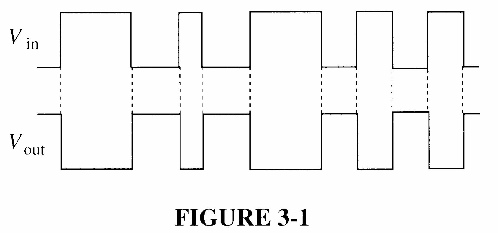
1. See Figure 3-1.
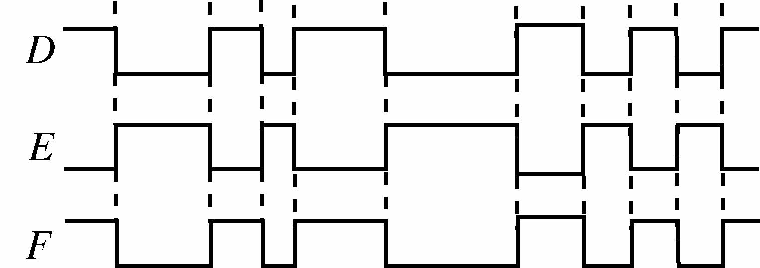
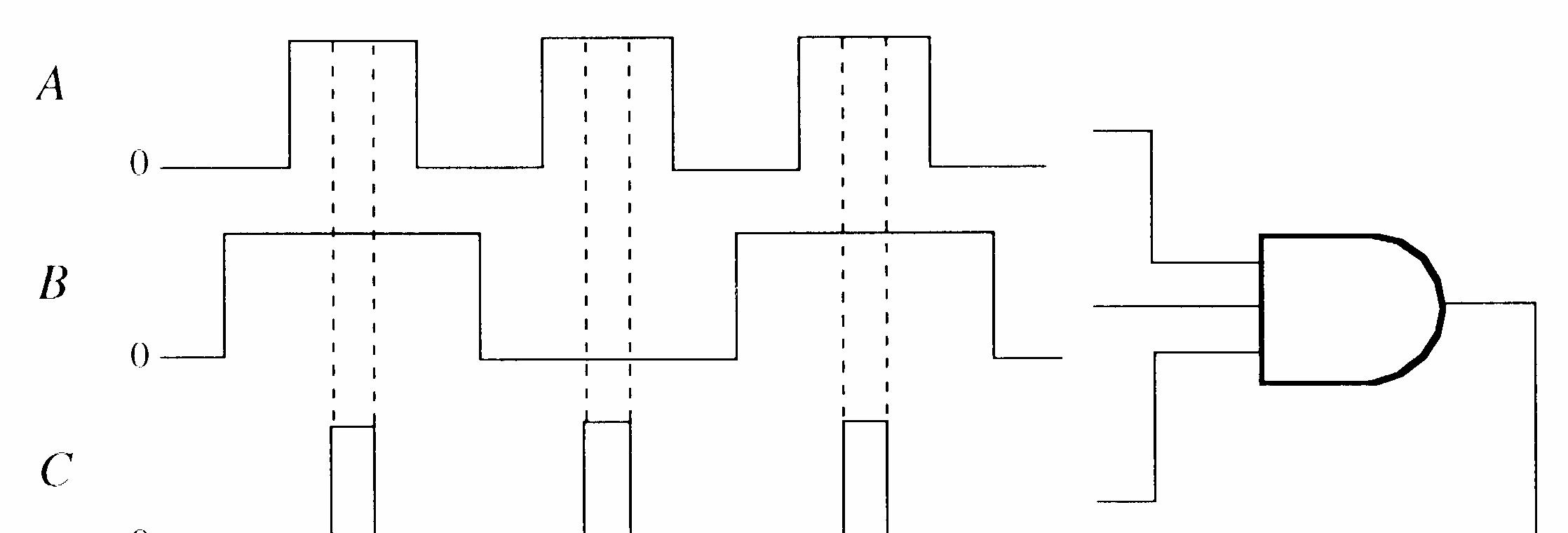
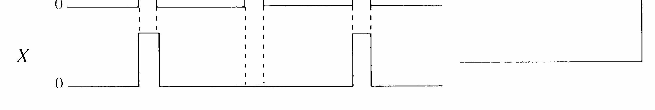
2. B: LOW, C: HIGH, D: LOW, E: HIGH, F: LOW
3. See Figure 3-2.
Section 3-2 The AND Gate
4. See Figure 3-3.
3-3
5. See Figure 3-4.
3-4
6. See Figure 3-5.
7. See Figure 3-6.
3-5
3-6
8. See Figure 3-7.
3-7
Section 3-3 The OR Gate
9. See Figure 3-8.
10. See Figure 3-9.
3-8
3-9
11. See Figure 3-10.
3-10
12. See Figure 3-11.
3-11
See Figure 3-12.
3-12
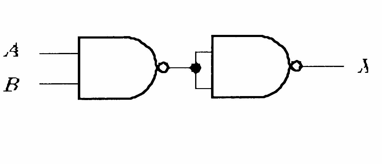
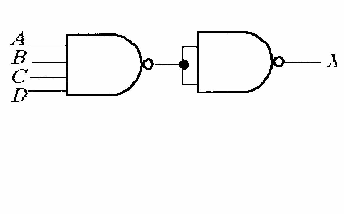
Section 3-4 The NAND Gate
15. See Figure 3-13.
16. See Figure 3-14.
FIGURE 3-13
FIGURE 3-14
17. See Figure 3-15.
FIGURE 3-15
18. See Figure 3-16.
3-16
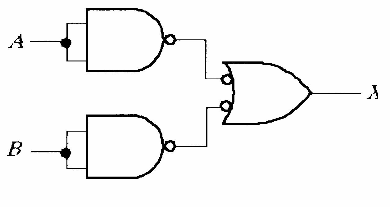
Section 3-5 The NOR Gate
19. See Figure 3-17.
20. See Figure 3-18.
3-17
3-18
21. See Figure 3-19.
3-19
22. See Figure 3-20.
3-20
Section 3-6 The Exclusive-OR and Exclusive-NOR Gates
23. The output of the XOR gate is HIGH only when one input is HIGH. The output of the OR gate is HIGH any time one or more inputs are HIGH.
XOR = AB B A + OR = A + B
24. See Figure 3-21.
FIGURE 3-21
25. See Figure 3-22.
3-22
26. See Figure 3-23.
3-23
27. The power dissipation of CMOS increases with frequency.
28. (a) P = CCHCCL CC 1.6 mA4.4 mA 5.5 V 22
= 16.5 mW
(b) VOH(min) = 2.7 V
(c) tPLH = TPHL = 15 ns
(d) VOL = 0.4 V (max)
(e) @ VCC = 2 V, tPHL = tPLH = 75 ns; @ VCC = 6 V, tPHL = tPLH = 13 ns
29. See Figure 3-24.
3-24
30. Gate A can be operated at the highest frequency because it has shorter propagation delay times than Gate B.
31. PD = VCCIC = (5 V)(4 mA) = 20 mW
32. ICCH = 4 mA; PD = (5 V)(4 mA) = 20 mW
33. (a) NAND gate OK
(b) AND gate faulty
(c) NAND gate faulty
(d) NOR gate OK
(e) XOR gate faulty
(f) XOR gate OK
34. (a) NAND gate faulty. Input A open. (b) NOR gate faulty. Input B shorted to ground.
(c) NAND gate OK
(d) XOR gate faulty. Input A open.
35. (a) The gate does not respond to pulses on either input when the other input is HIGH. It is unlikely that both inputs are open. The most probable fault is that the output is stuck in the LOW state (shorted to ground, perhaps) although it could be open.
(b) Pin 4 input or pin 6 output internally open.
36. The timer input to the AND gate is open. Check for 30-second HIGH level on this input when ignition is turned on.
37. An open seat-belt input to the AND gate will act like a constant HIGH just as if the seat belt were unbuckled.
38. Two possibilities: An input stuck LOW or the output stuck HIGH.
39. X1 = AB
X2 = B A
X3 = B A
40. X1 = ABC
Row 1: blow
C C B B A and , , , , column fuses
Row 2: blow C C B A A and , , , , column fuses
Row 3: blow C B B A A and , , , , column fuses
X2 = ABC
Row 4: blow C C B B A and , , , ,column fuses
Row 5: blow C C B A A and , , , ,column fuses
Row 6: blow ,,,, and AABBC column fuses
X3 = ABC
Row 7: blow
Row 8: blow
C C B B A and , , , ,column fuses
C C B A A and , , , ,column fuses
Row 9: blow C B B A A and , , , ,column fuses
41. See Figure 3-25.
FIGURE 3-25
42. See Figure 3-26.

FIGURE 3-26
43. Add an inverter to the Enable input line of the AND gate as shown in Figure 3-27.
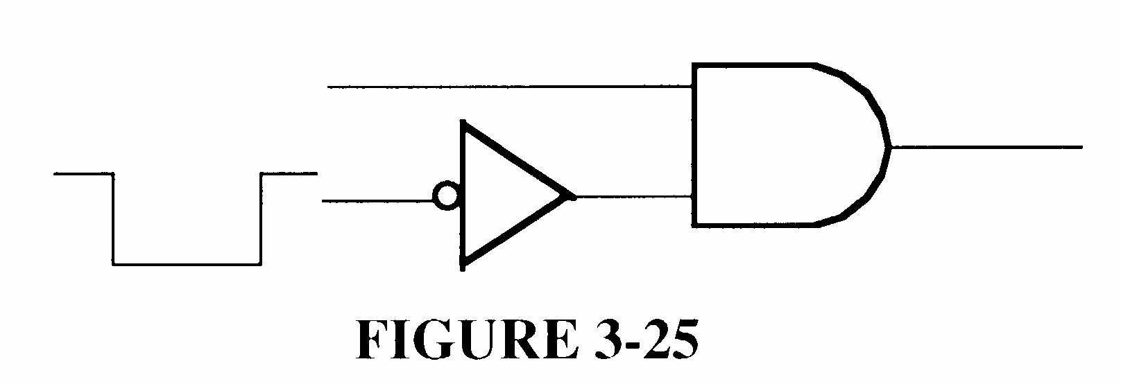
FIGURE 3-27
44. See Figure 3-28.
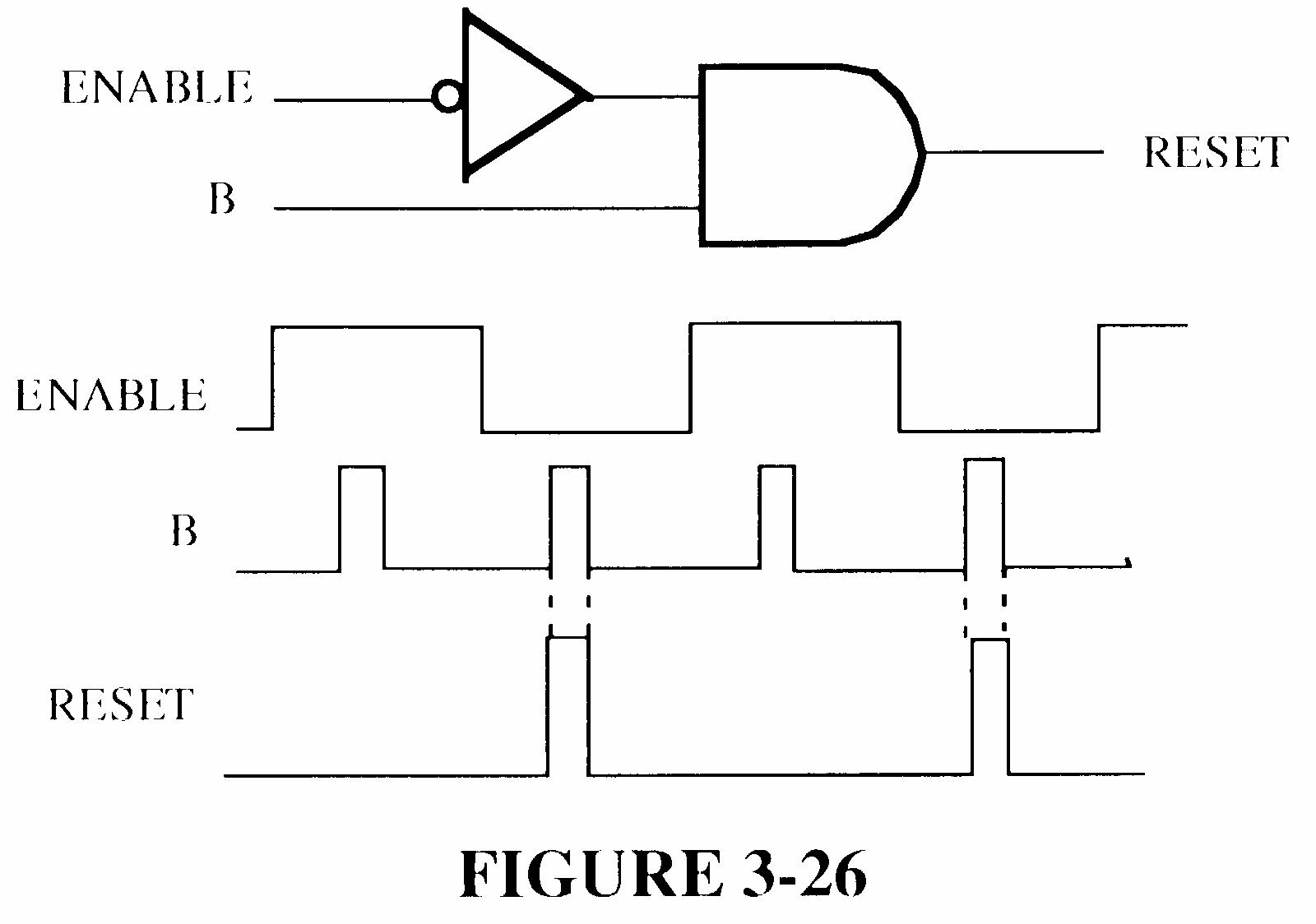
FIGURE 3-28
45. See Figure 3-29.
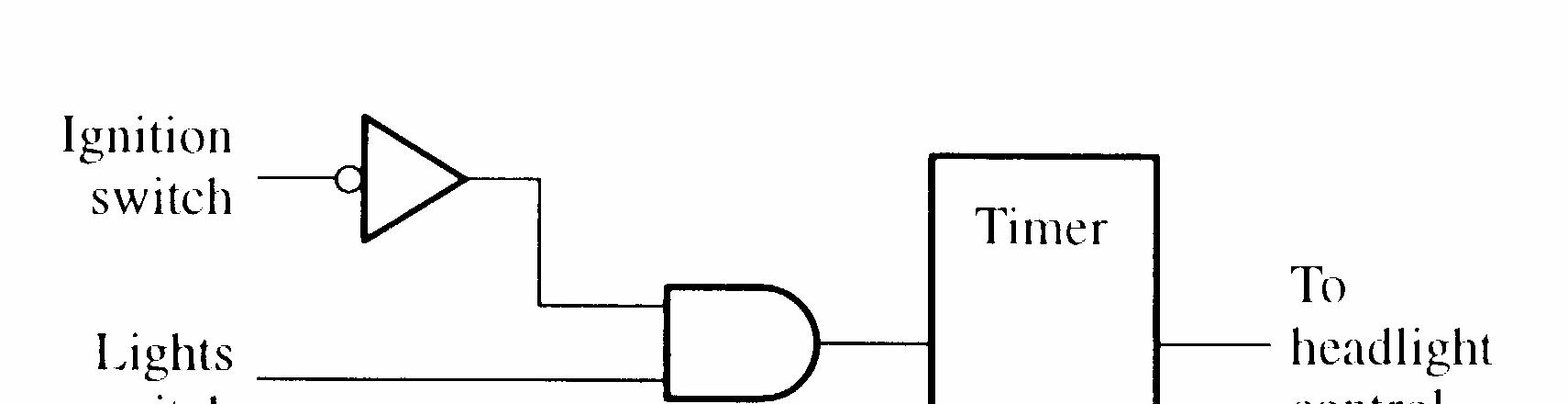
FIGURE 3-29
46. See Figure 3-30.
47. See Figure 3-31.
3-30

3-31
48. Input A shorted to output.
49. Inputs shorted together.
50. No fault.
51. Output open.
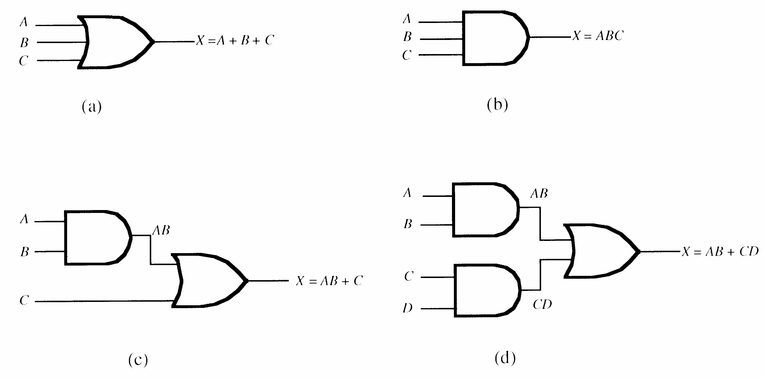
1. X = A + B + C + D This is an OR configuration.
2. Y = ABCDE
3. X = C B A + +
4. (a) 0 + 0 + 1 = 1 (b) 1 + 1 + 1 = 1 (c) 1
5. (a) AB = 1 when A = 1, B = 1
(b) BC A = 1 when A = 1, B = 0, C = 1
(c) A + B = 0 when A = 0, B = 0
(d) C B A + + = 0 when A = 1, B = 0, C = 1
(e) C B A + + = 0 when A = 1, B = 1, C = 0
(f) B A + = 0 when A = 1, B = 0
(g) BC A = 1 when A = 1, B = 0, C = 0
6. (a) X = (A + B)C + B
(b) X = C B A ) ( +
(c) X = BC A + AB
(d) X = (A + B)( A + B)
(e) X = (A + BC) ) ( C B +
7. (a) Commutative law of addition
(b) Commutative law of multiplication
(c) Distributive law
8. Refer to Table 4-1 in the textbook.
(a) Rule 9: A A =
(b) Rule 8: 0 = A A (applied to 1st and 3rd terms)
(c) Rule 5: A + A = A
(d) Rule 6: A A + = 1
(e) Rule 10: A + AB = A
(f) Rule 11: B A AB A + = + (applied to 1st and 3rd terms)
9. (a) AB = = + B A B A
(b) B A + = + = B A AB
(c) C B A + + = C B A
(d) C B A + + = ABC
(e) C B A + = + + = + ) ( ) ( C B A C B A
(f)
(g)
(h)
10. (a)
C B A + + + = + CD AB
= = + CD AB CD AB
)( ( ) )( (
A +
)( (
C B A + + = + + = + ) ( ) ( D C B A D C B A
(b) ) ( ) ( ) ( ) ( EF CD B A EF CD AB EF CD AB + + = + + = +
) )( ( F E D C B A + + + +
(c)
= + + + + D ABC D C B A ) (
= + + + =
A
C B A + + + + = + + + + D C B A D BC A
C
BC A D BC A D C B A + +
(d) ) )( ( ) )( (
C B A
(e) ) ( ) ( ) )( ( CD AB F E CD AB CD AB F E CD AB + + + + = + + = ) )( ( ) )( ( CD AB F E CD AB + + = ABCD F E D C AB + + + + ) )( (
11. (a) KLM HIJ EFG ABC KLM HIJ EFG ABC + + + = + ) )( ( ) )( ( = ) )( )( )( ( KLM HIJ EFG ABC KLM HIJ EFG ABC = + + + = ) )( )( )( ( M L K J I H G F E C B A + + + + + + + +
(b) BC CD BC A BC CD BC A BC CD BC A + = + = + + + ) )( ( ) )( ( ) ( = BC D ABC BC D ABC ABC BC D C ABC + + = + + = + + ) (1 ) ( = BC C AB +
(c) ) )( )( )( ( H G F E D C B A + + + + = H G F E D C B A = + + + + ) )( )( )( ( H G F E D C B A
12. (a) AB = X
(b) A = X
(c) A + B = X
(d) A + B + C = X
13. See Figure 4-1.
14. See Figure 4-2.
15. See Figure 4-3.
4-3
16. (a) See Figure 4-4(a). (b) See figure 4-4(b).
4-3
17. See Tables 4-1 and 4-2.
Table 4-1 INPUTS OUTPUT
Table 4-2 INPUTS OUTPUT
18. (a) X = A + B
20. (a)
)( ( = BC A + = + = + + + BC A BC B C A (1) ) (1
(b) (1) ) (1 AB DE C CD C AB DE ABC ABCD ABC AB = + + + = + + + = AB
(c)
(
A + C
(d) AABC AAB AABC AAB ABC AB A A + + + = + + ) )( ( = AB = + = + + + ) (1 0 0 C AB ABC AB
BC AC
AB C B A AB ) ( ) ( + + = + + + = + + + = C AB + = + ABC AB
(e) C B A AB
21. (a)
(c) ) )( )( (1 ) )( )( (
BC B BC B
+ + = ) )( ( ) )( ( ) )( ( D B
B C B B + +
+ +
+ = B(1 + C)(B + D) = B(B + D) = BB + BD = B + BD = B(1 + D) = B (d) CD B A D C AB ABCD CD AB CD AB ABCD ) ( ) ( ) ( ) ( + + + + = + + = BCD ACD D AB ABC ABCD + + + + = D AB ABC B A B CD D AB ABC B A AB CD + + + + = + + + + ) ( ) ( = AB CD + = + = + + = + + + ) ( ) (1
ABC CD D AB ABC A CD (e) ) ( )] ( [ AC BC C ABC ABABC AC BC C AB ABC + + = + + = ABC + 0(BC + AC) = ABC
AB
22. First develop the Boolean expression for the output of each gate network and simplify.
(a) See Figure 4-5.
(b) See Figure 4-6.
FIGURE 4-5
(c) See Figure 4-7.
FIGURE 4-6
FIGURE 4-7
X = D BC B A + No further simplification is possible.
(d) See Figure 4-8.
FIGURE 4-8
X = D AC B A + No further simplification is possible.
23. (a) B A BC AC + + = + + + = + + B A B B BC AC B C B A ) )( ( (b) BC AC + = + = + BCC AC C BC A ) ( (c) (A + C)(AB + AC) = AAB + AAC + ABC + ACC = AB + AC + ABC + ACC = (AB + AC)(1 + C) = AB + AC
24. (a) CD BCD A AB CDCD BCD A AB CD B A CD AB + + = + + = + + ) ( = CD AB + = + CD B A AB 1) (
(b) ABD ABBD BC AB BD BC AB + = + = + 0 ) ( = ABD (c) BD C B ABC A D C B AC B A ) ( ] ) ( [ + + + = + + + =
= + + + = A + BD
25. (a) The domain is A, B, C
The standard SOP is: ABC ABC ABC ABC + + +
(b) The domain is A, B, C
The standard SOP is: BC A BC A ABC + +
(c) The domain is A, B, C
The standard SOP is: ABC ABC ABC + +
26. (a) AB + CD = BCD A ABCD BCD A D ABC D ABC D ABC ABCD + + + + + +
(b) ABD = D ABC ABCD + (c) A + BD = D ABC D ABC BCD A D BC A D BC A D BC A + + + + + + ABCD D ABC ABCD D ABC + + +
27. (a) : ABC ABC BC A BC A + + + 101 + 100 + 111 + 011
(b) : BC A ABC ABC + + 111 + 101 + 001
(c) : BC A ABC ABC + + 111 + 110 + 101
28. (a) : BCD A ABCD BCD A D ABC D ABC D ABC ABCD + + + + + + 1111 + 1110 + 1101 + 1100 + 0011 + 0111 + 1011
(b) : D ABC ABCD + 1111 + 1101
(c) D ABC D ABC BCD A D BC A D BC A D BC A + + + + + + : ABCD D ABC ABCD D ABC + + + 1000 + 1001 + 1010 + 1011 + 1100 + 1101 + 1110 + 1111 + 0101 + 0111
29. (a) ) )( )( )( ( C B A C B A C B A C B A + + + + + + + +
(b) ) )( )( )( )( ( C B A C B A C B A C B A C B A + + + + + + + + + +
(c) ) )( )( )( )( ( C B A C B A C B A C B A C B A + + + + + +
31. (a) Table
Table
32. (a) Table 4-5
(b) Table 4-6
Table 4-7
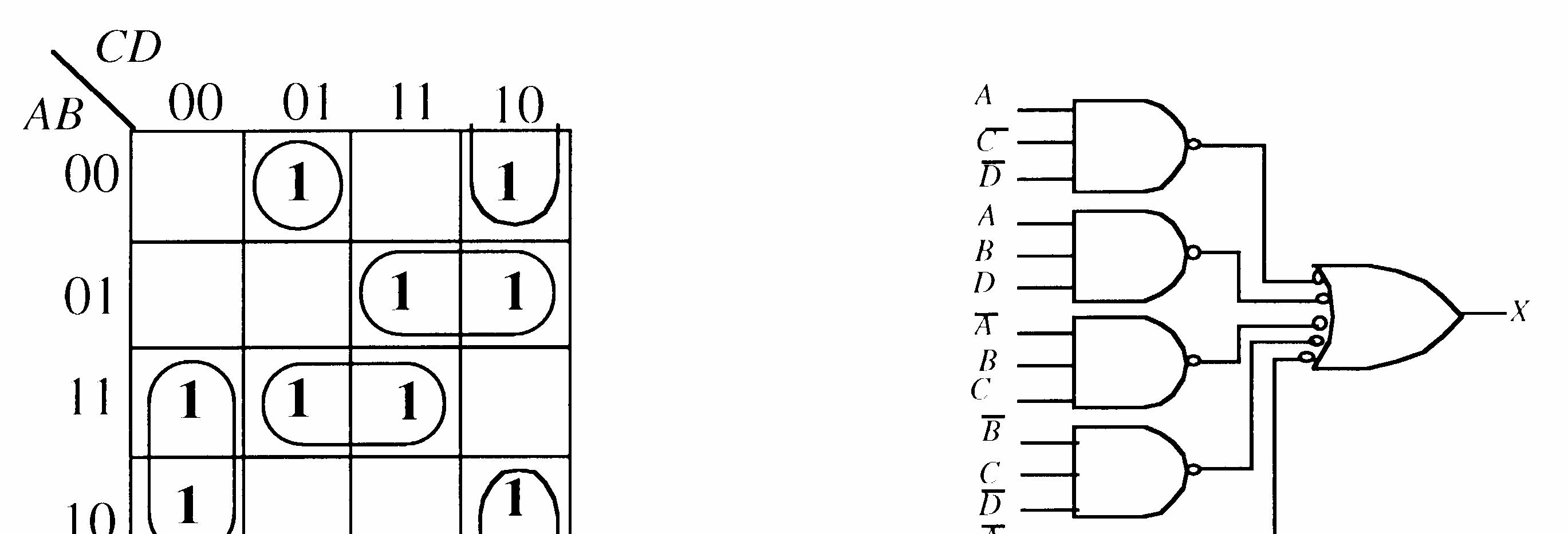
Table
34. (a) Table 4-9
35. (a) Table
36. (a) X = ABC BC A ABC ABC + + +
Table 4-10
Table
37. See Figure 4-9.
38. See Figure 4-10.
39. See Figure 4-11.
FIGURE 4-9
FIGURE 4-10
40. See Figure 4-12.
FIGURE 4-11
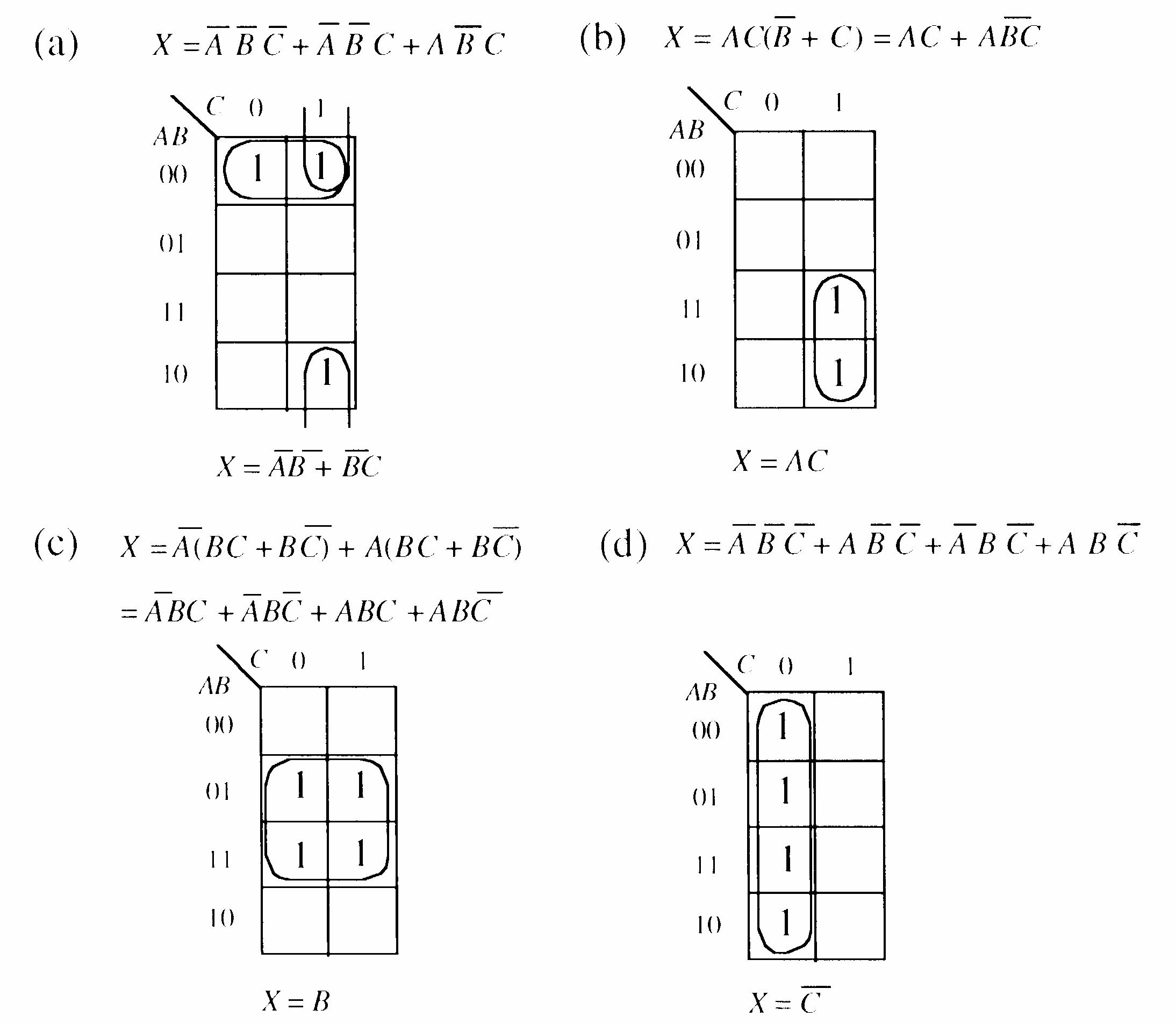
FIGURE 4-12
41. See Figure 4-13.
FIGURE 4-13
43. See Figure 4-14.
4-14
44. See Figure 4-15.
4-15
45. Plot the 1’s from Table 4-11 in the text on the map as shown in Figure 4-16 and simplify.
4-16
46. Plot the 1’s from Table 4-12 in the text on the map as shown in Figure 4-17 and simplify.
4-17
47. See Figure 4-18.
4-18
48. X ABCDEABCDE=+
See Figure 4-19.
FIGURE 4-19
49. See Figure 4-20.
FIGURE 4-20
50. See Figure 4-21.
4-21
51. entity AND_OR is port (A, B, C, D, E, F, G, H, I: in bit; X: out bit); end entity AND_OR; architecture Logic of AND_OR is begin
X <= (A and B and C) or (D and E and F) or (G and H and I); end architecture Logic;
52. The VHDL program:
entity SOP is port (A, B, C: in bit; X: out bit); end entity SOP; architecture Logic of SOP is begin
Y <= (A and not B and C) or (not A and not B and C) or (A and not B and not C) or (not A and B and C); end architecture Logic;
53. An LED display is more suitable for low-light conditions because LEDs emit light and LCDs do not.
54. The purpose of the invalid code detector is to detect the codes 1010, 1011, 1100, 1101, 1110, and 1111 to activate the display for letters.
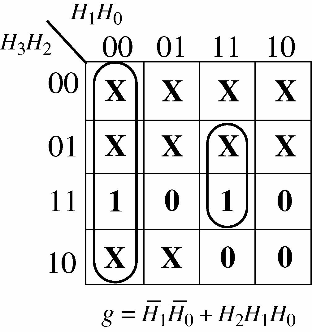
55. The standard SOP expression for segment c is:
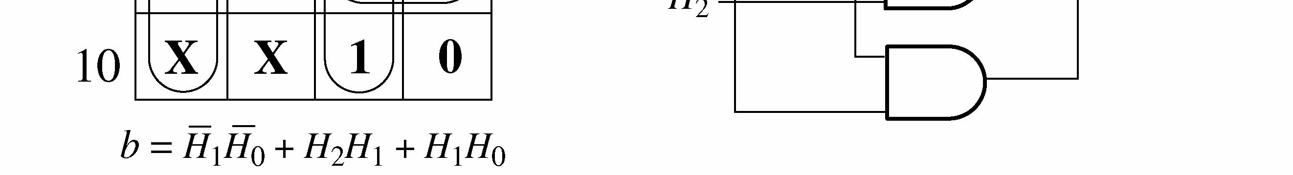
c = 321032103210 HHHHHHHHHHHH ++
This expression is minimized in Figure 4-22.
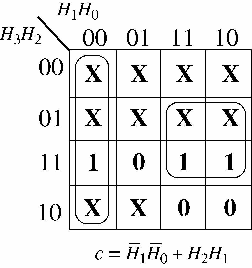
The standard expression requires three 4-input AND gates, one 3-input OR gate, and 3 inverters. The minimum expression requires two 2-input AND gates, one 2 input OR gate, and 2 inverters.
FIGURE 4-22
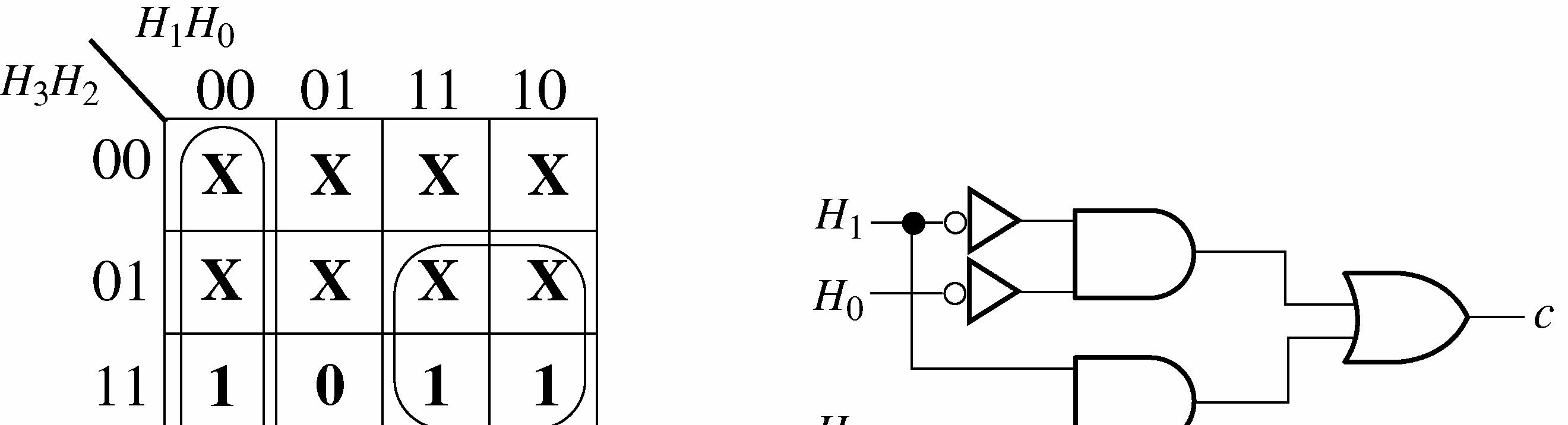
56. The standard SOP expression for segment d is:
d = 3210321032103210 HHHHHHHHHHHHHHHH +++ This expression is minimized in Figure 4-23.
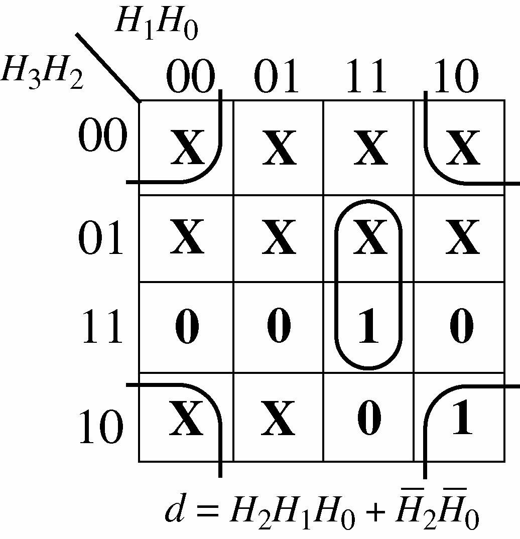
The standard expression requires four 4-input AND gates, one 4-input OR gate, and 3 inverters. The minimum expression requires one 2-input AND gates, one 3-input AND gate, one 2-input ORgate,and2inverters.
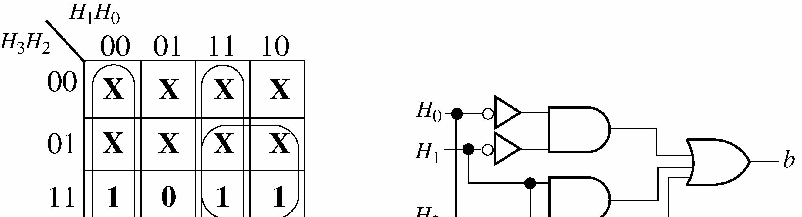
4-23
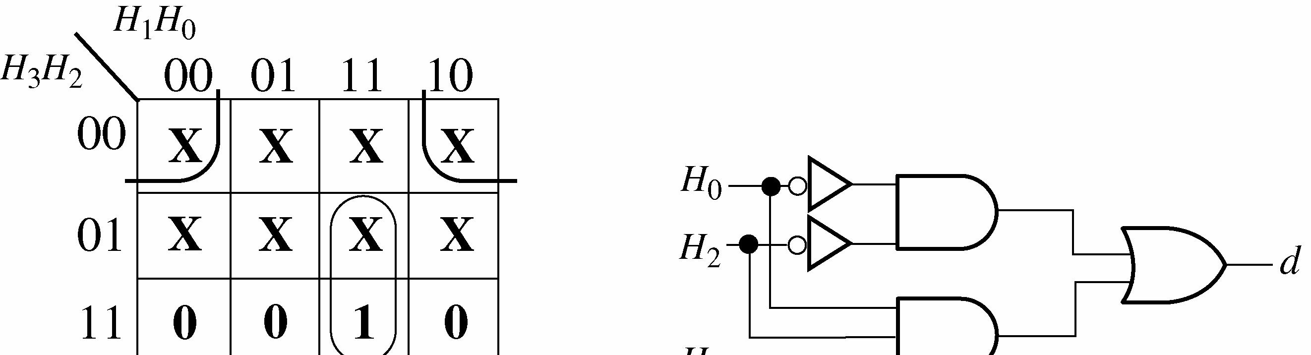
The standard SOP expression for segment e is: e = 32103210321032103210 HHHHHHHHHHHHHHHHHHHH ++++
This expression is minimized in Figure 4-24.
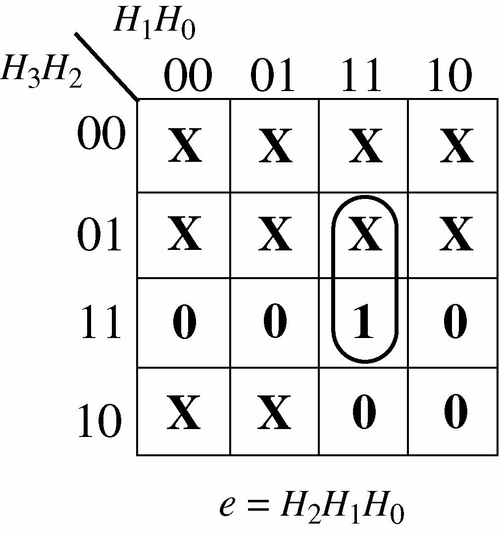
The standard expression requires five 4-input AND gates, one 5-input OR gate, and 3 inverters. The minimum expression requires one 3-input AND gate.
FIGURE 4-24
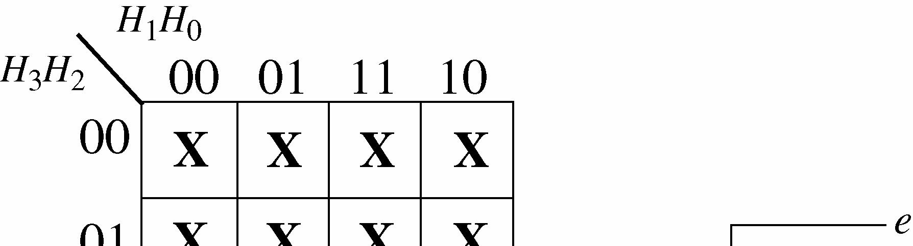
The standard SOP expression for segment f is: f = 3210321032103210 HHHHHHHHHHHHHHHH +++ This expression is minimized in Figure 4-25.
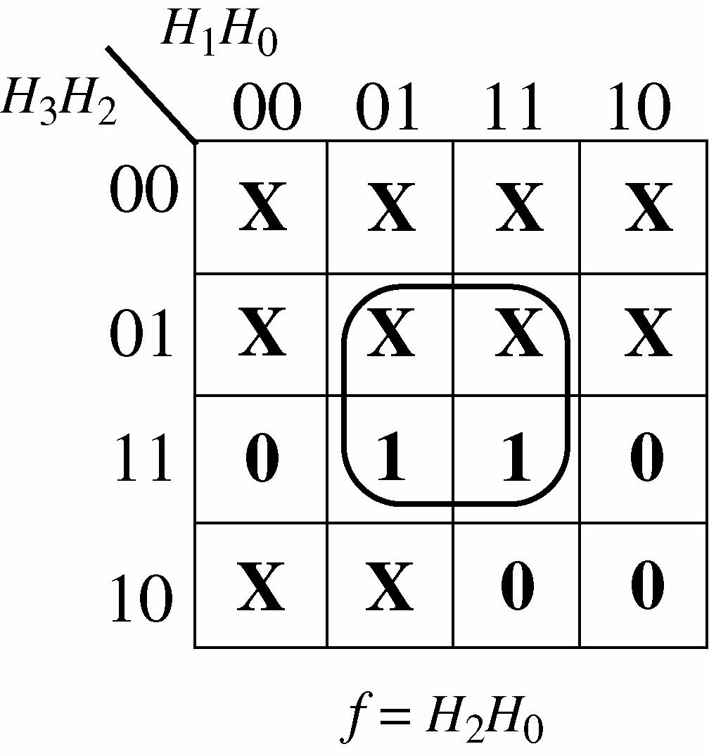
The standard expression requires four 4-input AND gates, one 4-input OR gate, and 3 inverters. The minimum expression requires one 2-input AND gate.
4-25
The standard SOP expression for segment g is: g = 3210321032103210 HHHHHHHHHHHHHHHH +++
This expression is minimized in Figure 4-26.
The standard expression requires four 4-input AND gates, one 4-input OR gate, and 3 inverters. The minimum expression requires one 2-input AND gates, one 3-input AND gate, one 2 input ORgate,and2inverters.
FIGURE 4-26
57. Connect the OR gate output for each segment to an inverter and then use the inverter output to drive the segment with a HIGH.
58. See Figure 4-27. F = 1111
The expression for segment a to include the letter F is: a = 3210321032103210 HHHHHHHHHHHHHHHH +++ The expression is minimized in Figure 4-27.
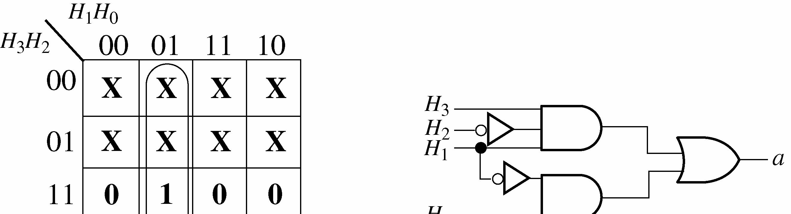
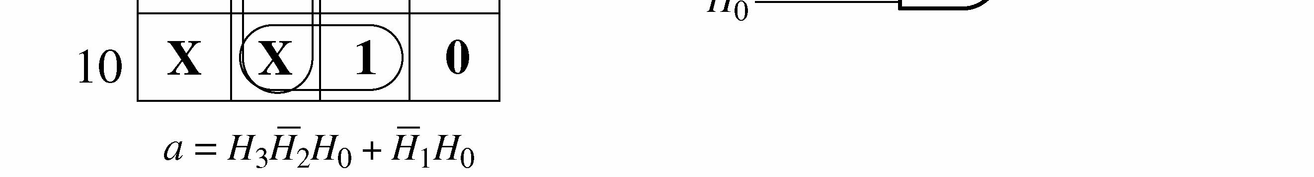
FIGURE 4-27
59. See Figure 4-28. Segment b is used for letters A and d b = 32103210 HHHHHHHH +
4-28
See Figure 4-29. Segment c is used for letters A, b, and d c = 321032103210 HHHHHHHHHHHH ++

4-29
See Figure 4-30. Segment d is used for b, C, d, and E d = 3210321032103210 HHHHHHHHHHHHHHHH +++

4-30
See Figure 4-31. Segment e is used for A, b, C, d, E, and F e = 321032103210321032103210 HHHHHHHHHHHHHHHHHHHHHHHH +++++
Since segment e is active-LOW for all letters, e = 0.
FIGURE 4-31
See Figure 4-32. Segment f is used for A, b, C, E, and F f = 32103210321032103210 HHHHHHHHHHHHHHHHHHHH ++++
4-32
See Figure 4-33. Segment g is used in A, b, d, E, and F g = 32103210321032103210 HHHHHHHHHHHHHHHHHHHH ++++

60. The invalid code detector must disable the display when any numerical input (0-9) occurs. A HIGH enables the display and a LOW disables it. A circuit that detects the numeric codes and produces a LOW is shown in Figure 4-34.
61. Input A inverter output open.
62. Input A of segment e OR gate open.
63. Segment b OR gate output open.
1. See Figure 5-1.
2. (a) X = AC A AB + +
(b) X = D DB ACD AB + +
3. (a) X = ABB
(b) X = AB + B
(c) X = B A +
(d) X = (A + B) + AB
(e) X = ABC
(f) X = ) )( ( C B B A + +
4. See Figure 5-2 for the circuit corresponding to each expression.
(a) X = (A + B)(C + D) = AC + AD + BC + BD
(b) X = BCD ACD CCD B A CD ABC CD ABC + = + = = + ) ( ) )( ( (c) X = (AB + C)D + E = ABD + CD + E
X =
X =
X =
(
5. (a) X = ABB A B X 0 0 1 1 0 1 0 1 0 0 0 1 (d) X = (A + B) + AB A B X 0 0 1 1 0 1 0 1 0 1 1 1 (b) X = AB + B A B X 0 0 1 1 0 1 0 1 0 1 0 1
X = ABC A B C X
X = B A + A B X
X =
6. (a) X
(A + B)(C + D) A
)
X = D BC B A + + ) )( ( A B C D X 0 0 0 0 0 0 0 0 1 1 1 1 1 1 1 1 0 0 0 0 1 1 1 1 0 0 0 0 1 1 1 1 0 0 1 1 0 0 1 1 0 0 1 1 0 0 1 1 0 1 0 1 0 1 0 1 0 1 0 1 0 1 0 1 1 1 1 1 1 1 1 1 0 1 0 1 1 1 1 1
For all other entries X = 0. X = don’t care An abbreviated table is shown because there are 256 combinations.
8. Let G = guard, S = switch, M = motor temp, and P = power. See Figure 5-3. P = GSMS +
9. X = ABCDEFGH +
10. See Figure 5-4.
11. See Figure 5-5.
12. See Figure 5-6.
See Figure 5-7.
See Figure 5-8.
5-8
15. X = AB + ABC = AB(1 + C) = AB
Since C is a don’t care variable, the output depends only on A and B as shown by the twovariable truth table above which is implemented with the AND gate in Figure 5-9.
5-9
16. X = C BC B A C C B AB C C B AB C C B AB ) )( ( ) )( ( ) )( ( ) )( ( + = + = + = + + = C B = + = + = + 1) ( ) ( A BC BC BC A C BC BC A
See Figure 5-10.
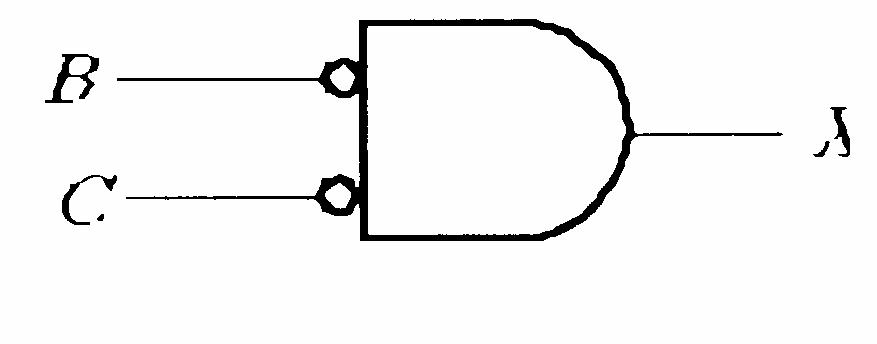
FIGURE 5-10
17. (a) X = BC AB + No simplification. See Figure 5-11.
The output is dependent only on B and C. The value of A does not matter. The NOR gate behaves as a negative-AND.
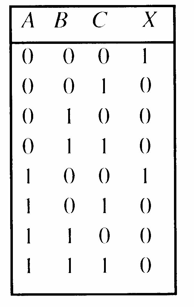
FIGURE 5-11
(b) X = () ABCABAC +=+
No simplification. Equation can be expressed in another form, as indicated in Figure 5-12.
FIGURE 5-12
(c) X = ) ( B B A B A AB + = + = A
A direct connection from input to output. No gates required. X ABBC=+
(d) X = BG BEF C B A G EF B ABC + + + + = + + ) ( = G EF B C A + + + + = + + + + G B BEF C A
See Figure 5-13.
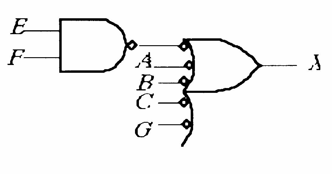
FIGURE 5-13
(e) X = A(BC(A + B + C + D)) = ABCA + ABCB + ABCC + ABCD = ABC + ABC + ABC + ABCD = ABC + ABC(1 + D) = ABC + ABC = ABC
See Figure 5-14. (f) X = )
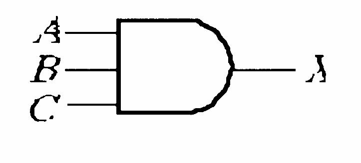
FIGURE 5-14
DE BC C AB FG E DE C B + + + = + + = EFG BC DE BC EFG AB DE ABC + + + = FG E BC FG E AB A DE BC + + + 1) ( = FG E BC FG E AB E D BC + +
See Figure 5-15.
FIGURE 5-15
E
( ) )( ( C B A
18. (a) X = ) )( ( BE ACD B A CD AB + + + + = ) ( E B ACD B A CD AB + + + + = E B A CD B B A E B A B A CD AB + + + = + + + ) ( = CD A + = + + = + + CD E B A CD E B A A ) (1
See Figure 5-16.
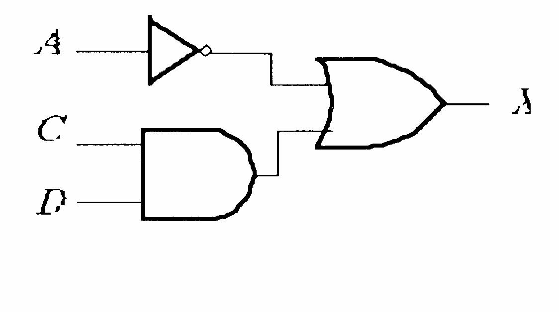
FIGURE 5-16
(b) X = F A DEF D ABC AF F E D D ABC + + + = + + = E D F D C B A + + +
See Figure 5-17.
See Figure 5-18. X X X
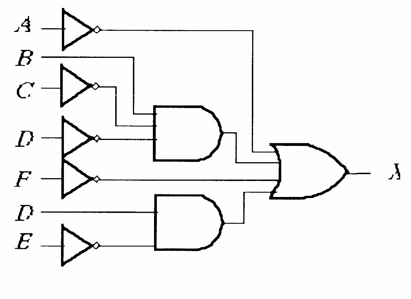
FIGURE 5-17
(c) X = E AC D AC AB + + = + + = + + ) ( )) ( ( E C D C B A E D C B A
FIGURE 5-18
19. The SOP expressions are developed as follows and the resulting circuits are shown in Figure 5-19.
(a) X = (A + B)(C + D) = AC + AD + BC + BD
(b) X = BCD ACD + = + = = + CCD B A CD ABC CD ABC ) ( ) )( (
(c) X = (AB + C)D + E = ABD + CD + E
(d) X = ()()()() ABBCDABBCDABBCD ++=++=+++ = D B A + + = + + + D C B A ) (1
(e) X = E D C ABD + + = + + = + + E D C AB E D C AB ) ( ) (
(f) X = ) ( ) ( ) )( ( ) )( ( GHG EF CD AB GH EF CD AB GH EF CD AB + + + = + + = + + = ()()()()()()()() ABCDEFGHABCDEFGH +=+++++ = +++++++ ACBCADBDEGFGEHFH
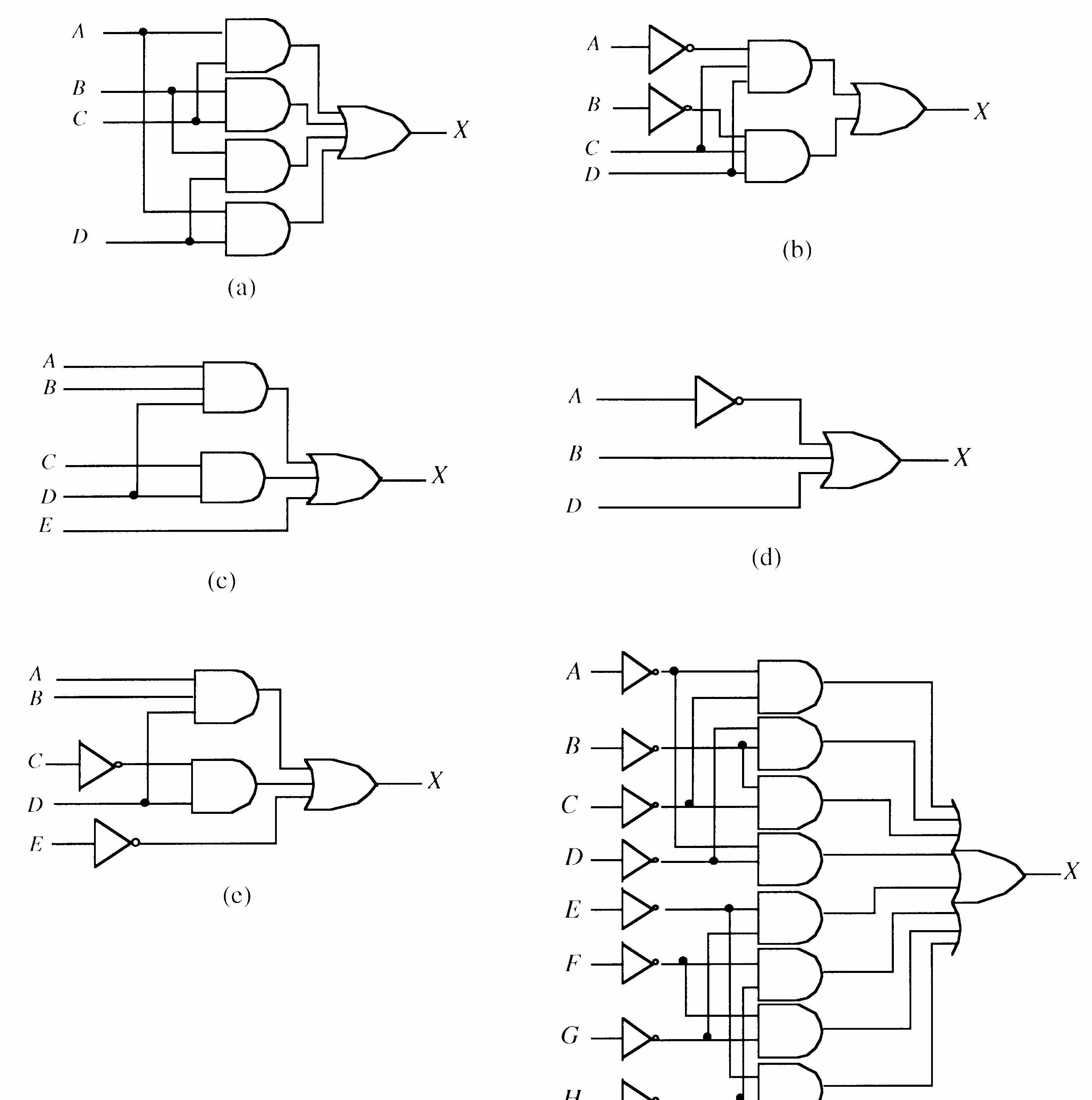
FIGURE 5-19
5-3
20. See Figure 5-20.
See Figure 5-21.
22. See Figure 5-22.
23. See Figure 5-23.
Section 5-4 Combinational Logic Using NAND and NOR Gates
24. (a) X = ABC
See Figure 5-24.
(b) X = ABC
See Figure 5-25.
(c) X = A + B
See Figure 5-26.
(d) X = C B A + +
See Figure 5-27.
(e) X = CD AB +
See Figure 5-28.
(f) X = (A + B)(C + D)
See Figure 5-29.
FIGURE 5-29
(g) X = ] ) ( [ BCE AB DE C AB + +
See Figure 5-30.
See Figure 5-29. X
5-28
FIGURE 5-30
25. (a) X = ABC
See Figure 5-31.
FIGURE 5-31
(c) X + A + B
See Figure 5-33.
FIGURE 5-33
(e) X = CD AB +
See Figure 5-35.
5-35
(b) X = ABC
See Figure 5-32.
5-32
(d) X = C B A + +
See Figure 5-34.
5-34
(f) X = (A + B)(C + D)
See Figure 5-36.
FIGURE 5-36
(g) X = ] ) ( [ BCE AB DE C AB + +
See Figure 5-37.
26. (a) X = AB
See Figure 5-38.
5-38
(c) X = AB + C
See Figure 5-40.
5-37
See Figure 5-41. X X X X X
(b) X = A + B
See Figure 5-39.
5-39
5-40
(d) X = ABC + D
5-41
(e) X = A + B + C
See Figure 5-42.
(f) X = ABCD
See Figure 5-43.
5-43
5-42
(g) X = A(CD + B) = ACD + AB
See Figure 5-44.
FIGURE 5-44
(h) X = AB(C + DEF) + CE(A + B + F) = ABC + ABDEF + CEA + CEB + CEF
See Figure 5-45.
5-45
27. (a) X = BC AB +
See Figure 5-46.
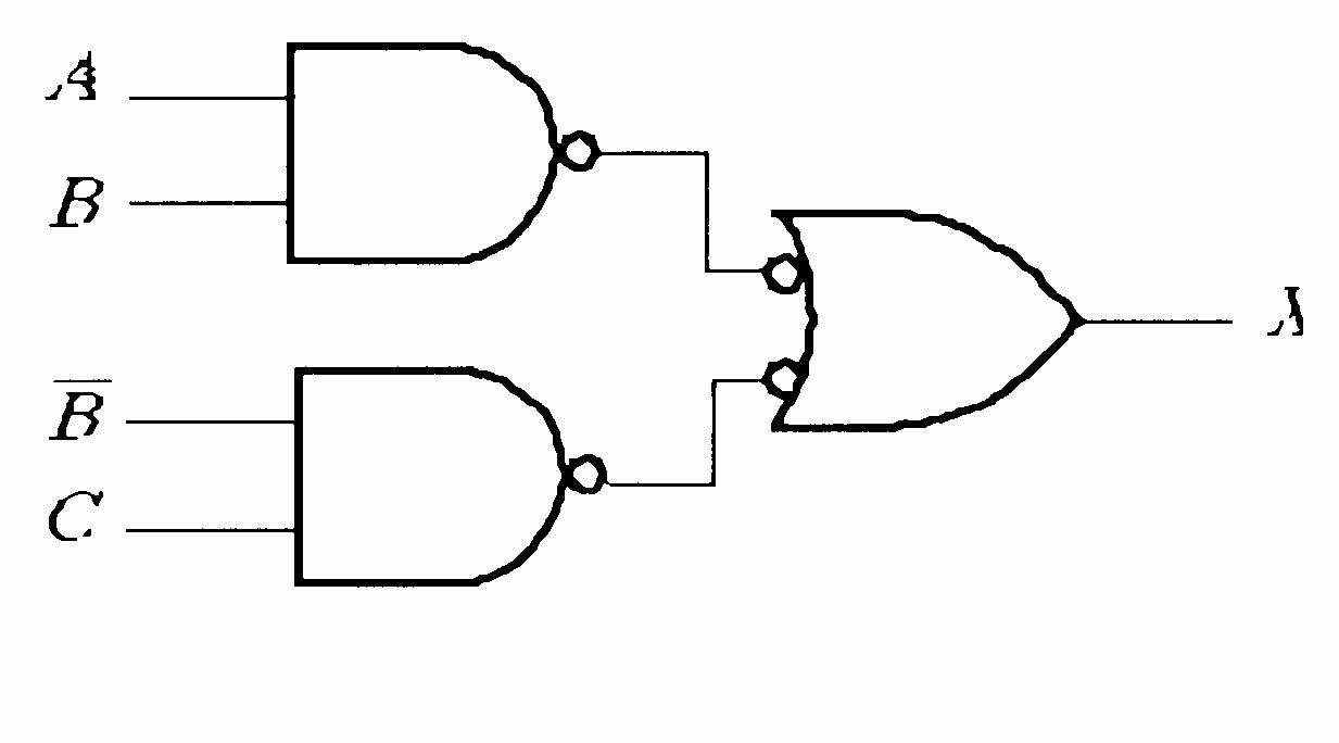
FIGURE 5-46
(c) X = AB B A +
See Figure 5-48.
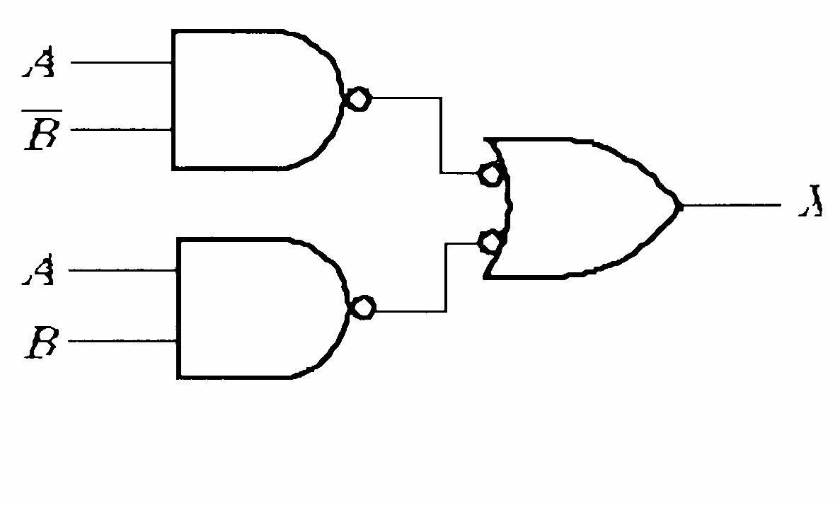
FIGURE 5-48
(b) X = AC AB + = + ) ( C B A
See Figure 5-47.
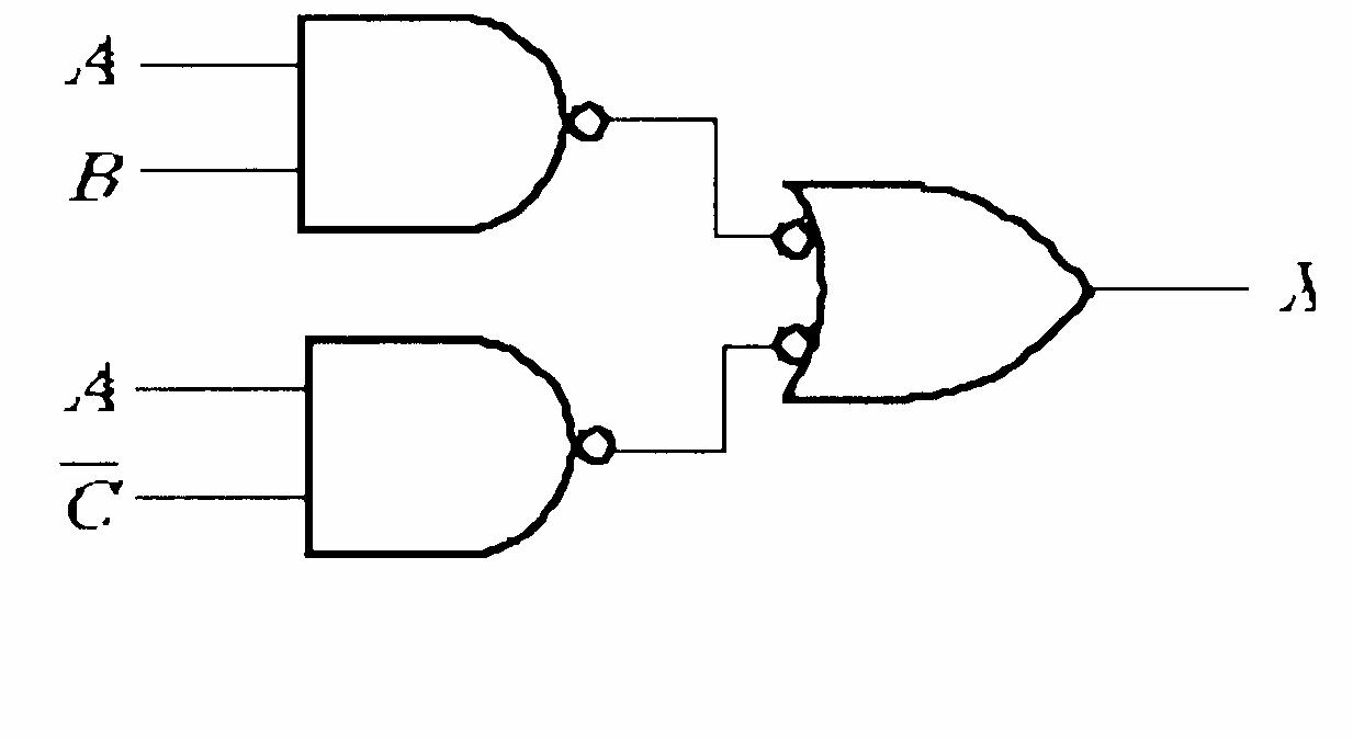
FIGURE 5-47
(d) X = BG BEF C B A + + + + = + + ) ( G EF B ABC
See Figure 5-49. X X X X
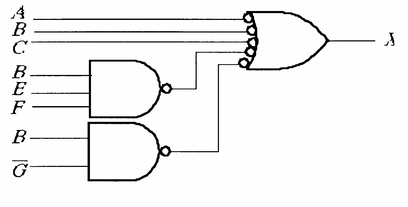
FIGURE 5-49
See Figure 5-50.
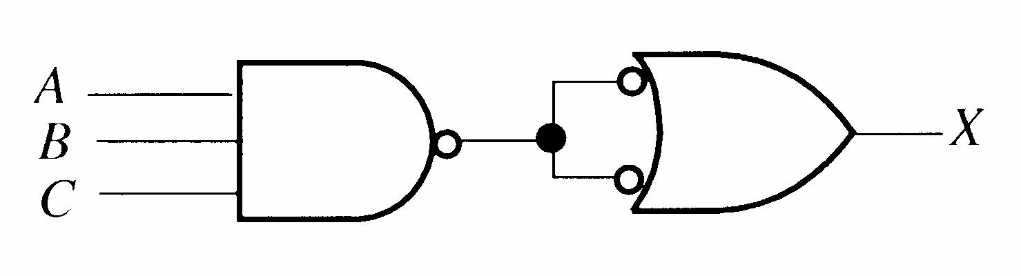
FIGURE 5-50
See Figure 5-51.
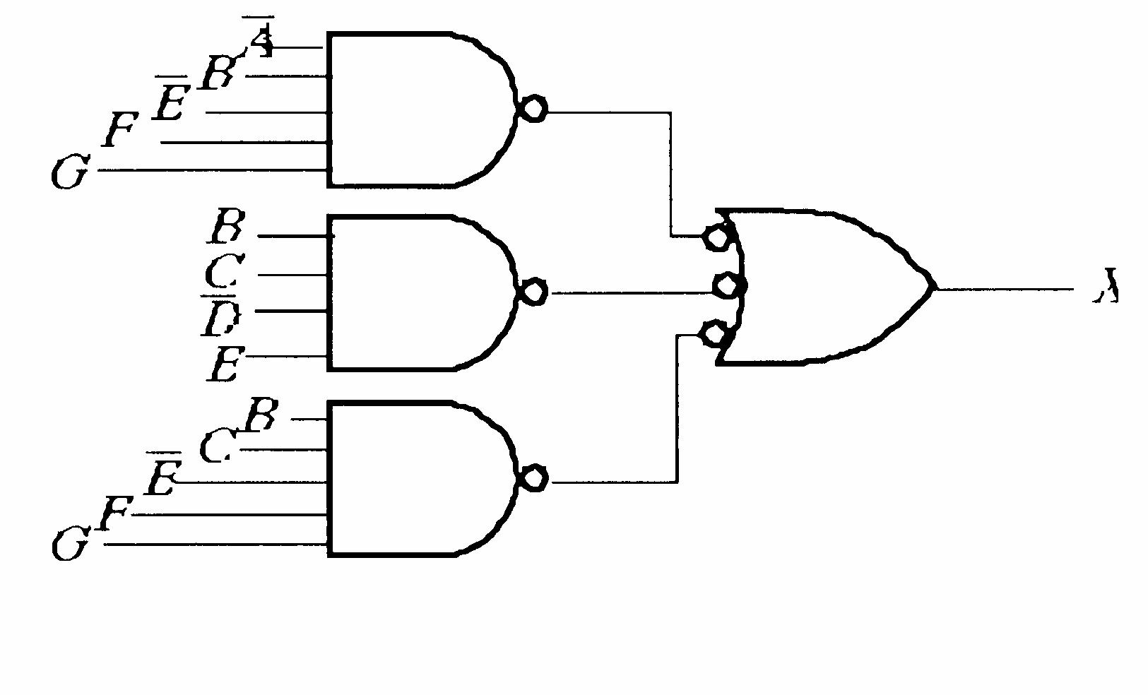
FIGURE 5-51
Section 5-5 Logic Circuit Operation with Pulse Waveform Inputs
28. X = B AB B B A = + + = 0 The output X is always LOW.
29. X = B A + = + + = B B A B AB ) ( See Figure 5-52.
5-52
30. X is HIGH when ABC are all HIGH or when A is HIGH and B is LOW and C is LOW or when A is HIGH and B is LOW and C is HIGH.
X = ABC ABC ABC + +
See Figure 5-53.
5-53
31. X is HIGH when A is HIGH, B is LOW, and C is LOW. We do not know if X is HIGH when all inputs are HIGH.
X = BC A
See Figure 5-54.
5-54
32. See Figure 5-55.
FIGURE 5-55
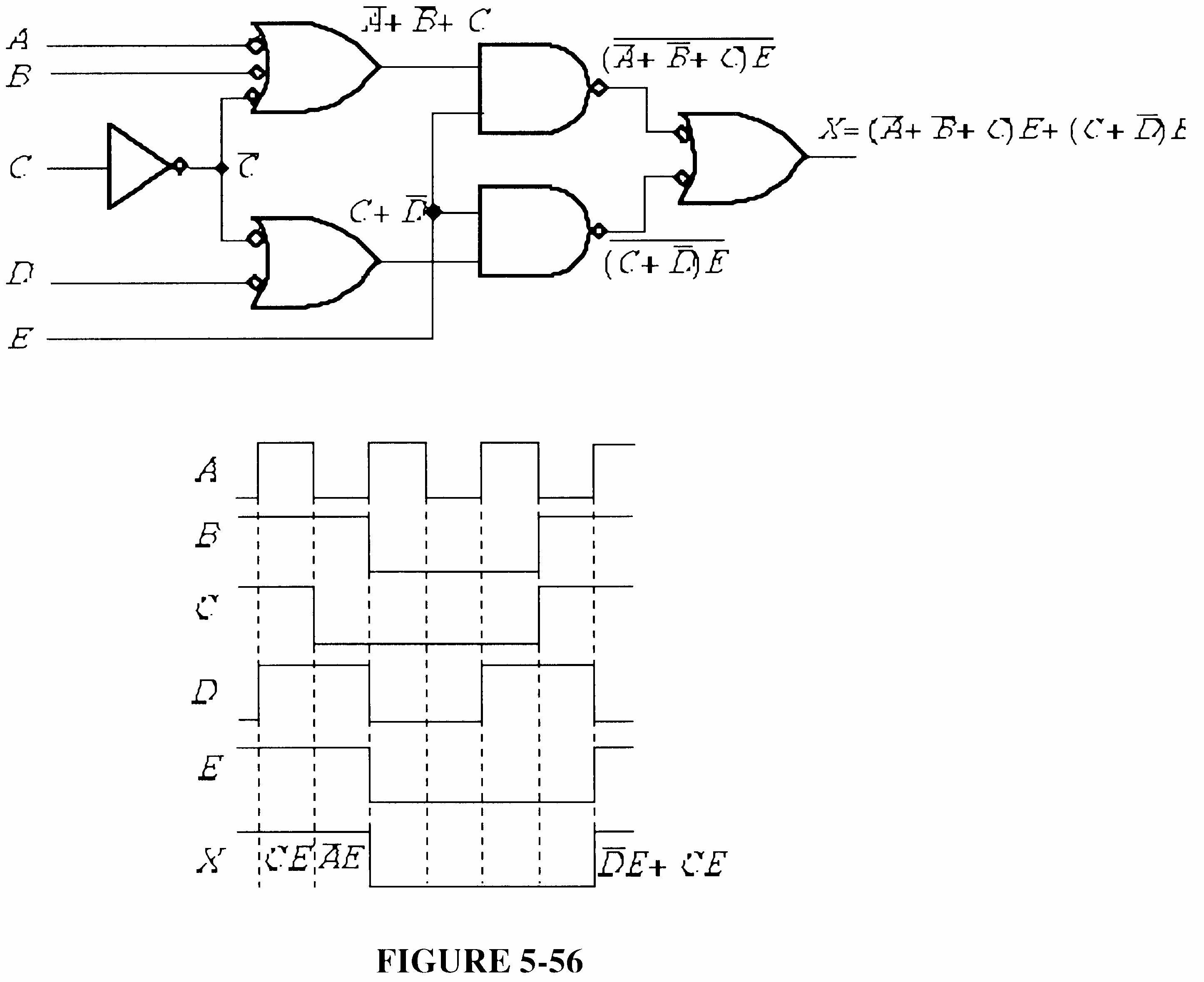
33. The output pulse is sufficiently wide. It is greater than 25 ns. A maximum is not specified. See Figure 5-56.
FIGURE 5-56
34. X = CD AB + = ABCD
X is HIGH only when ABCD are all HIGH. This does not occur in the waveforms, so X should remain LOW. The output is incorrect.
35. X = E D ABC +
Since X is the same as the G3 output, either G1 or G2 has failed with its output stuck LOW
36. X = AB + CD + EF
X does not go HIGH when C and D are HIGH. G2 has failed with the output open or stuck HIGH or the corresponding input to G4 is open.
37. See Figure 5-57.
X = ) )( )( ( F E D C B A F E D C B A = + + = (A + B)(C + D)(E + F)
Since X does not go HIGH when C or D is HIGH, the output of gate G2 must be stuck LOW
(a)
See Figure 5-58.
(b) X = ) (1 ) ( C D E C D E E + + = + + = E
Waveform X is the same as waveform E, in Figure 5-58. Since this is the correct waveform, the open output of gate G3 does not show up for this particular set of input waveforms.
Again waveform X is the same as waveform E. As strange as it may seem, the shorted input to G5 does not affect the output for this particular set of input waveforms.
Conclusion: the two faults are not indicated in the output waveform for these particular inputs.
40. TP = D C B A +
The output of the D C gate is stuck LOW. See Figure 5-59.
FIGURE FIGURE55-62 -59
41. X <= A and B and C
42. entity Circuit5_54b is port (A, B, C, D: in bit; X: out bit); end entity Circuit5_54b; architecture LogicFunction of Circuit5_54b is begin
X <= not(not A and B) or (not A and C and D) or (D and B and not D); end architecture LogicFunction;
43.(e) entity Circuit5_55e is port (A, B, C: in bit; X: out bit); end entity Circuit5_55e; architecture LogicFunction of Circuit5_55e is begin
X <= (not A and B) or B or (B and not C) or (not A and not C) or (B and not C) or not C; end architecture LogicFunction;
(f) entity Circuit5_55f is port (A, B, C: in bit; X: out bit); end entity Circuit5_55f; architecture LogicFunction of Circuit5_55f is begin X <= (A or B) and (not B or C); end architecture Logic Function;
44. See Figure 5-60 for input/output, gate, and signal labeling.
--Program for the logic circuit in Figure 5-60 (textbook Figure 5-56(d)) entity (Circuit5_56d is port (IN1, IN2, IN3, IN4: in bit; OUT: out bit); end entity Circuit5_56d; architecture LogicOperation of Circuit5_56d is --Component declaration for inverter component Inverter is port (A: in bit; X: out bit); end component Inverter; --Component declaration for NOR gate component NORgate is port (A, B: in bit; X: out bit); end component NOR gate; --Component declaration for NAND gate component NANDgate is port (A, B: in bit; X: out bit); end component NANDgate; signal G1OUT, G2OUT, G3OUT, G4OUT, G5OUT: bit; begin
G1: Inverter port map (A => IN1, X => G1OUT);
G2: NORgate port map (A => G1OUT, B => IN2, X => G2OUT);
G3: NAND gate port map (A => IN2, B => IN3, X => G3OUT);
G4: NANDgate port map (A => G2OUT, B => G3OUT, X => G4OUT);
G5: NORgate port map (A => G4OUT, B => IN4, X => G5OUT);
G6: Inverter port map (A => G5OUT, X => OUT); end architecture LogicOperation;
45. See Figure 5-61 for input/output, gate, and signal labeling.
5-59
FIGURE5-61
--Program for the logic circuit in Figure 5-61 (textbook Figure 5-56(f)) entity Circuit5_56f is port (IN1, IN2, IN3, IN4, IN5, IN6, IN7, IN8: in bit; OUT: out bit); end entity Circuit5_56f; architecture LogicFunction of Circuit5_56f is --Component declaration for NAND gate component NANDgate is port (A, B: in bit; X: out bit); end component NANDgate; signal G1OUT, G2OUT, G3OUT, G4OUT, G5OUT, G6OUT: bit; begin
G1: NANDgate port map (A => IN1, B => IN2, X => G1OUT);
G2: NANDgate port map (A => IN3, B => IN4, X => G2OUT);
G3: NANDgate port map (A => IN5, B => IN6, X => G3OUT);
G4: NANDgate port map (A => IN7, B => IN8, X => G4OUT);
G5: NANDgate port map (A => G1OUT, B => G2OUT, X => G5OUT);
G6: NANDgate port map (A => G3OUT, B => G4OUT, X => G6OUT);
G7: NANDgate port map (A => G5OUT, B => G6OUT, X => OUT); end architecture LogicFunction;
46. X = ABC BC A ABC BC A + + + + ABC
This is the SOP expression for the function in Table 5-8 of the textbook. The following program applies the data flow approach for this logic function.
--Program for Table5_8 SOP logic entity Table5_8 is port (A, B, C: in bit; X: out bit); end entity Table5_8; architecture LogicOperation of Table5_8 is begin
X <= (not A and not B and not C) or (not A and B and not C) or (A and not B and not C) or (A and B and not C) or (A and B and C); end architecture LogicOperation;
47. --Program for textbook Figure 5-66 data flow approach
entity Fig5_66 is port (A, B, C, D, E: in bit; X: out bit);
end entity Fig5_66; architecture DataFlow of Fig5_66 is begin X <= (A and B and C) or (D and not E) end architecture DataFlow;
See Figure 5-62 for the circuit in textbook Figure 5-66 modified for the structural approach.
FIGURE 5-58
--Program for textbook Figure 5-66 structural approach
entity Fig5_66 is
port (IN1, IN2, IN3, IN4, IN5: in bit; OUT: out bit);
end entity Fig5_66; architecture Structure of Fig5_66 is
--Component declaration for AND gate component AND_gate is port (A, B: in bit; X: out bit); end component AND_gate;
--Component declaration for OR gate component OR_gate is port (A, B: in bit; X: out bit); end component OR_gate;
--Component declaration for Inverter component Inverter is port (A: in bit; X: out bit); end component Inverter; signal G1OUT, G2OUT, G3OUT, INVOUT: bit; begin
G1: AND_gate port map (A => IN1, B => IN2, X => G1OUT);
G2: AND_gate port map (A => G1OUT, B => IN3, X => G2OUT); INV: Inverter port map (A => IN5, X => INVOUT);
G4: OR_gate port map (A => G2OUT, B => G3OUT, X => OUT); end architecture Structure; FIGURE5-62
G3: AND_gate port map (A => IN4, B => INVOUT, X => G3OUT);
48. --Program for textbook Figure 5-70 data flow approach entity Fig5_70 is port (A, B, C, D, E: in bit; X: out bit); end entity Fig5_70; architecture DataFlow of Fig5_70 is begin
X <= (not A or not B or C) and E or (C or not D) and E; end architecture DataFlow;
See Figure 5-63 for the circuit in textbook Figure 5-70 labeled for the structural approach.
--Program for textbook Figure 5-70 structural approach
entity Fig5_70 is port (IN1, IN2, IN3, IN4, IN5: in bit; OUT: out bit); end entity Fig5_70; architecture Structure of Fig5_70 is --Component declaration for 3-input NAND gate component NAND_gate3 is port (A, B, C: in bit; X: out bit); end component NAND_gate3; --Component declaration for 2-input NAND gate component NAND_gate2 is port (A, B: in bit; X: out bit); end component NAND_gate2; --Component declaration for Inverter component Inverter is port (A: in bit; X: out bit); end component Inverter; signal G2OUT, G3OUT, G4OUT, G5OUT, INVOUT: bit; begin
G1: NAND_gate2 port map (A => G2OUT, B => G4OUT, X => OUT);
G2: NAND_gate2 port map (A => G3OUT, B => IN5, X => G2OUT); INV: Inverter port map (A => IN3, X => INVOUT);
G3: NAND_gate3 port map (A => IN1, B => IN2, C => INVOUT, X => G3OUT);
G4: NAND_gate2 port map (A => IN5, B => G5OUT, X => G4OUT);
G5: NAND_gate2 port map (A => INVOUT, B => IN4, X => G5OUT); end architecture Structure;
49. From the VHDL program, the logic expression is stated as a Boolean expression as follows:
X = () ABACADBCBDDC +++++ = (()()()()()()) ABACADBCBDDC ++++++
+ +
= ) )( )( )( )( )( (
The truth table is:
50. --Program for textbook Figure 5-72 data flow approach entity Fig5_72 is port (A1, A2, B1, B2: in bit; X: out bit); end entity Fig5_72; architecture LogicCircuit of Fig5_72 is begin X <= (A1 and A2) or (A2 and not B1) or (not B1 and not B2) or (not B2 and A1); end architecture LogicCircuit;
51. The AND gates are numbered top to bottom G1, G2, G3, G4. The OR gate is G5 and the inverters are, top to bottom. G6 and G7. Change A1, A2, B1, B2 to IN1, IN2, IN3, IN4 respectively. Change X to OUT.
entity Circuit5_72 is port (IN1, IN2, IN3, (IN4: in bit; OUT: out bit); end entity Circuit 5_72; architecture Logic of Circuit 5_72 is component AND_gate is port (A, B: in bit; X: out bit); end component AND_gate; component OR_gate is port (A, B, C, D: in bit; X: out bit); end component OR_gate; component Inverter is port (A: in bit; X: out bit); end component Inverter; signal G1OUT, G2OUT, G3OUT, G4OUT, G5OUT, G6OUT, G7OUT: bit; begin
G1: AND_gate port map (A => IN1, B => IN2, X => G1OUT);
G2: AND_gate port map (A => IN2, B => G6OUT, X => G2OUT);
G3: AND_gate port map (A => G6OUT, B => G7OUT, X => G3OUT);
G4: AND_gate port map (A => G7OUT, B => IN1, X => G4OUT);
G5: OR_gate port map (A => G1OUT, B => G2OUT, X => G3OUT, D => G4OUT, X => OUT);
G6: Inverter port map (A => IN3, X => G6OUT);
G7: Inverter port map (A => IN4, X => G7OUT); end architecture Logic;
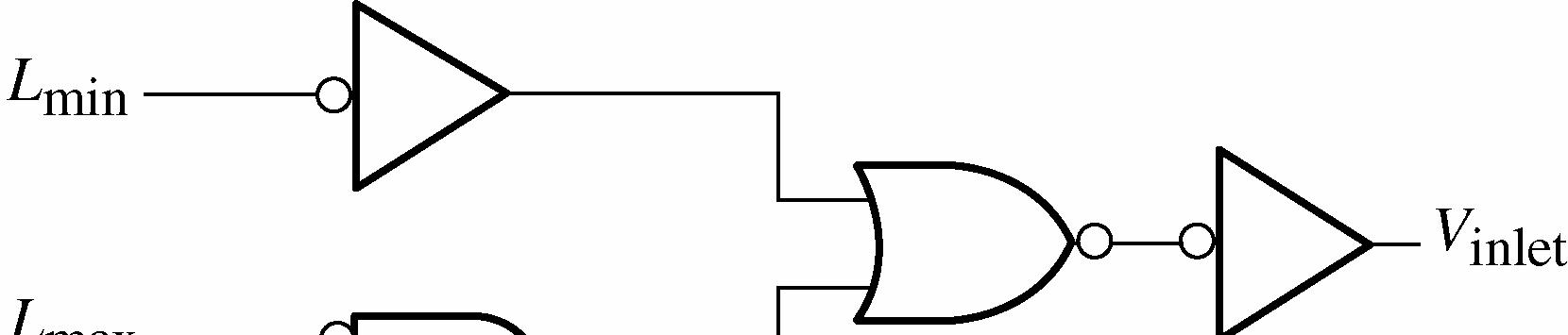
52. inletminmaxinlet VLLF =+ See Figure 5-64.

53. outletmininlet VLFT = See Figure 5-65.
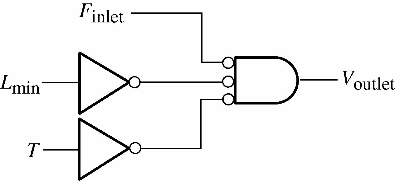
FIGURE 5-65
54. See Figure 5-66.
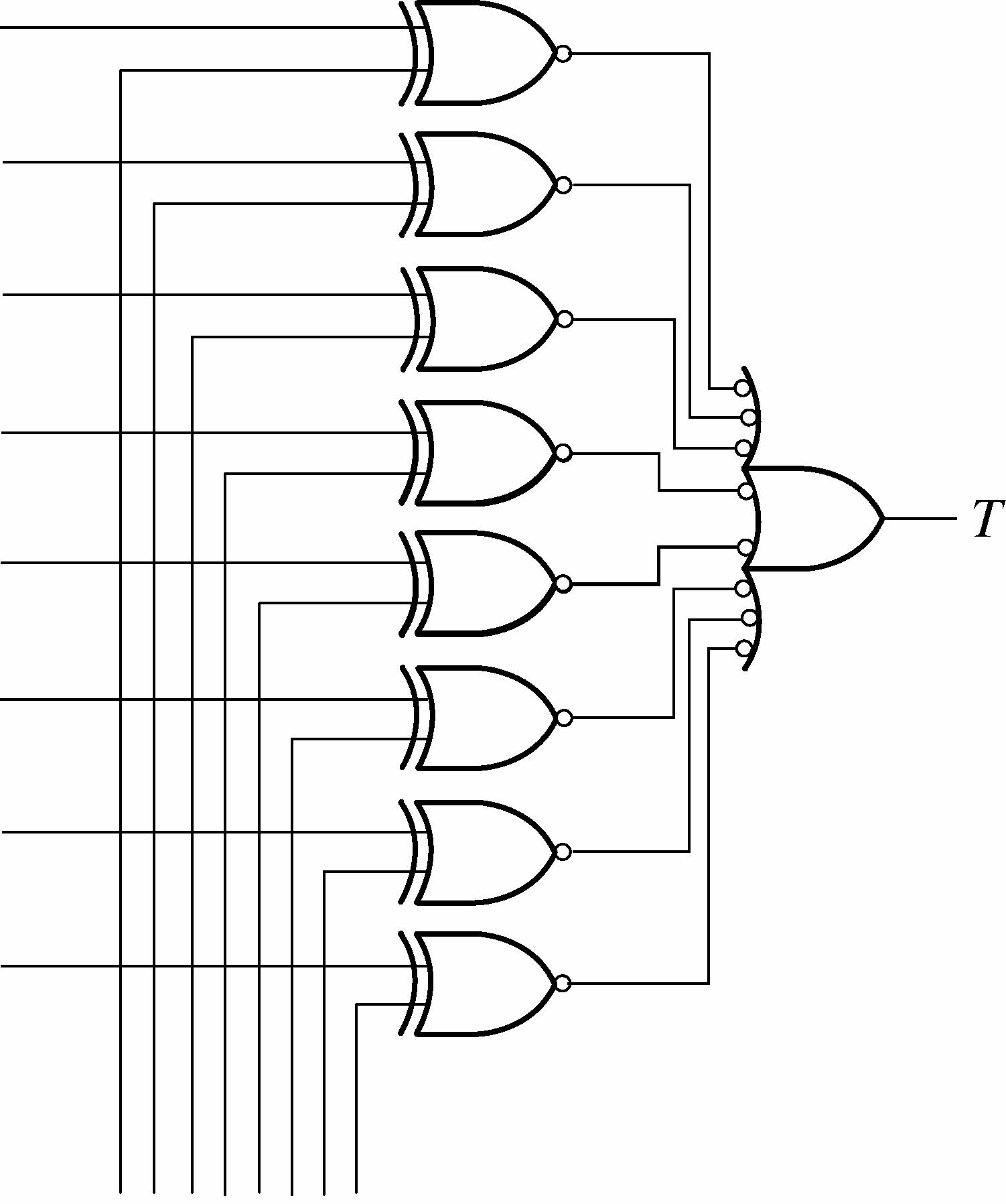
FIGURE 5-66
55. additiveminVTL = See Figure 5-67.
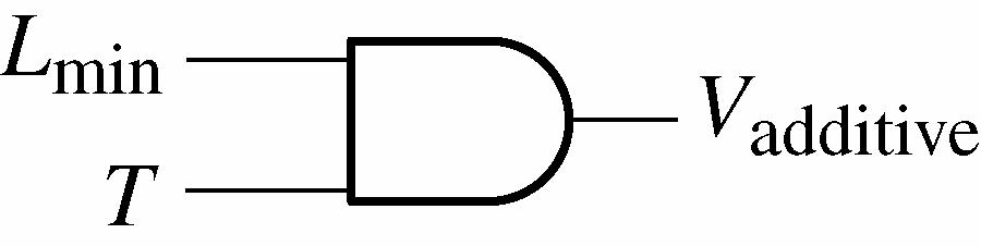
FIGURE 5-67
See Figure 5-68.
57. Let
X = Lamp on
A = Front door switch on
A = Front door switch off
B = Back door switch on
B = Back door switch off
X = AB B A + . This is an XOR operation.
See Figure 5-69.
5-69
58. See Figure 5-70.
5-70
59. Pin B of G1 open.
60. Pin C of OR gate open.
61. Inverter input open.
62. No fault.
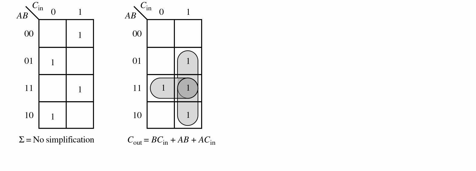
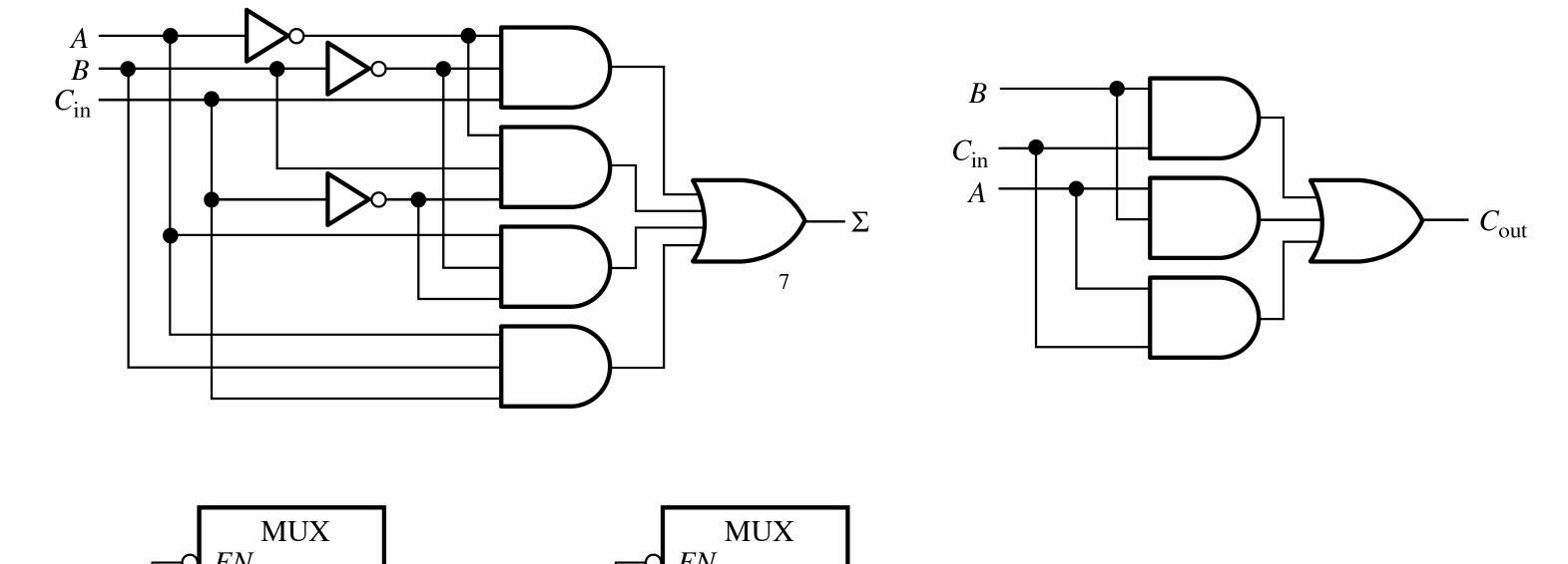
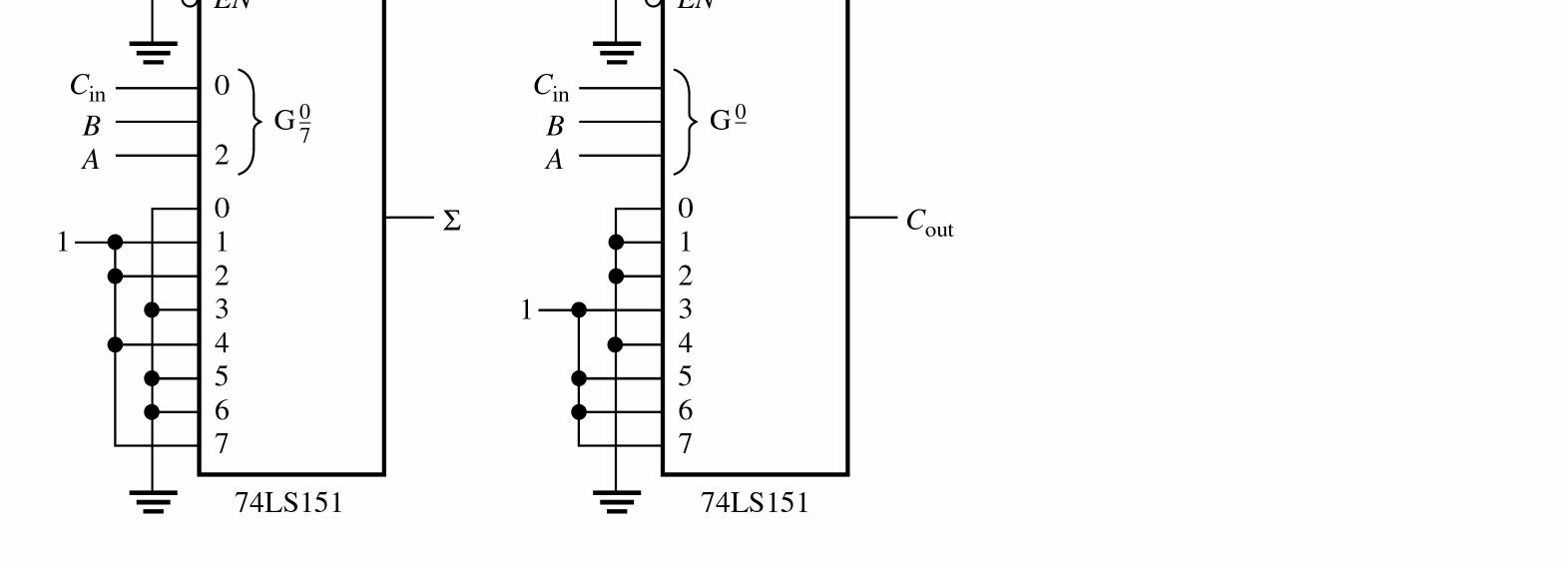
1. (a) XOR (upper) output = 0, Sum output = 1, AND (upper) output = 0, AND (lower) output = 1, Carry output = 1
(b) XOR (upper) output = 1, Sum output = 0, AND (upper) output = 1, AND (lower) output = 0, Carry output = 1
(c) XOR (upper) output = 1, Sum output = 1, AND (upper) output = 0, AND (lower) output = 0, Carry output = 0
2. (a) A = 0, B = 0, Cin = 0
(b) A = 1, B = 0, Cin = 0 or A = 0, B = 1, Cin = 0 or A = 0, B = 0, C in = 1
(c) A = 1, B = 1, Cin = 1
(d) A = 1, B = 1, Cin = 0 or A = 0, B = 1, Cin = 1 or A = 1, B = 0, Cin = 1
3. (a) Σ = 1, Cout = 0 (b) Σ = 1, Cout = 0 (c) Σ = 0, Cout = 1 (d) Σ = 1, Cout = 1
4. 111 See Figure 6-1. 101 1100
6-1
5. 10101 See Figure 6-2. 00111 11100
6. (a) When the / AddSubt is HIGH, the two numbers are subtracted.
(b) When the input is LOW, the numbers are added.
7. A = 1001 = 7, B = 1100 = 4
1001 0011 ← Complement of B 1 ← LSB Carry input 1101 = 3 in 2’s comp
8. See Figure 6-3.
Σ1 = 0110
Σ2 = 1011
Σ3 = 0110
Σ4 = 0001
Σ5 = 1000
10. 0100 1110 10010
Σ outputs should be Cout
4
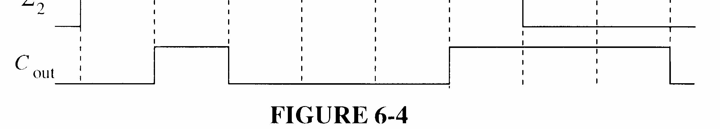
3Σ2Σ1 = 10010. The Σ3 output (pin 2) is HIGH and should be LOW.
See Figure 6-4.
6-4
11. tp(tot) = 40 ns + 6(25 ns) + 35 ns = 225 ns
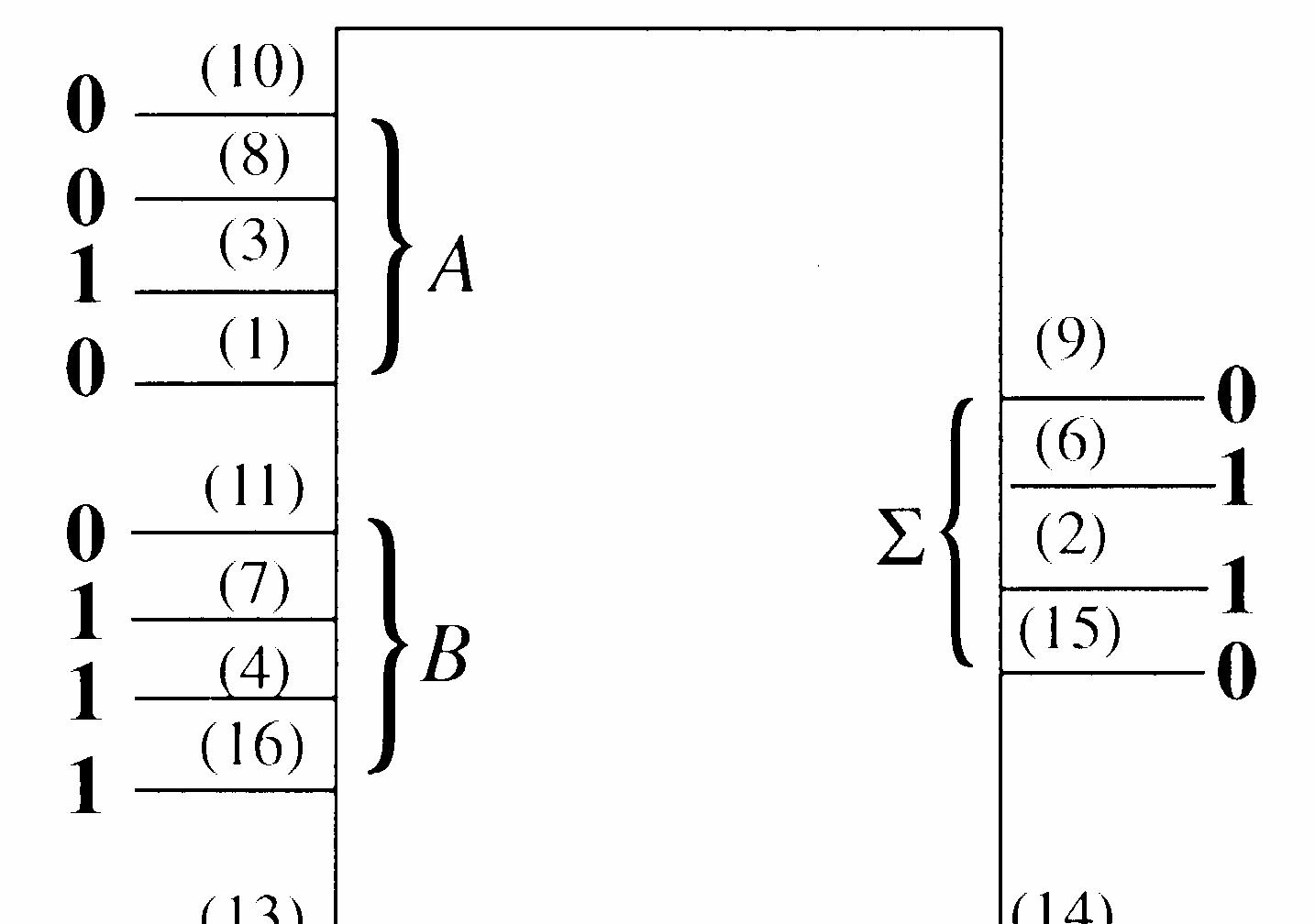
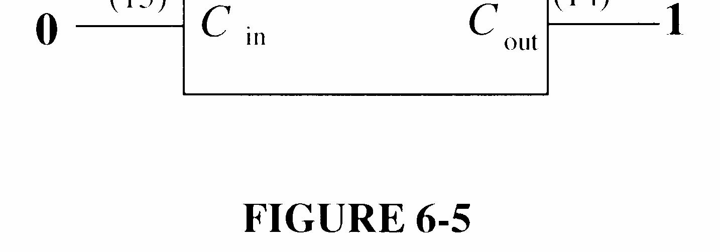
12. Full-adder 5:
Cin5 = Cout4 C
The logic to be added to text Figure 6-18 is shown in Figure 6-5.
6-5
13. The A = B output is HIGH when A0 = B0 and A1 = B1.
See Figure 6-6.
6-6
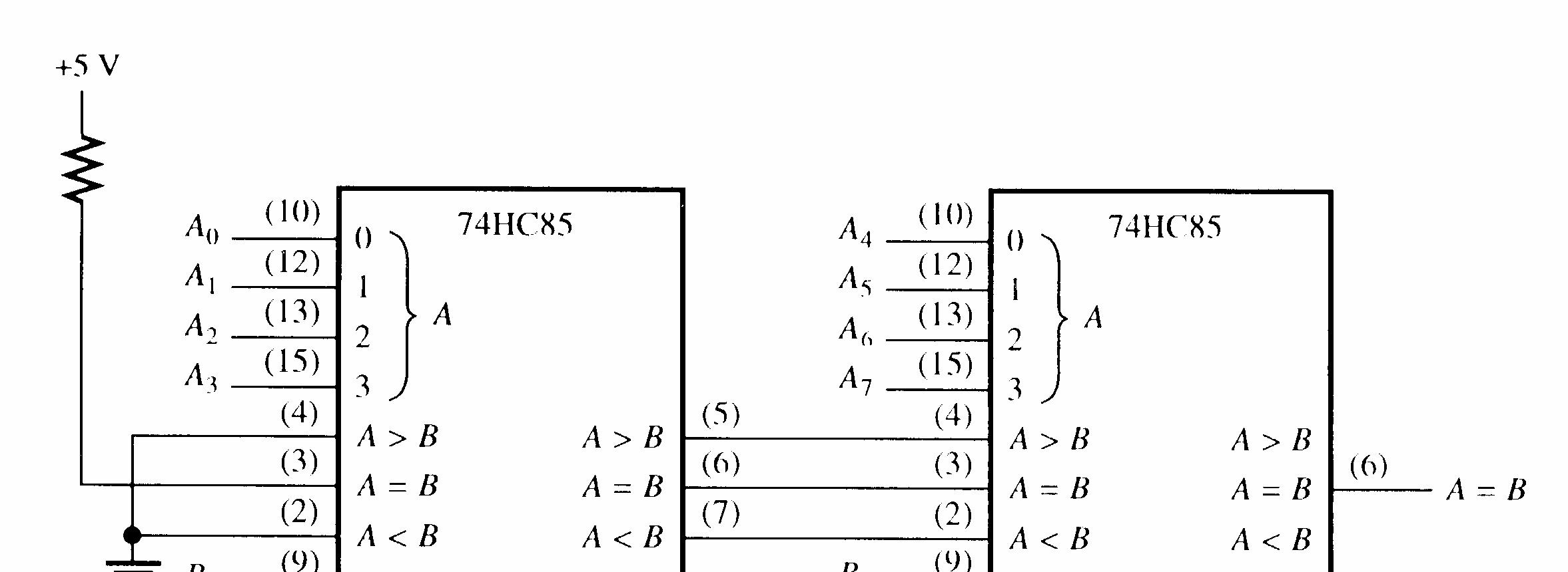
14. See Figure 6-7.
6-7
15. (a) A > B: 1, A = B: 0, A < B: 0 (b) A > B: 0, A = B: 0, A < B: 1 (c) A > B: 0, A = B: 1, A < B: 0
Section 6-5 Decoders
16. (a) A
(c)
17. See Figure 6-8.

18. Change the AND gates to NAND gates in Figure 6-8. 19. X =
See Figure 6-9.
20. Y =
See Figure 6-10.
6-10
21. See Figure 6-11.
6-11
22. 0 1 6 9 4 4 4 8 0
Section 6-6 Encoders
23. A0, A1, and A3 are HIGH. A3A2A1A0 = 1011, which is an invalid BCD code.
24. Pin 2 is for decimal 5, pin 5 is for decimal 8, and pin 12 is for decimal 2. The highest priority input is pin 5.
The completed outputs are: 0 1 2 3 A A A A = 0111, which is binary 8 (1000).
25. (a) 210 = 0010BCD = 00102
(b) 810 = 1000BCD = 10002
(c) 1310 = 00010011BCD = 11012
(d) 2610 = 00100110BCD = 110102
(e) 3310 = 00110011BCD = 1000012
26. (a) 1010101010 binary (b) 1111100000 binary 1111111111 gray 1000010000 gray
(c) 0000001110 binary (d) 1111111111 binary 0000001001 gray 1000000000 gray
See Figure 6-12.
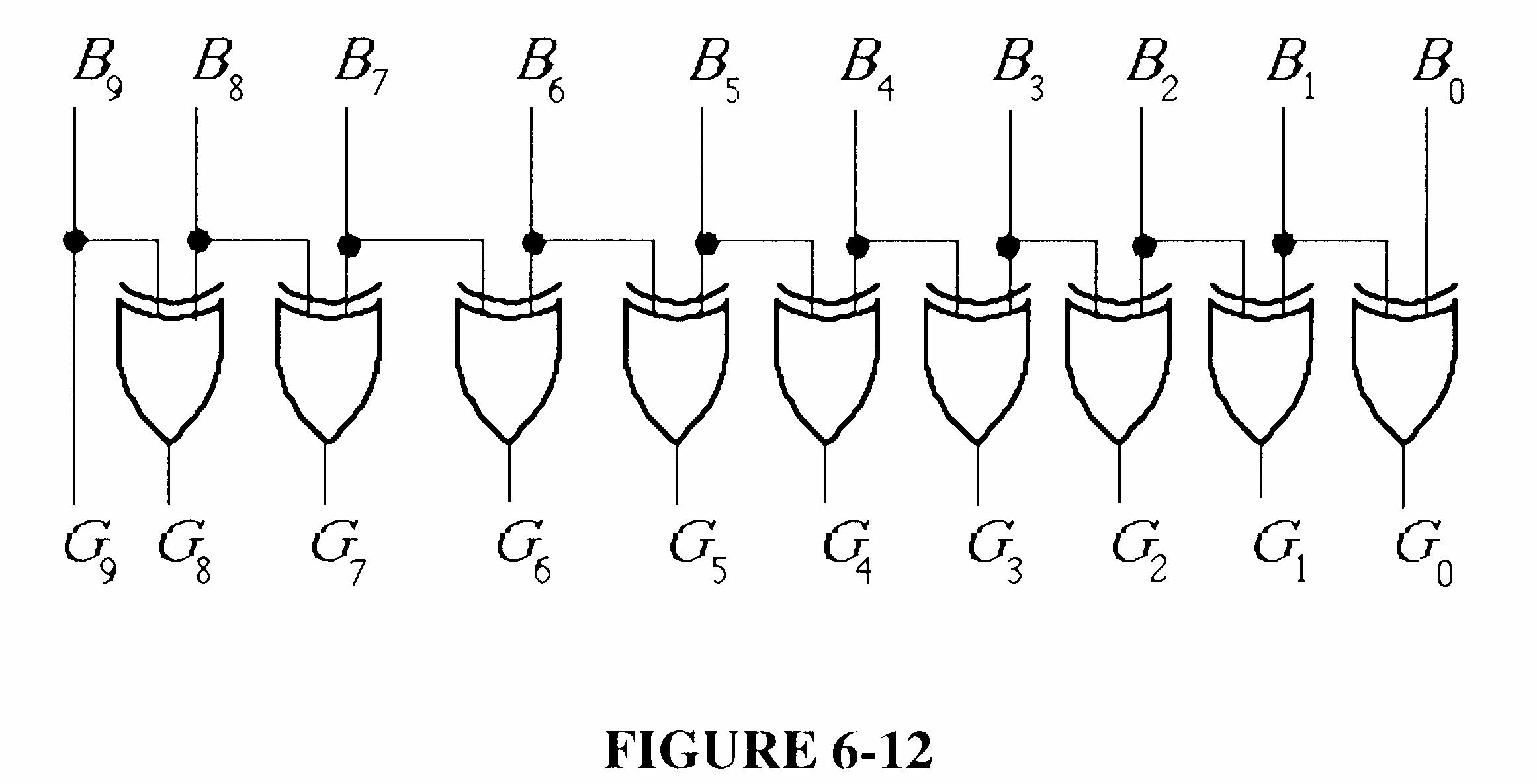
FIGURE 6-12
27. (a) 1010000000 gray (b) 0011001100 gray 1100000000 binary 0010001000 binary
(c) 1111000111 gray (d) 0000000001 gray 1010000101 binary 0000000001 binary
See Figure 6-13.
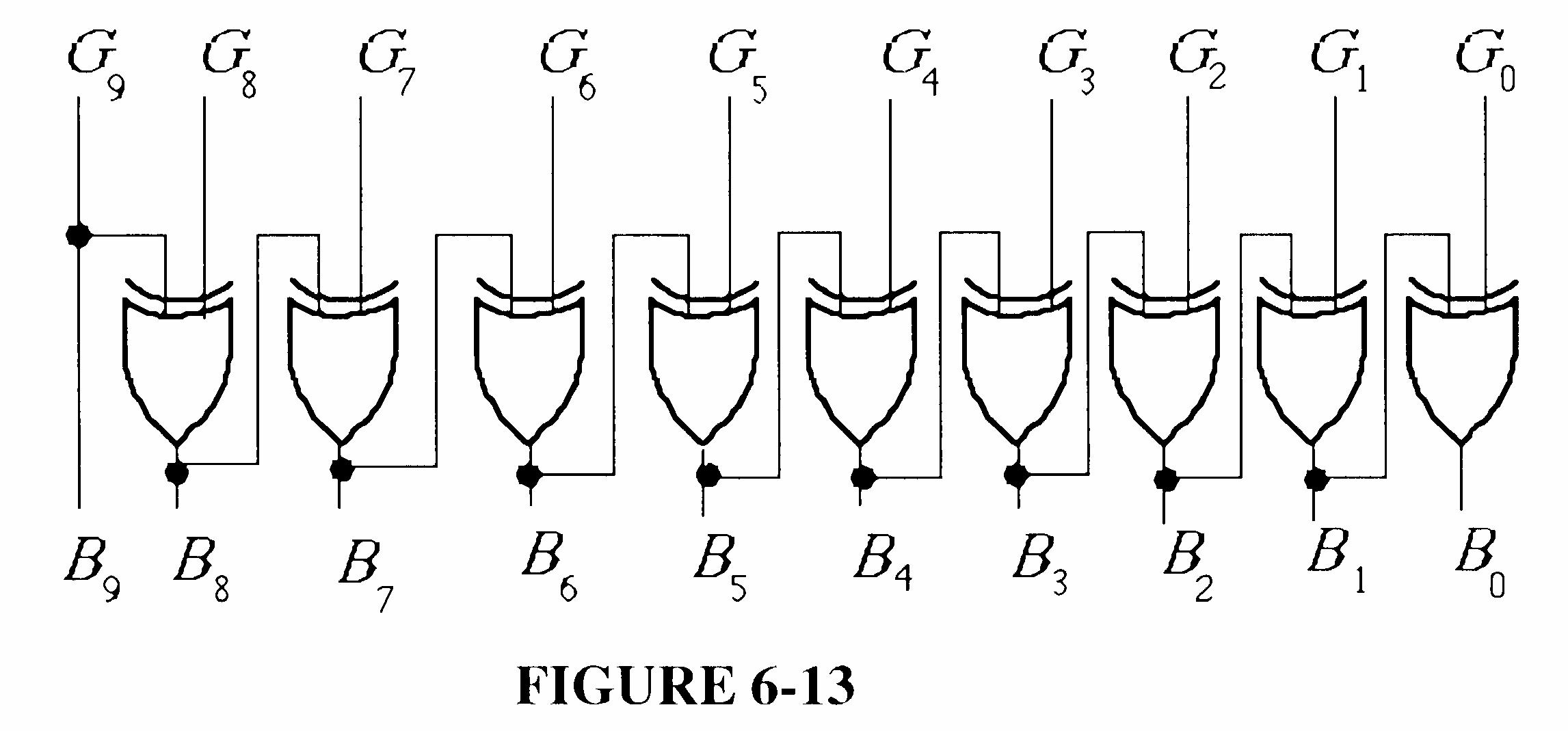
FIGURE 6-13
28. S1S0 = 01 selects, D1, therefore Y = 1.
29. See Figure 6-14.
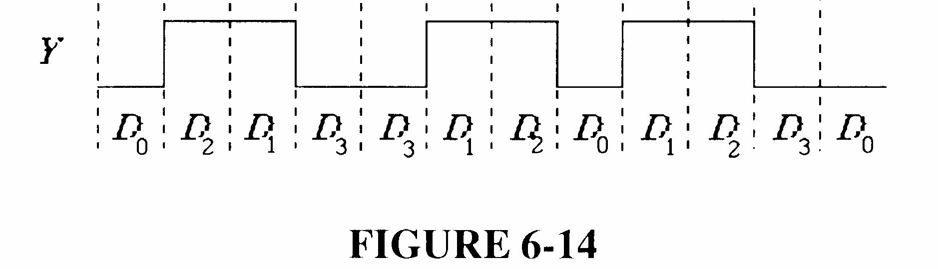
FIGURE 6-14
30. See Figure 6-15.
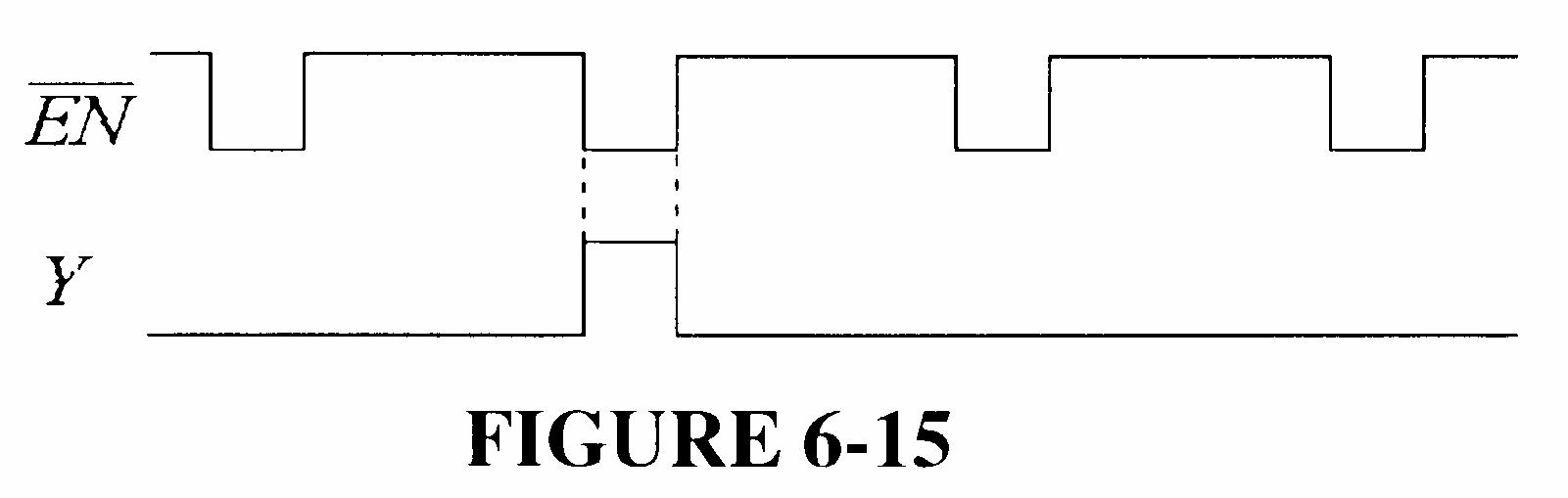
FIGURE 6-15
31. See Figure 6-16.
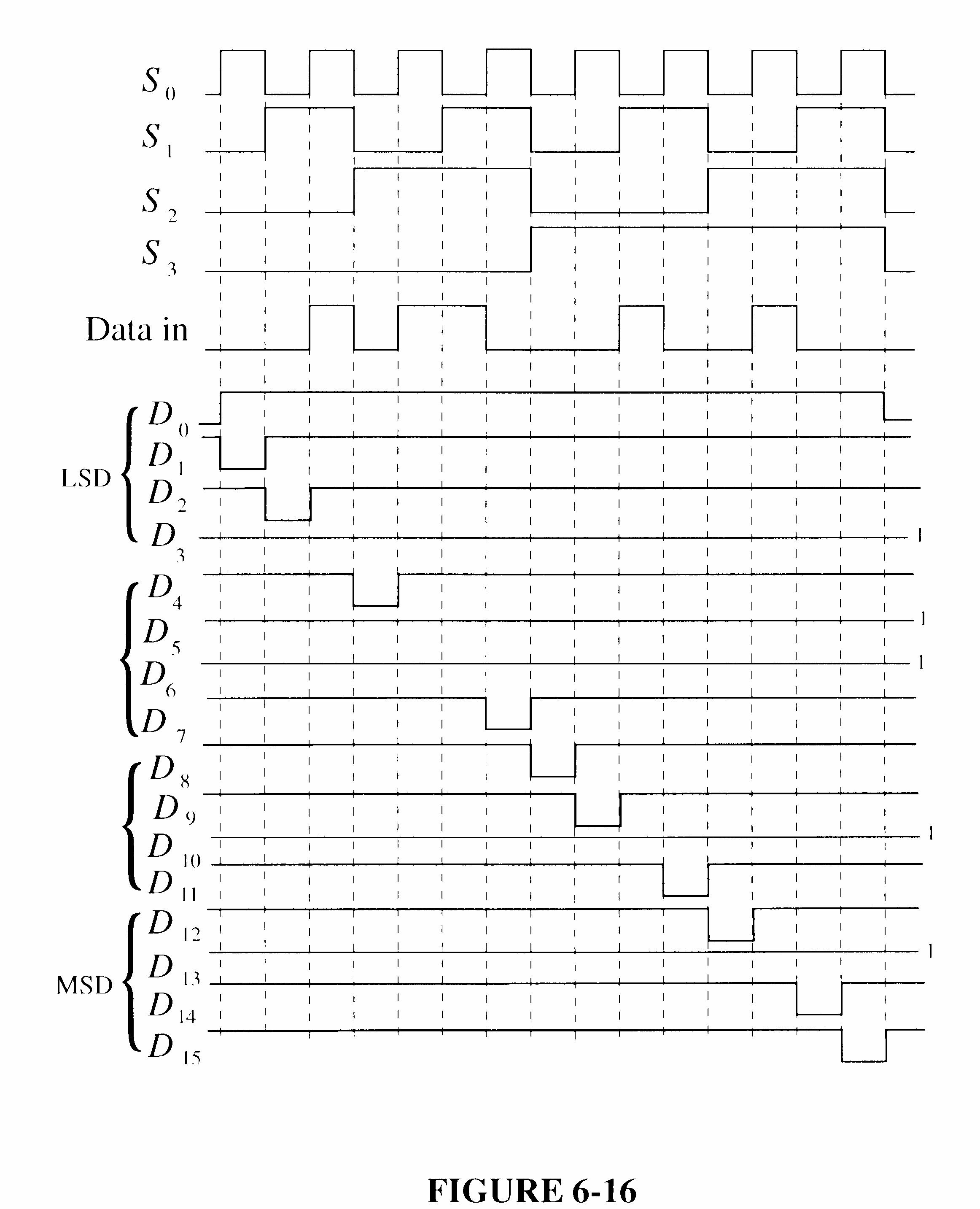
FIGURE 6-16
32. See Figure 6-17.
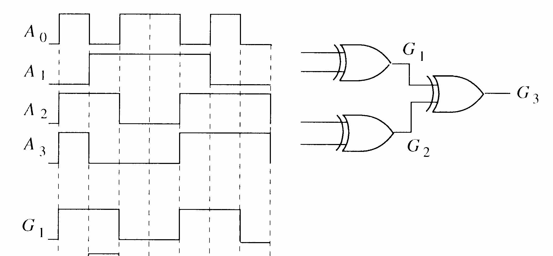
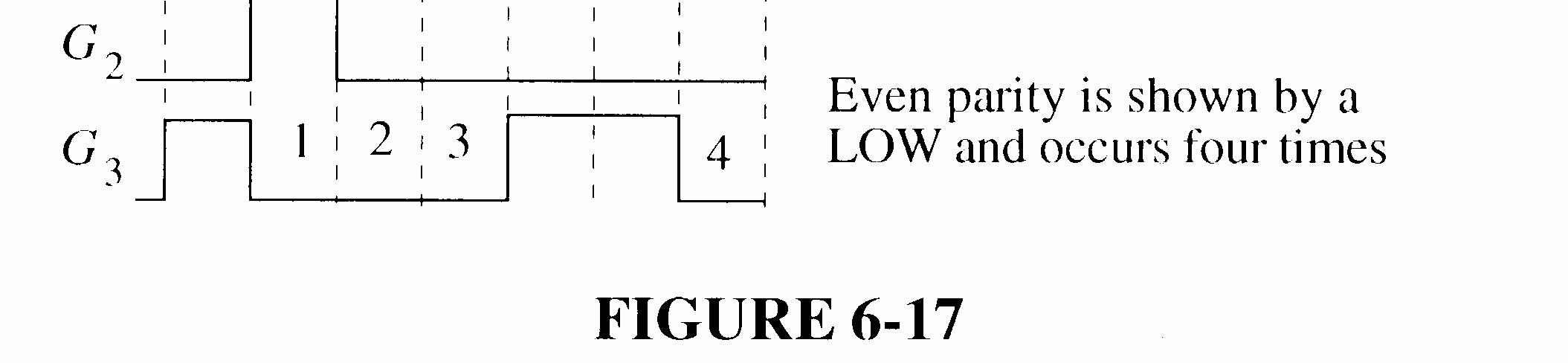
FIGURE 6-17
33. See Figure 6-18.
6-18
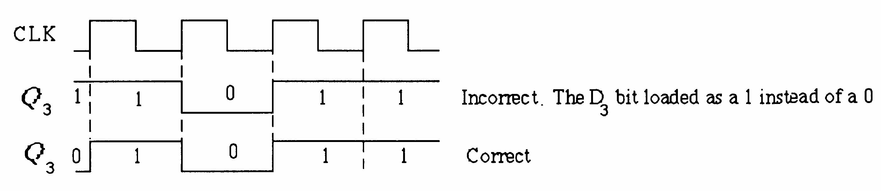
34. The outputs given in the problem are incorrect. By observation of these incorrect waveforms, we can conclude that the outputs of the device are not open or shorted because both waveforms are changing.
Observe that at the beginning of the timing diagram all inputs are 0 but the sum is 1. This indicates that an input is stuck HIGH. Start by assuming that Cin is stuck HIGH. This results in Σ and Cout output waveforms that match the waveforms given in the problem, indicating that Cin is indeed stuck HIGH, perhaps shorted to VCC
See Figure 6-19 for the correct output waveforms.
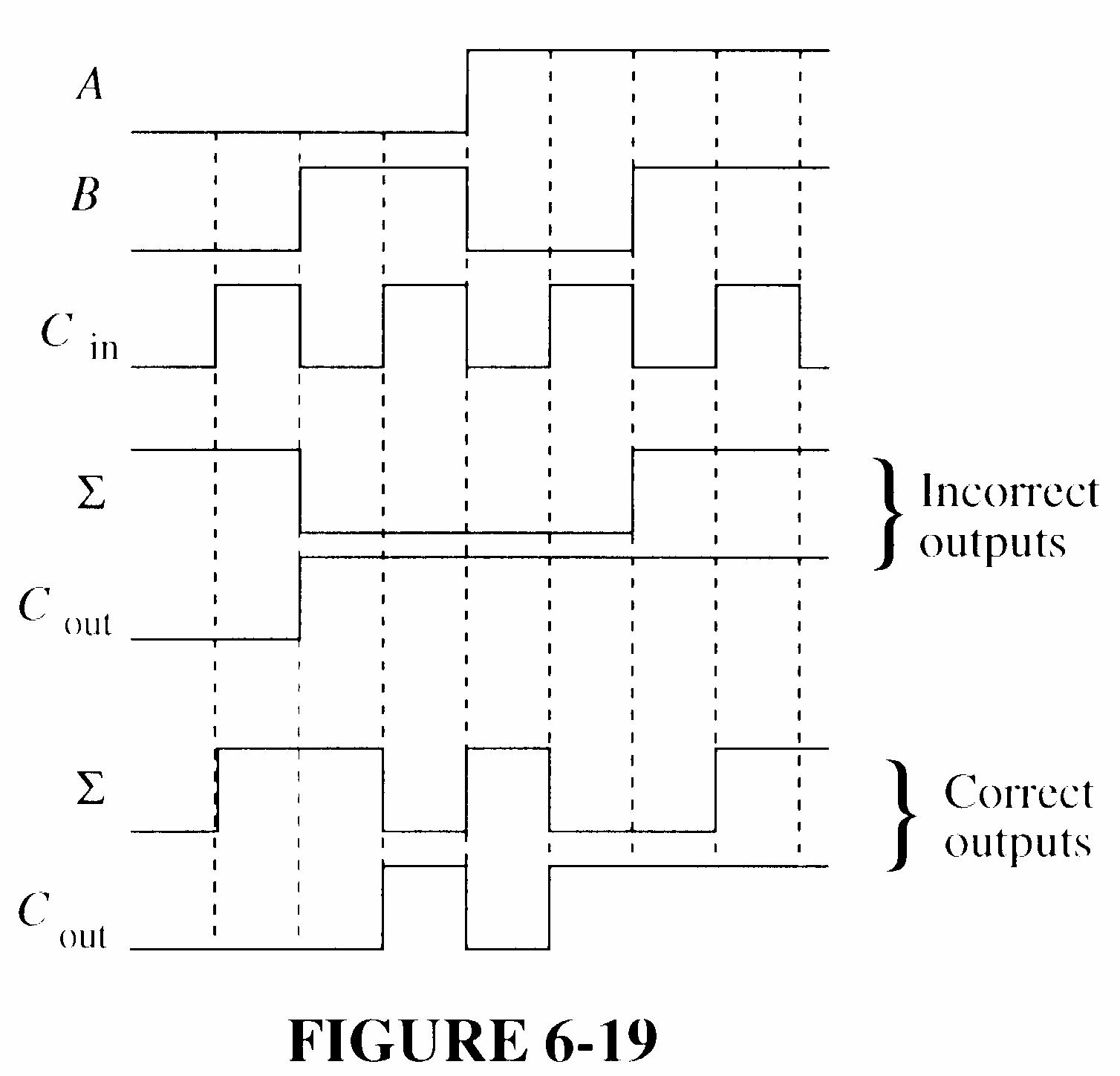
FIGURE 6-19
35. (a) OK (b) Segment g burned out; output G open (c) Segment b output stuck LOW
36. Step 1: Verify that the supply voltage is applied.
Step 2: Go through the key sequence and verify the output code in Table 1.
TABLE 1
Step 3: Check for proper priority operation by repeating the key sequence in Table 1 except that for each key closure, hold that key down and depress each lower-valued key as specified in Table 2.
Hold down keys Depress keys one at a time A
1 2 3 4 5 6 7 8 9 0 1, 0 2, 1, 0 3, 2, 1, 0 4, 3, 2, 1, 0 5, 4, 3, 2, 1, 0 6, 5, 4, 3, 2, 1, 0 7, 6, 5, 4, 3, 2, 1, 0 8, 7, 6, 5, 4, 3, 2, 1, 0
TABLE 2
37. (a) Open A1 input acts as a HIGH. All binary values corresponding to a BCD number having a 1’s value of 0, 1, 4, 5, 8, or 9 will be off by 2. This will first be seen for a BCD value of 00000000.
(b) Open Cout of top adder. All values not normally involving a carry out will be off by 32. This will first be seen for a BCD value of 00000000.
(c) The Σ4 output of top adder is shorted to ground. Same binary values above 15 will be short by 16. The first BCD value to indicate this will be 00011000.
(d) Σ3 of bottom adder is shorted to ground. Every other set of 16 value starting with 16 will be short 16. The first BCD value to indicate this will be 00010110.
38. (a) The 1Y1 output of the 74LS139 is stuck HIGH or open; B cathode open.
(b) No power; EN input to the 74LS139 is open
(c) The f output of the 74LS47 is stuck HIGH
(d) The frequency of the data select input is too low
39. 1. Place a LOW on pin 7 (Enable).
2. Apply a HIGH to D0 and a LOW to D1 through D7
3. Go through the binary sequence on the select inputs and check Y and Y according to Table 3.
TABLE 3
4. Repeat the binary sequence of select inputs for each set of data inputs listed in Table 4. A HIGH on the Y output should occur only for the corresponding combinations of select inputs shown.
TABLE 4
40. The Σ EVEN output of the 74LS280 should be HIGH and the output of the error gate should be HIGH because of the error condition. Possible faults are:
1. Σ EVEN output of the 74LS280 stuck LOW
2. Error gate faulty.
3. The ODD input to the 74LS280 is open thus acting as a HIGH.
4. The inverter going to the ODD input of the 74LS280 has an open output or the output is stuck HIGH
41. Apply a HIGH in turn to each Data input, D0 through D7 with LOWs on all the other inputs. For each HIGH applied to a data input, sequence through all eight binary combinations of select inputs (S2S1S0) and check for a HIGH on the corresponding data output and LOWs on all the other data outputs.
One possible approach to implementation is to decode the S2S1S0 inputs and generate an inhibit pulse during any given bit time as determined by the settings of seven switches. The inhibit pulse effectively changes a LOW on the Y serial data line to a HIGH during the selected bit time(s), thus producing a bit error. A basic diagram of this approach is shown in Figure 6-20.

System Application Activity
42. See Figure 6-21.
43. See Figure 6-22.
6-22
44. See Figure 6-23.
See Figure 6-24.
See Figure 6-25.

6-25
47. See Figure 6-26.

6-26
48. See Figure 6-27.
49. See Figure 6-28.
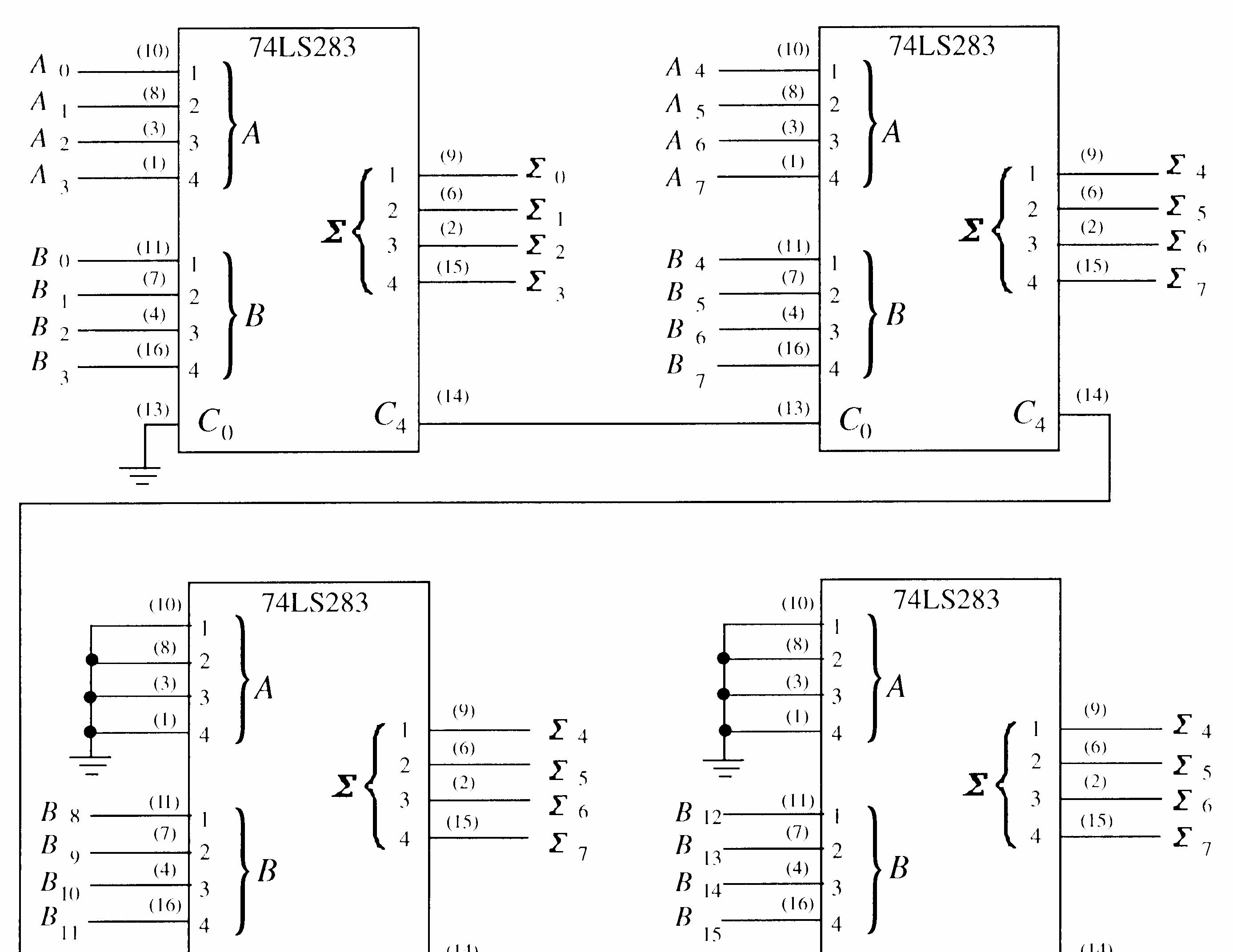
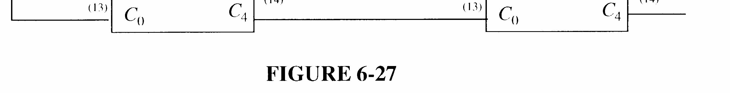
50. See Figure 6-29.
51. See Figure 6-30.

52. See Figure 6-31.
6-31
53. LSB adder carry output open.
54. Pins 4 and 5 shorted together.
55. Pin 12 of upper 74148 open.
56. Pin 3 of upper 74151 open.
Section 7-1 Latches
1. See Figure 7-1.
2. See Figure 7-2.
3. See Figure 7-3.
4. See Figure 7-4.
5. See Figure 7-5.
6. See Figure 7-6.
7. See Figure 7-7.
7-7
8. See Figure 7-8.
7-8
9. See Figure 7-9.
7-9
10. See Figure 7-10.
11. See Figure 7-11.
12. See Figure 7-12.

13. See Figure 7-13.
14. See Figure 7-14.
7-14
15. See Figure 7-15.
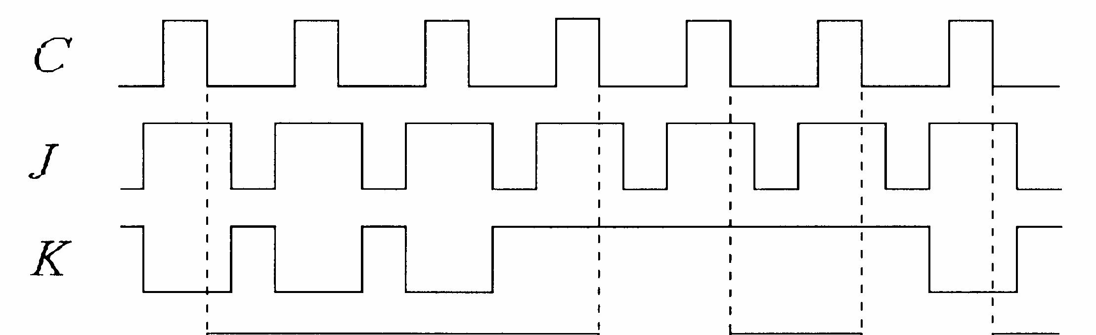
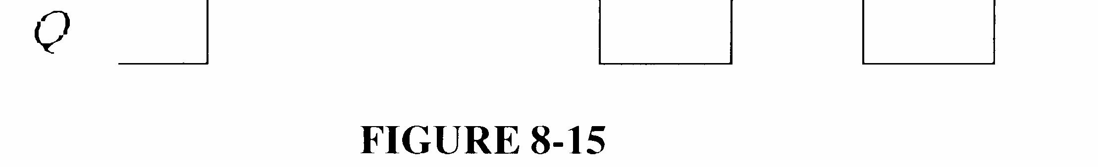
FIGURE 7-15
16. J: 0010000
K: 0000100
Q: 0011000
17. See Figure 7-16.
7-16
18. See Figure 7-17.
7-17
19. The direct current and dc supply voltage
20. tPLH (Clock to Q):
Time from triggering edge of clock to the LOW-to-HIGH transition of the Q output.
tPHL (Clock to Q):
Time from triggering edge of clock to the HIGH-to-LOW transition of the Q output.
tPLH PRE ( to Q):
Time from assertion of the Preset input to the LOW-to-HIGH transition of the Q output.
tPHL (CLR to Q):
Time from assertion of the clear input to the HIGH-to-LOW transition of the Q output.
21. Tmin = 30 ns + 37 ns = 67 ns
fmax = Tmin 1 = 14.9 MHz
22. See Figure 7-18.
7-19
23. IT = 15(10 mA) = 150 mA PT = (5 V)(150 mA) = 750 mW
24. See Figure 7-19.
Section 7-4 Flip-Flop Applications
25. See Figure 7-20.
26. See Figure 7-21.
Section 7-5 One-Shots
27. tW = 0.7RCEXT = 0.7(3.3 kΩ)(2000 pF) = 4.62 μs
=
29. See Figure 7-22.
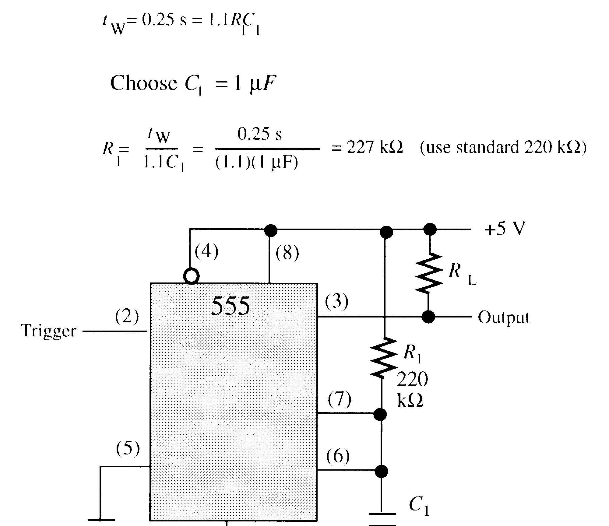
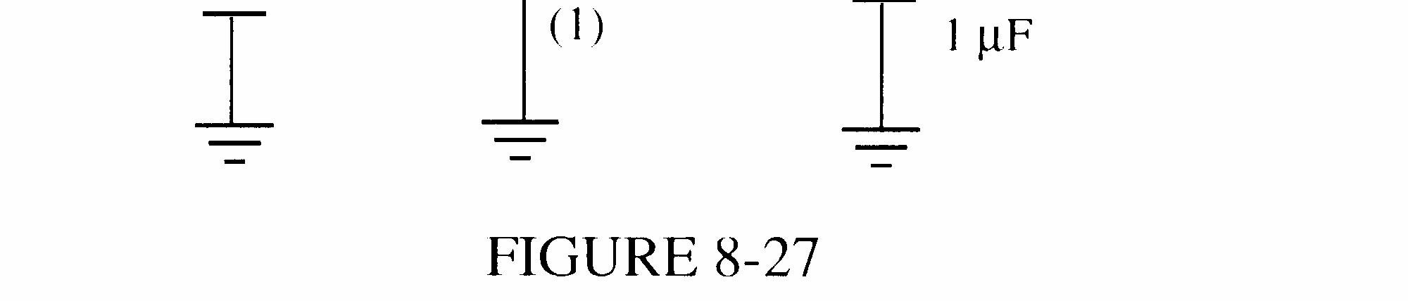
FIGURE 7-22
Section 7-6 Astable Multivibrator
30. f = 122 11 0.7(2)0.7(10002200)(0.01F) RRC = +Ω+Ωμ = 44.6 kHz
31. T = kHz 20 1 1 = f = 50 μs For a duty cycle of 75%: tH = 37.5 μs and tL = 12.5 μs
R1 + R2 = F) 0.7(0.002 s 37.5 0.7 μ μ = C t H = 26,786 Ω
R2 = F) 0.7(0.002 s 12.5 7 0 μ μ = C t L = 8,929 Ω (use 9.1 kΩ)
R1 = 26,786 Ω R2 = 26,786 Ω 8,929 Ω = 17,857 Ω (use 18 kΩ)
32. The flip-flop in Figure 7-94 of the text has an internally open J input.
33. The wire from pin 6 to pin 10 and the ground wire are reversed. Pin 7 should be at ground and pin 6 connected to pin 10.
34. See Figure 7-23.
35. Since none of the flip-flops change, the problem must be a fault that affects all of them. The two functions common to all the flip-flops are the clock (CLK) and clear ) (CLR inputs. One of these lines must be shorted to ground because a LOW on either one will prevent the flipflops from changing state. Most likely, the CLR line is shorted to ground because if the clock line were shorted chances are that all of the flip-flops would not have ended up reset when the power was turned on unless an initial LOW was applied to the CLR at power on.
36. Small differences in the switching times of flip-flop A and flip-flop B due to propagation delay cause the glitches as shown in the expanded timing diagram in Figure 7-24. The delays are exaggerated greatly for purposes of illustration. Glitches are eliminated by strobing the output with the clock pulse.
37. (a) See Figure 7-25.
(b) KB open acts as a HIGH and the operation is normal. The timing diagram is the same as Figure 7-25.
(c) See Figure 7-26.
7-26
(d) X remains LOW if QB = 1 0) ( = QB . X follows QA if QB = 0 1) ( = QB .
(e) See Figure 7-27.
7-27
38. tW = 0.7RCEXT
One-shot A: tW = 0.7(0.22 μF)(100 kΩ) = 15.4 ms
One-shot B: tW = 0.7(0.1 μF)(100 kΩ) = 7 ms
The pulse width of one shot A is apparently not controlled by the external components and the one-shot is producing its minimum pulse width of about 40 ns. An open pin 11 would cause this problem. See Figure 7-28.
7-28
39. For the 6 s timer let C1 = 1 μF
R1 = 6 s (1.1)(1 F)μ = 5.5 MΩ (use 5.6 MΩ)
For the 40 s timer let C1 = 2.2 μF
R1 = 40 s (1.1)(2.2 F)μ = 16.5 MΩ (use 15 MΩ)
See Figure 7-29.
6 s timer and 40 s timer are the same except for the component values calculated above.
FIGURE 7-29
40. tW = 6 s. Let CEXT = 1 μF.
tW = 0.7
μ
tW = 40 s. Let CEXT = 10 μF.
See Figure 7-30.
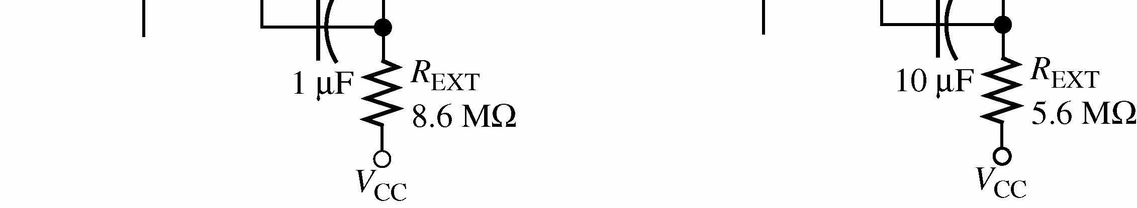
FIGURE 7-30
41. tW = 6 s. Let C
See Figure 7-31.
42. See Figure 7-32.
43. See Figure 7-33 for one possibility.
44. Changes required for the system to incorporate a 15 s left turn signal on main:
1. Change the 2-bit gray code sequence to a 3-bit sequence.
2. Add decoding logic to the State Decoder to decode the turn signal state.
3. Change the Output Logic to incorporate the turn signal output.
4. Change the Trigger Logic to incorporate a trigger output for the turn signal timer.
5. Add a 15 second timer.
See Figure 7-34.

45. Q output of U1 open.
46. K input of U2 open.
47. SET input of U1 open.
48. No fault.
49. K input of U2 open.
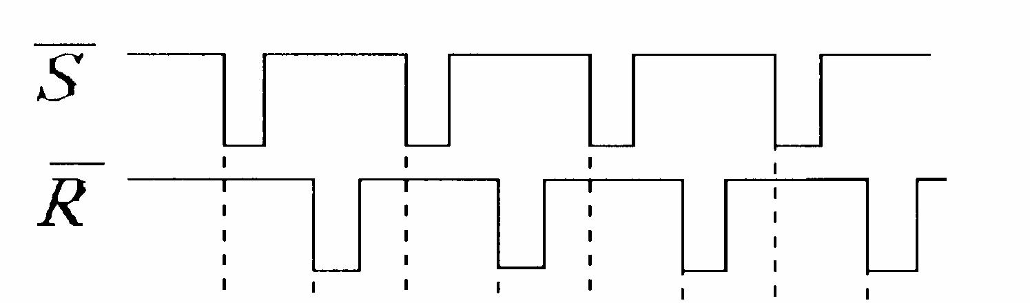
1. See Figure 8-1.
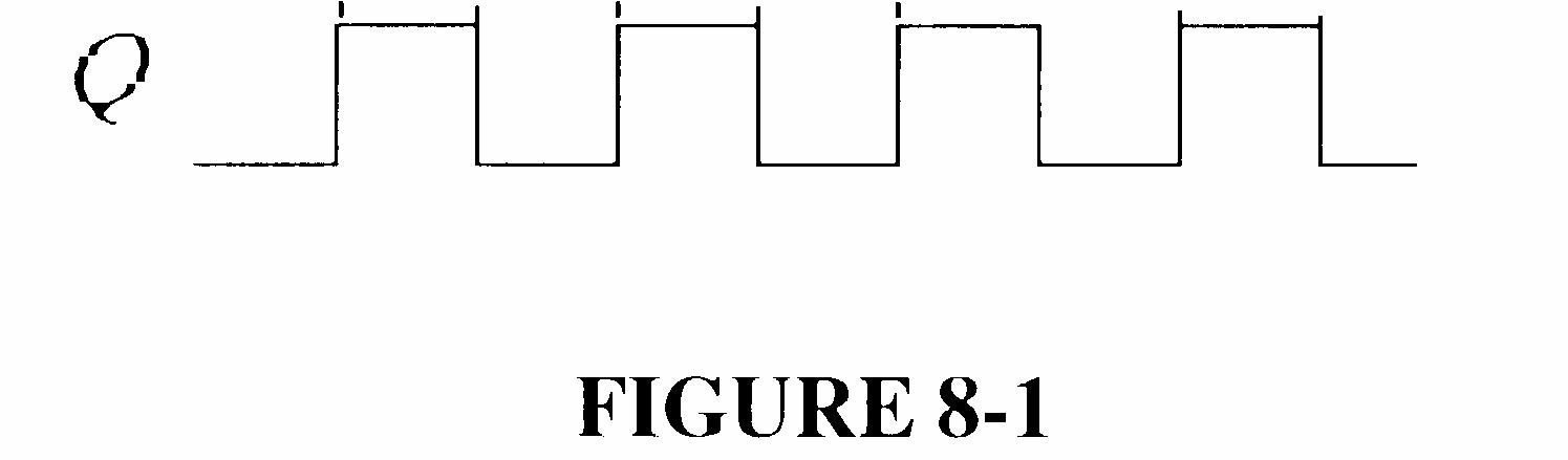
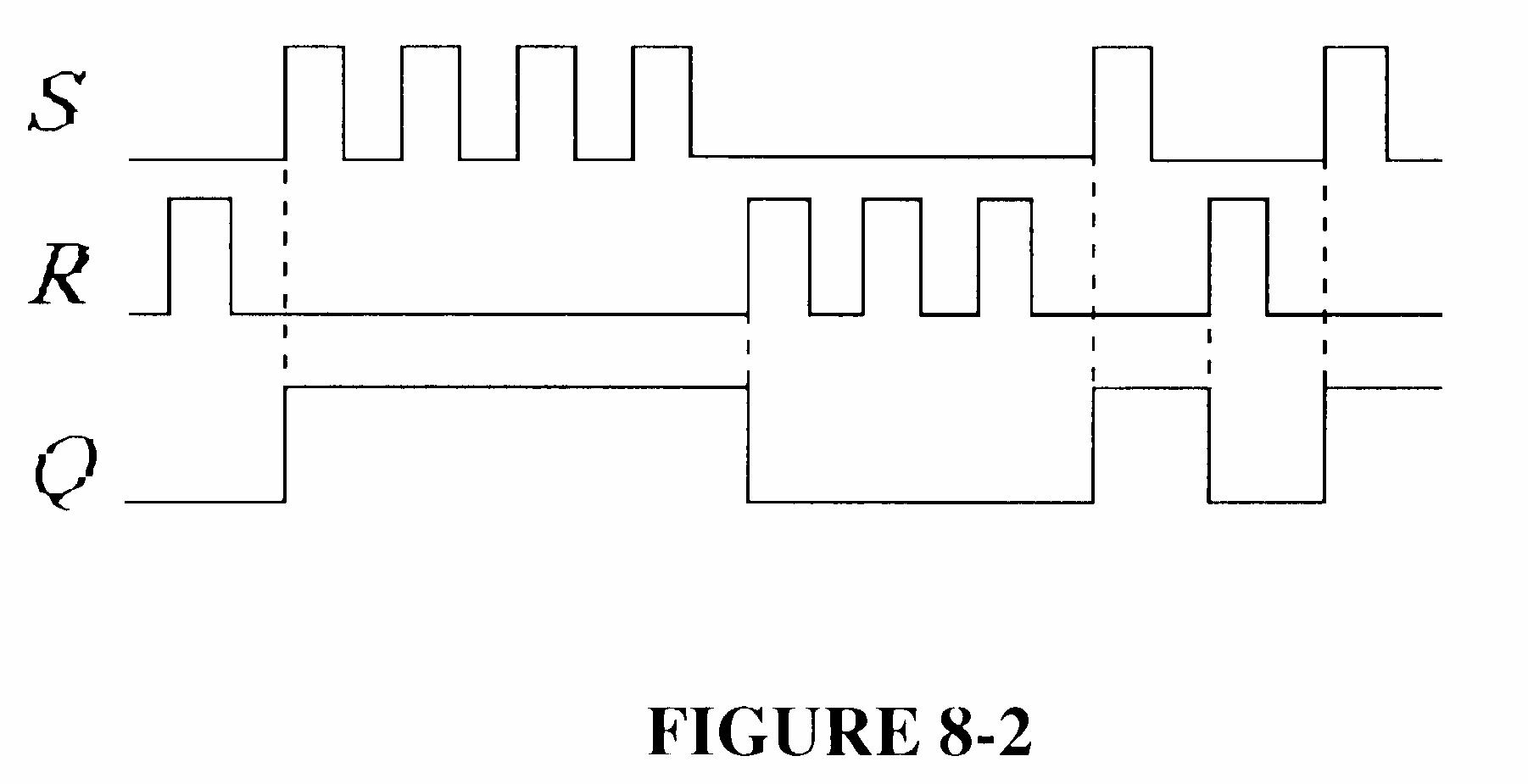
2. See Figure 8-2.
3. tp(max) = 3(8 ns) = 24 ns
Worst-case delay occurs when all flip-flops change state from 011 to 100 or from 111 to 000.
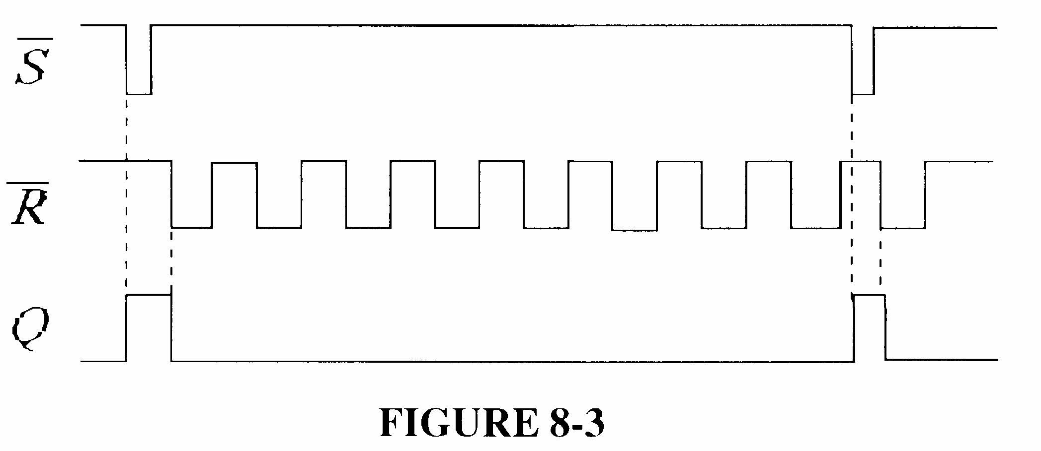
4. See Figure 8-3.
8-3
5. 8 ns, the time it takes one flip-flop to change state.
6. See Figure 8-4.
8-4
7. Each flip-flop is initially reset.
8. See Figure 8-5.
8-5
9. See Figure 8-6.
8-6
10. See Figure 8-7.
8-7
11. See Figure 8-8.
12. See Figure 8-9.
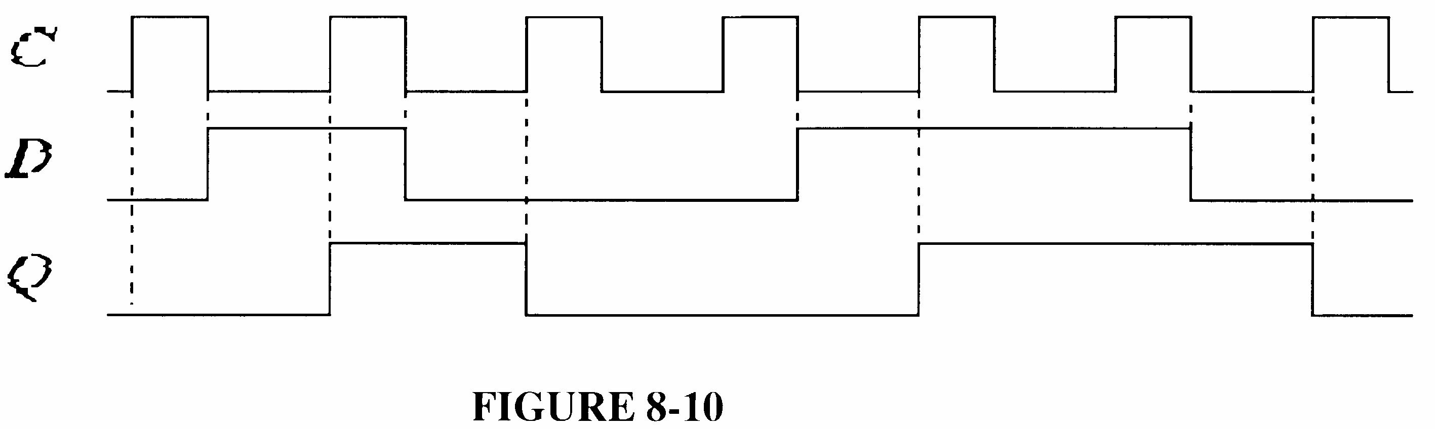
13. See Figure 8-10.
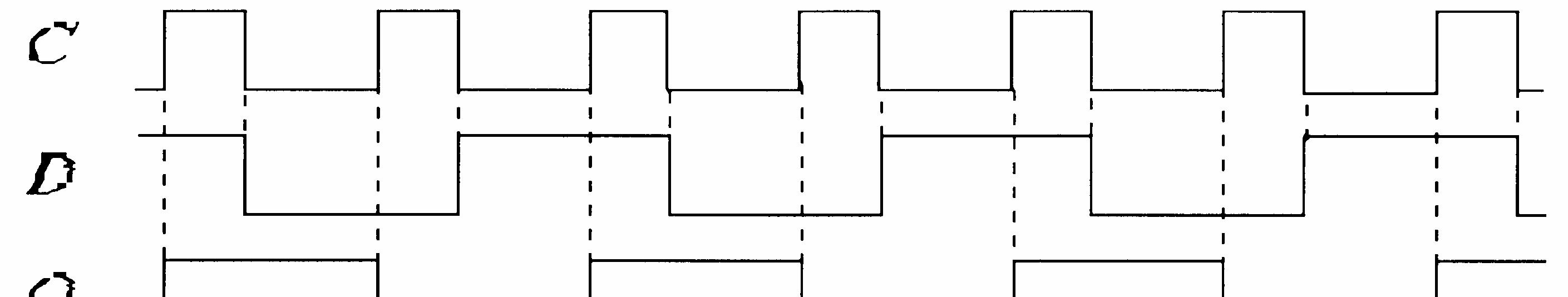
14. See Figure 8-11.
8-9
8-10
8-11
15. See Figure 8-12.
(NOTE: The text answer, Figure P-64, is incorrect in the first printing. It will be corrected to match Figure 8-12 in the 2nd printing.)
16.
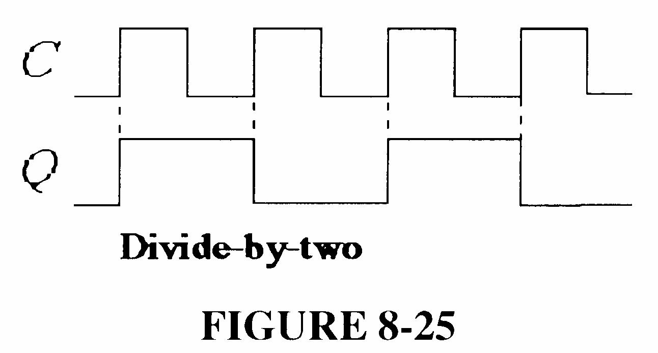
The sequence is 000 to 001 to 011 to 111 to 110 to 100 and back to 001, etc.
Initially
After CLK 1
After CLK 2
After CLK 3
After CLK 4
After CLK 5
Tog = toggle, NC = no change
The counter locks up in the 1010 and 0101 states, alternating between them.
18. NEXT-STATE TABLE
Present State Next State
TRANSITION TABLE
Output State Transitions (Present state to next state)
See Figure 8-13.
Flip-Flop Inputs
19. NEXT-STATE TABLE
TRANSITION TABLE Output
8-13
See Figure 8-14.
Output State Transition (Present State to next state)
to 1
to 0
to 1 1 to 0
to 0
to 0 0 to 0 0 to 0 0 to 0 0 to 0
to 0
Flip-flop Inputs
Binary states for 10, 11, 12, 13, 14, and 15 are unallowed and can be represented by don’t cares.
See Figure 8-15. Counter implementation is straightforward from input expressions.
FIGURE 8-15
21. NEXT-STATE TABLE
TRANSITION TABLE
0 to 1 0 to 0
0 to 0 0 to 0 0 to 0 0 to 0 0 to 0 0 to 1 1 to 0 1 to 1 1 to 1 1 to 0 0 to 0 0 to 0 0 to 0 0 to 1 1 to 0 1 to 1 1 to 1 1 to 0
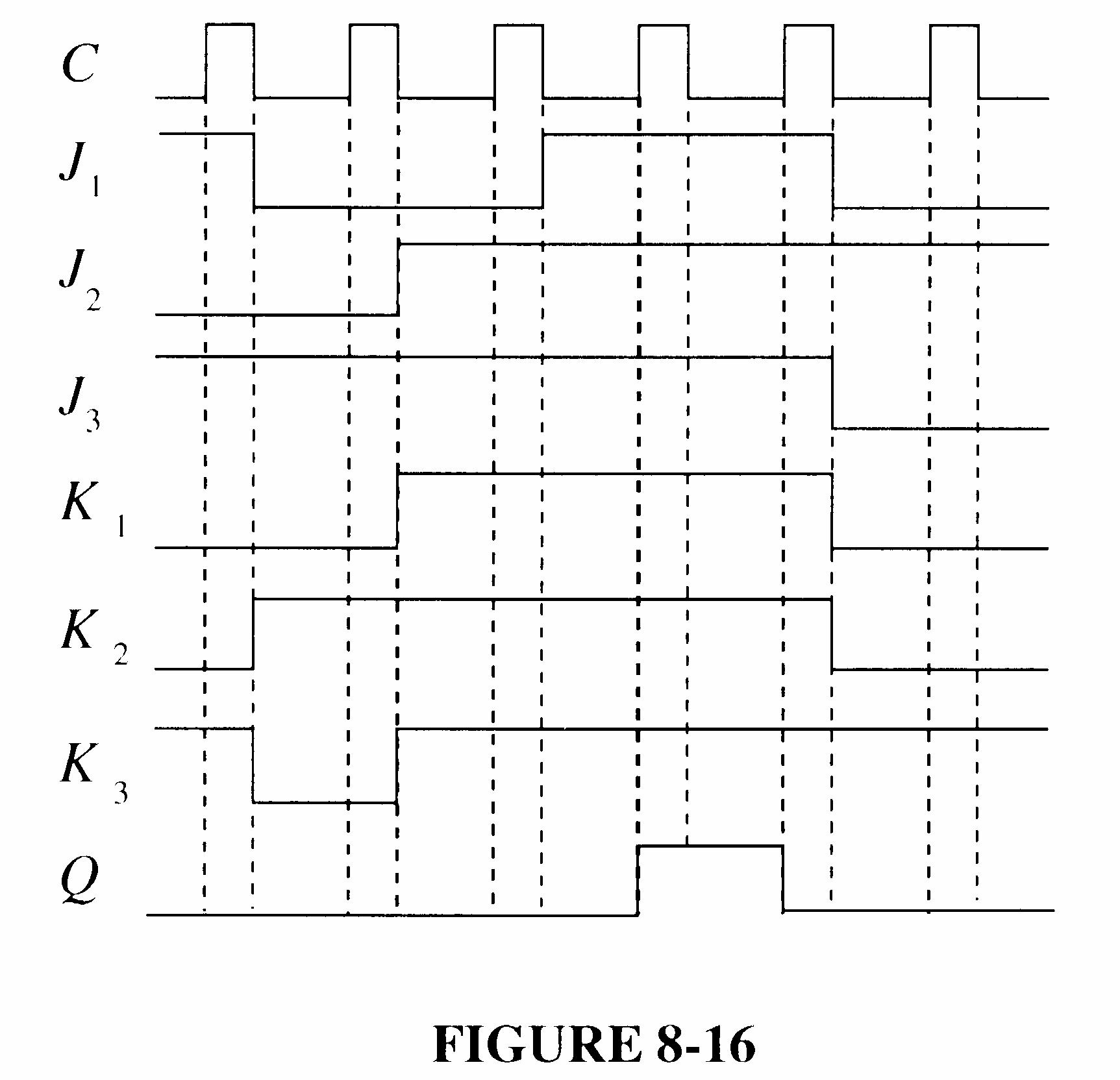
See Figure 8-16.
X0 X1
Section 8-5 Cascaded Counters
22. (a) Modulus = 4 × 8 × 2 = 64 f1 = 4 kHz
8-16
(b) Modulus = 10 × 10 × 10 × 2 = 2000
f1 = 10 kHz 100 = 10 kHz
f2 = 10 kHz 10 = 1 kHz
f3 = 10 kHz 1 = 100 Hz
f4 = 2 Hz 100 = 50 Hz
(c) Modulus = 3 × 6 × 8 × 10 × 10 = 14400
f1 = 3 MHz 21 = 7 MHz
f2 = 6 MHz 7 = 1.167 MHz
f3 = 8 MHz 167 1 = 145.875 kHz
f4 = 10 kHz 145.875 = 14.588 kHz
f5 = 10 kHz 588 14 = 1.459 kHz
(d) Modulus = 2 × 4 × 6 × 8 × 16 = 6144
f1 = 2 kHz 39.4 = 19.7 kHz
f2 = 4 kHz 19.7 = 4.925 kHz
f3 = 6 kHz 925 4 = 820.83 Hz
f4 = 8 820.683 = 102.6 Hz
f5 = 16 Hz 6 102 = 6.41 Hz
23. See Figure 8-17.
FIGURE 8-17
24. See Figure 8-18.
25. See Figure 8-19.
26. See Figure 8-20.
8-19
8-20
27. The states with an asterisk are the transition states that produce glitches on the decoder outputs. The glitches are indicated on the waveforms in Figure 8-20 (Problem 8-26) by short vertical lines.
Initial 0000
CLK 1 0001
CLK 2 0000 * 0010
CLK 3 0011
CLK 4 0010 * 0000 * 0100
CLK 5 0100
CLK 6 0100 * 0110
CLK 7 0111
CLK 8 0110 * 0100 * 0000 * 1000
CLK 9 1001
CLK 10 1000* 1010
CLK 11 1011
CLK 12 1010 * 1000 * 1100
CLK 13 1101
CLK 14 1100 * 1110
CLK 15 1111
CLK 16 1110 * 1100 * 1000 * 0000
28. See Figure 8-21.
8-21
29. See Figure 8-22.
8-22
30. 1 There is a possibility of a glitch on decode 2 at the positive-going edge of CLK 4 if the propagation delay of FF0 is less than FF1 or FF2.
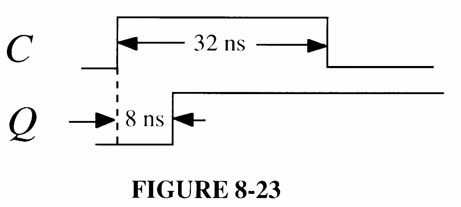
2 There is a possibility of a glitch on decode 7 at the positive-going edge of CLK 4 if the propagation delay of FF2 is less than FF0 and FF1.
3 There is a possibility of a glitch on decode 7 at the positive-going edge of CLK 6 if the propagation delay of FF1 is less than FF0.
See the timing diagram in Figure 8-23 which is expanded to show the delays.
Any glitches can be prevented by using CLK as an input to both decode gates.
8-23
31. For the digital clock in Figure 8-49 of the text reset to 12:00:00, the binary state of each counter after sixty-two 60-Hz pulses are:
Hours, tens: 0001
Hours, units: 0010
Minutes, tens: 0000
Minutes, units: 0001
Seconds, tens: 0000
Seconds, units: 0010
32. For the digital clock, the counter output frequencies are: Divide-by-60 input counter:
33. 53 + 37 22 = 68
34. See Figure 8-24.
FIGURE 8-24
35. (a) Q0 and Q1 will not change due to the clock shorted to ground at FF0.
(b) Q0 being open does not affect normal operation. See Figure 8-25.
8-25
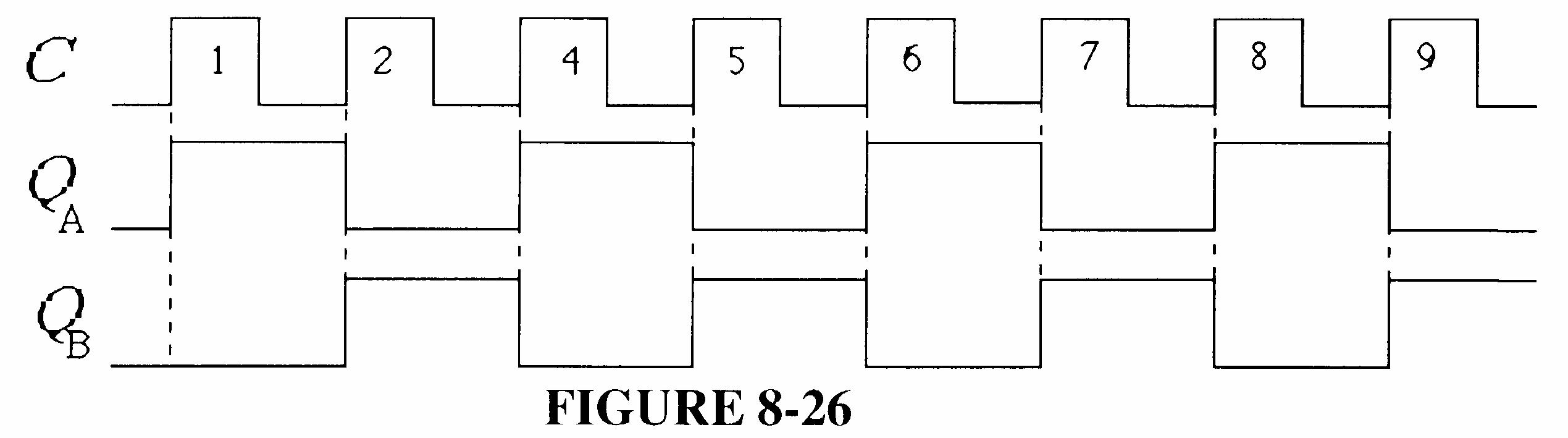
(c) See Figure 8-26.
8-26
(d) Normal operation because an open J input acts as a HIGH.
(e) A shorted K input will pull all J and K inputs LOW and the counter will not change from its initial state.
36. (a) Q0 and Q1 will not change from initial states.
(b) See Figure 8-27.
8-27
(c) See Figure 8-28.
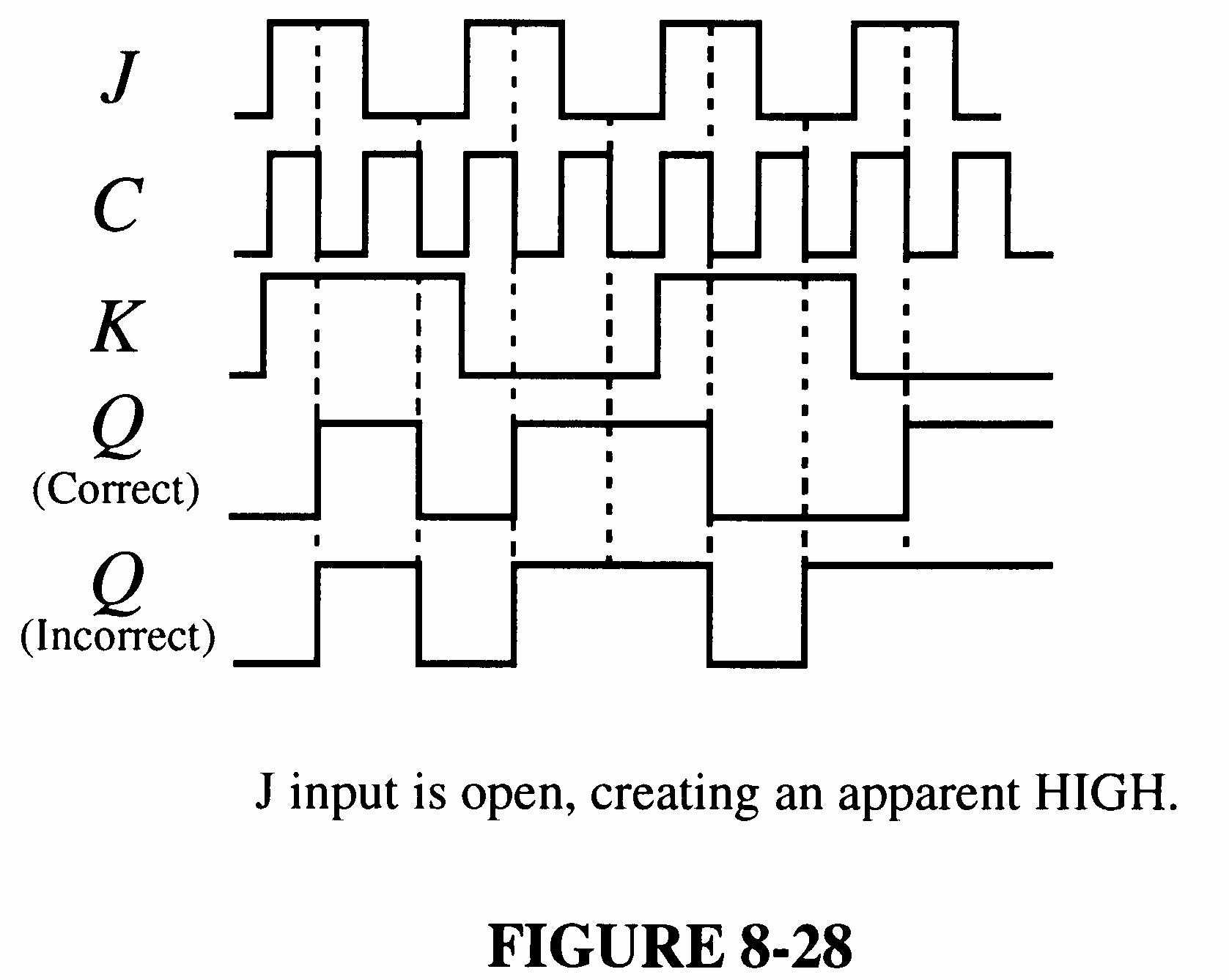
FIGURE 8-28
(d) Normal operation. See Figure 8-29.
FIGURE 8-29
(e) Both J and K of FF1 are pulled LOW if K is grounded, producing a no-change condition. Q0 also grounded. See Figure 8-30.
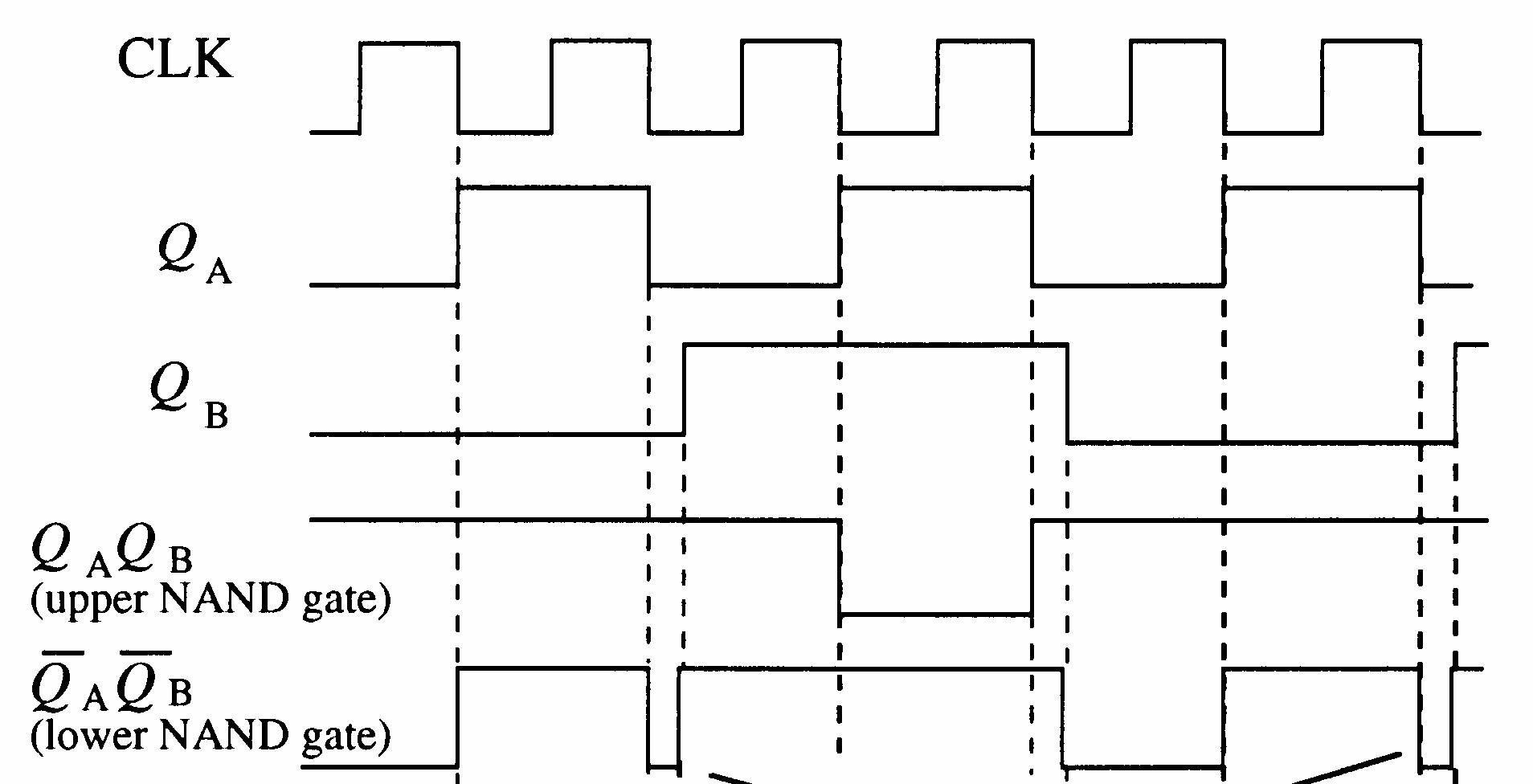
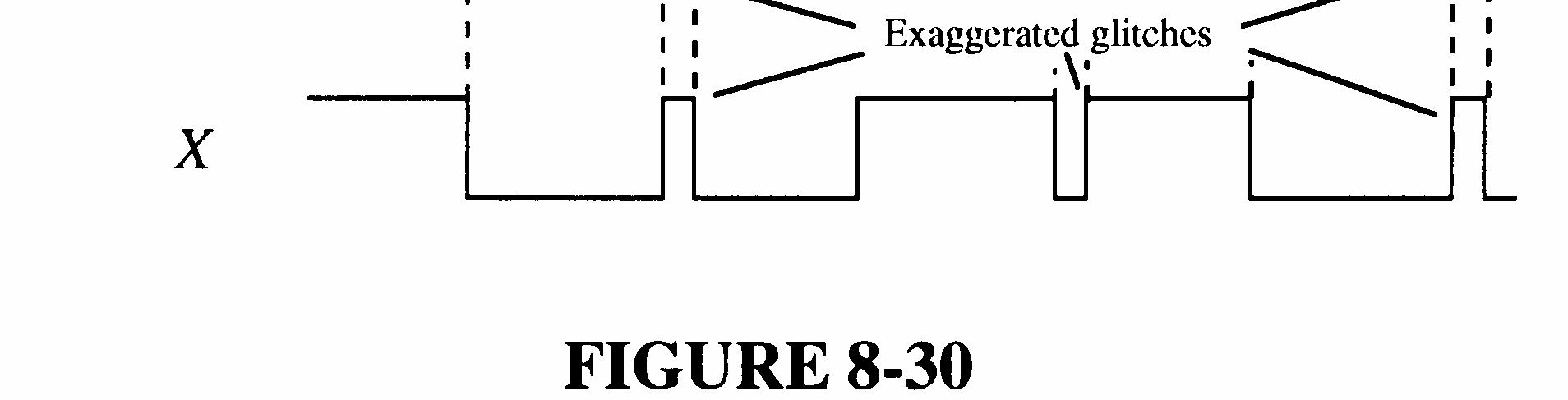
FIGURE 8-30
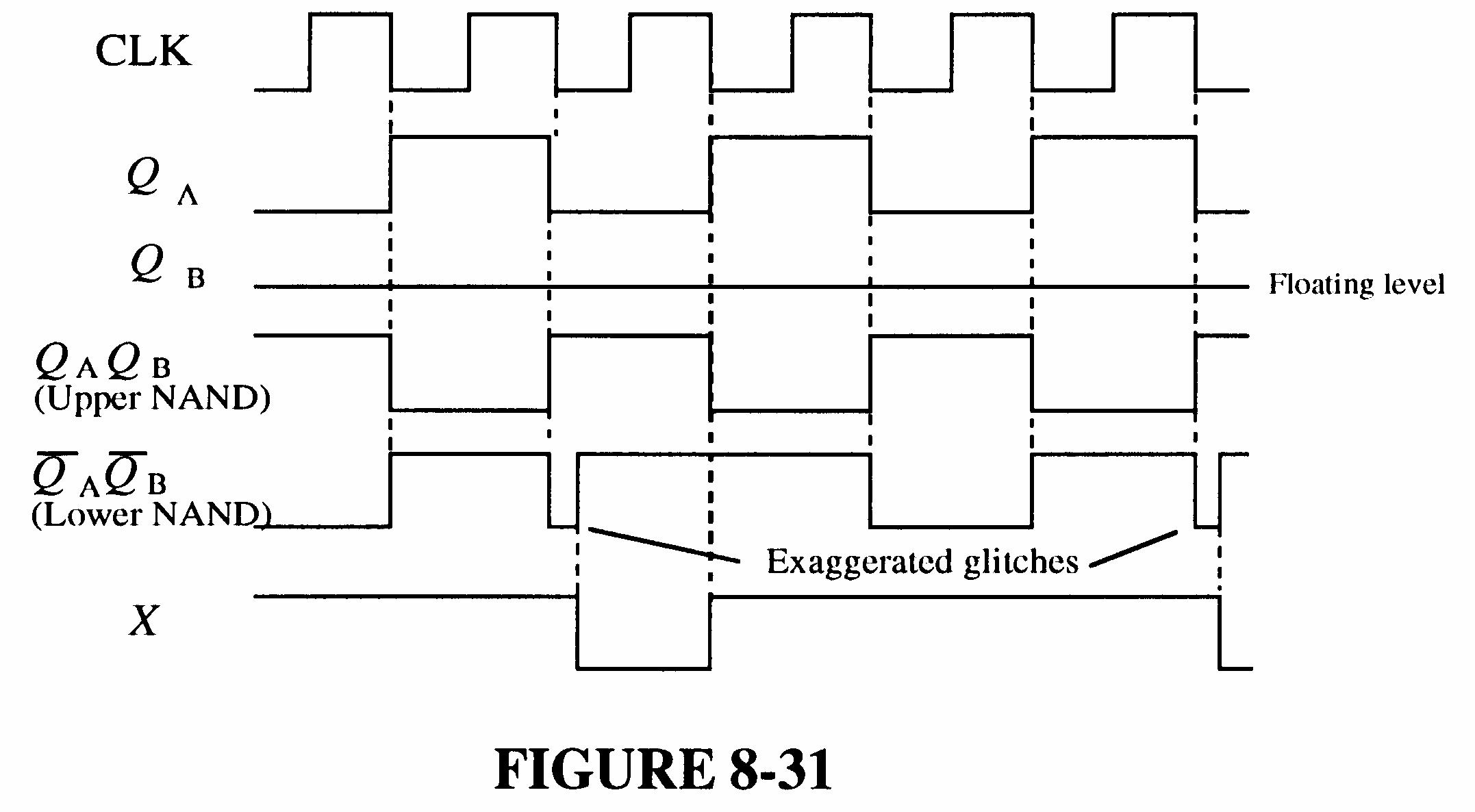
37. First, determine the correct waveforms and observe that Q0 is correct but Q1 and Q2 are incorrect in Figure 8-83 in the text. See Figure 8-31.
Since Q1 goes HIGH and stays HIGH, FF1 must be in the SET state (J = 1, K = 0). There must be a wiring error at the J and K inputs to FF1; K must be connected to ground rather than to the J input.
FIGURE 8-31
38. Since Q2 toggles on each clock pulse, its J and K inputs must be constantly HIGH. The most probable fault is that the AND gate’s output is open
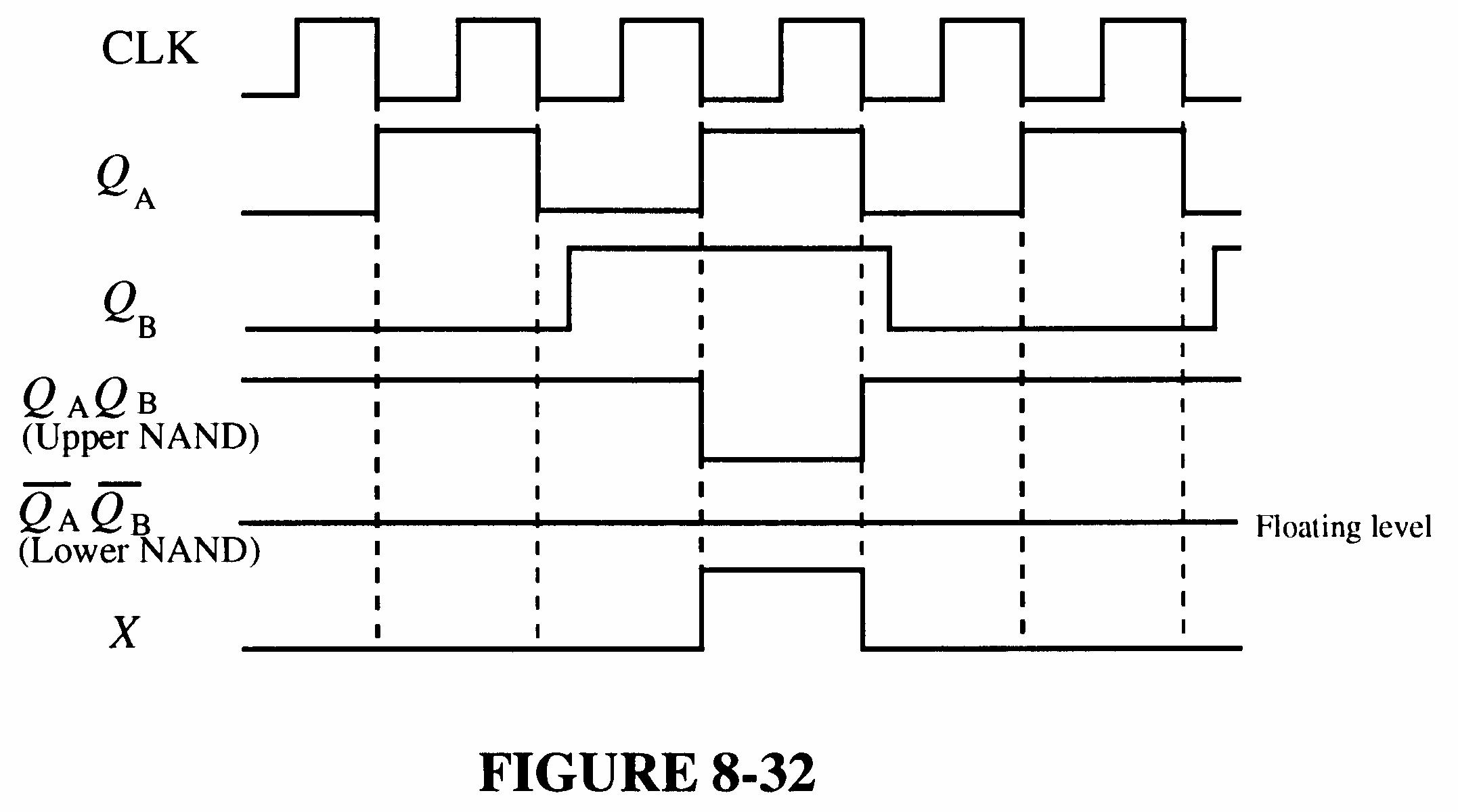
39. If the Q0 input to the AND gate is open, the JK inputs to FF2 are as shown in Figure 8-32.
FIGURE 8-32
40. Number of states = 40,000 fout = 40,000 MHz 5 = 125 Hz
41.
76.2939 Hz is not correct. The faulty division factor is Hz
76.2939 MHz 5 = 65,536
Obviously, the counter is going through all of its states. This means that the 63C016 on its parallel inputs is not being loaded. Possible faults are:
Inverter output is stuck HIGH or open.
RCO output of last counter is stuck LOW.
Hz
250.100 Hz
Hz
42. The flip-flop output is stuck HIGH or open.
The least significant BCD/7-segment input is open.
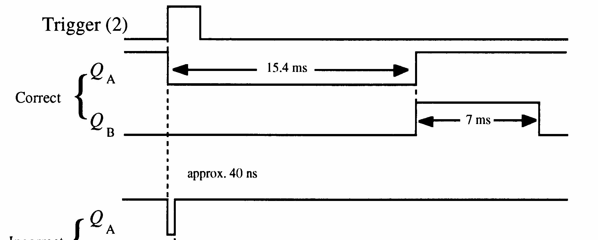
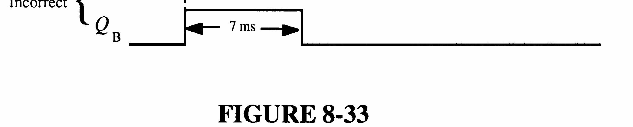
See Figure 8-33.
8-33
43. Th DIV 6 is the tens of minutes counter. Q1 open causes a continuous apparent HIGH output to the decode 6 gate and to the BCD/7-segment decoder/driver.
The apparent counter sequence is shown in the table.
The decode 6 gate interprets count 4 as a 6 (0110) and clears the counter back to 0 (actually 0010). Thus, the apparent (not actual) sequence is as shown in the table.
44. There are several possible causes of the malfunction. First check power to all units. Other possible faults are listed below.
Sensor Latch
Action: Disconnect entrance sensor and pulse sensor input.
Observation: Latch should SET.
Conclusion: If latch does not SET, replace it.
NOR gate
Action: Pulse sensor input.
Observation: Pulse on gate output.
Conclusion: If there is no pulse, replace gate.
Counter
Action: Pulse sensor input.
Observation: Counter should advance.
Conclusion: If counter does not advance, replace it.
Output Interface
Action: Pulse sensor input until terminal count is reached.
Observation: FULL indication and gate lowered
Conclusion: No FULL indication or if gate does not lower, replace interface.
Sensor/Cable
Action: Try to activate sensor.
Observation: If all previous checks are OK, sensor or cable is faulty.
Conclusion: Replace sensor or cable.
45. The expressions for the D0 and the D1 flip-flop inputs in the sequential logic portion of the system were developed in the System Application Activity. Figure 8-34 shows the NAND implementation.
D0 = S L S L V T Q V T Q Q Q 0 1 0 1 + +
D1 = S L T Q T Q 1 0 +
8-34
46. See Figure 8-35.
8-35
47. The time interval for the green light can be increased from 25 s to 60 s by increasing the value of either the resistor or the capacitor value by
s 60 = 2.4 times
s 25
48. See Figure 8-36.
8-36
49. 65,536 30,000 = 35,536
Preset the counter to 35,536 so that it counts from 35,536 up to 65,536 on each full cycle, thus producing a sequence of 30,000 states (modulus 30,000).
35,536 = 10001010110100002 = 8AD016
See Figure 8-37.
50. 65,536 50,000 = 15,536
9-35
8-37
Preset the counter to 15,536 so that it counts from 15,536 up to 65,536 on each full cycle, thus producing a sequence of 50,000 states (modulus 50,000).
15,536 = 111100101100002 = 3CB016
See Figure 8-38.
51. The approach is to preset the hours and minutes counters independently, each with a fast or slow preset mode. The seconds counter is not preset. One possible implementation is shown in Figure 8-39.
52. See Figure 8-40.
53. See Figure 8-41.
8-40
8-41
54. See Figure 8-42.
55. NEXT-STATE TABLE
TRANSITION TABLE
See Figure 8-43.
8-43
56. See Figure 8-44.
57. Q output of U3 open.
58. SET input of U1 open.
59. Pin A of G3 open.
60. No fault.
61. Pin 9 open.
Section 9-1 Basic Shift Register Operations
1. Shift registers store binary data in a series of flip-flops or other storage elements.
2. 1 byte = 8 bits; 2 bytes = 16 bits
3. Shift data and store data
Section 9-2 Serial In/Serial Out Shift Registers
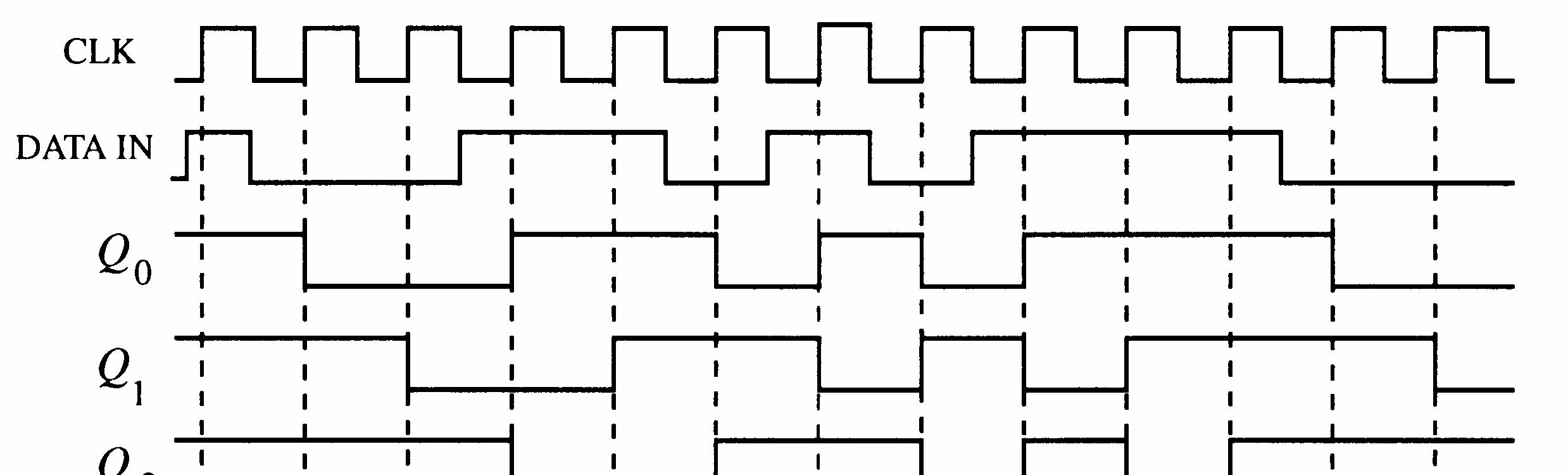
4. Initially: 0000 1st CLK: 1000 2nd CLK: 1100 3rd CLK: 0110
5. See Figure 9-1.
6. See Figure 9-2.
Initially 101001111000
CLK 1
CLK 2
CLK 3
CLK 4
CLK 5
CLK 6
CLK 7
CLK 8
CLK 9
CLK 10
CLK 11
CLK 12
010100111100
001010011110
000101001111
000010100111
100001010011 110000101001 111000010100 011100001010
001110000101
000111000010
100011100001 110001110000
8. See Figure 9-3.
FIGURE 9-3
9. See Figure 9-4.
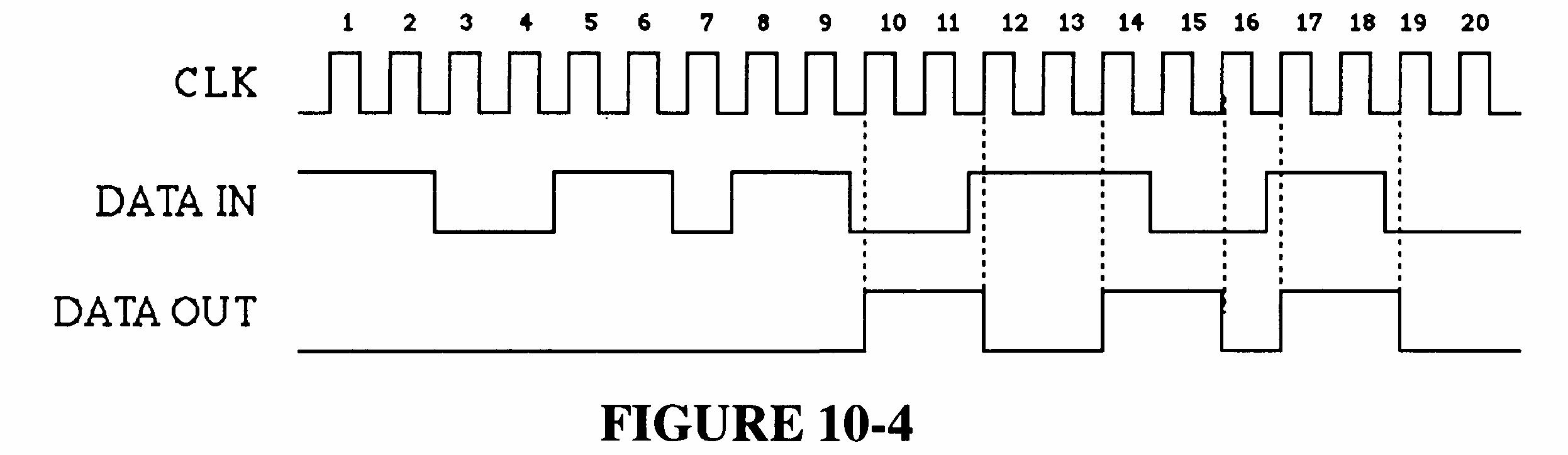
FIGURE 9-4
10. See Figure 9-5.
9-5
Section 9-3 Serial In/Parallel Out Shift Registers
11. See Figure 9-6.
12. See Figure 9-7.
13. See Figure 9-8.
9-8
14. See Figure 9-9.
9-9
15. See Figure 9-10.
9-10
16. See Figure 9-11.
9-11
17. See Figure 9-12.
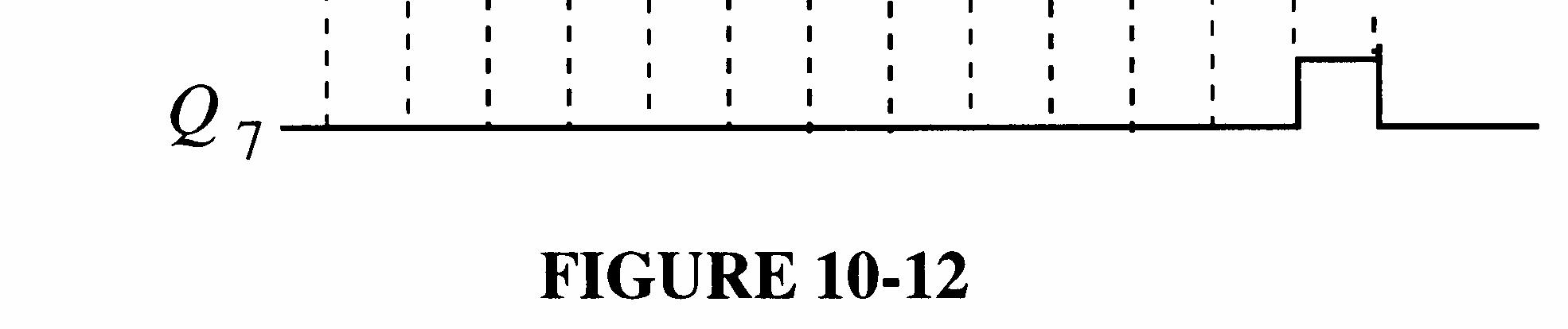
FIGURE 9-12
Section 9-5 Parallel In/Parallel Out Shift Registers
18. See Figure 9-13.
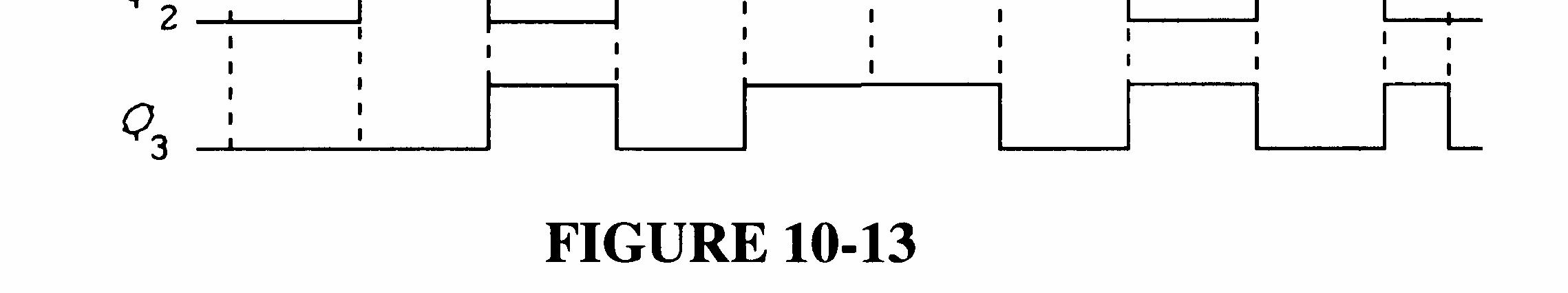
FIGURE 9-13
19. See Figure 9-14.
9-14
20. See Figure 9-15.
9-15
21. Initially (76)
CLK 1
CLK 2
CLK 3
CLK 4
CLK 5
CLK 6
CLK 7
CLK 8
CLK 9
CLK 10
CLK 11
22. Initially (76)
CLK 1
CLK 2
CLK 3
CLK 4
CLK 5
CLK 6
CLK 7
CLK 8
CLK 9
CLK 10
CLK 11
CLK 12
23. See Figure 9-16.
Shift left
Shift right
Shift right
Shift right
Shift right
Shift left
Shift right
Shift left
Shift left
Shift left
Shift right
Shift right
9-16
24. See Figure 9-17.
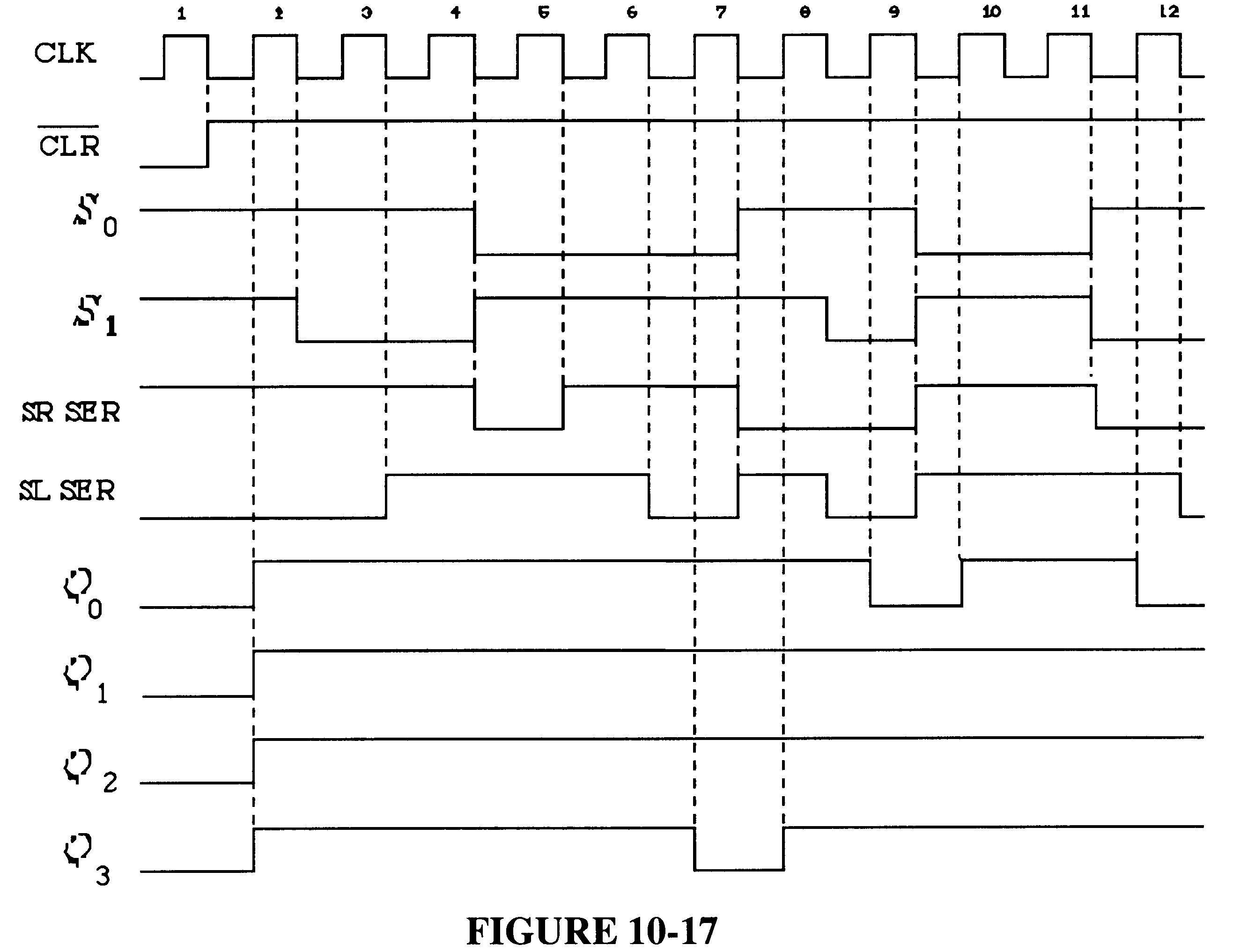
FIGURE 9-17
25. (a) 2n = 6 (b) 2n = 10 n = 3 n = 5 (c) 2n = 14 (d) 2n = 16 n = 7 n = 8
26. 2n = 18; n = 9 flip-flops
See Figure 9-18.
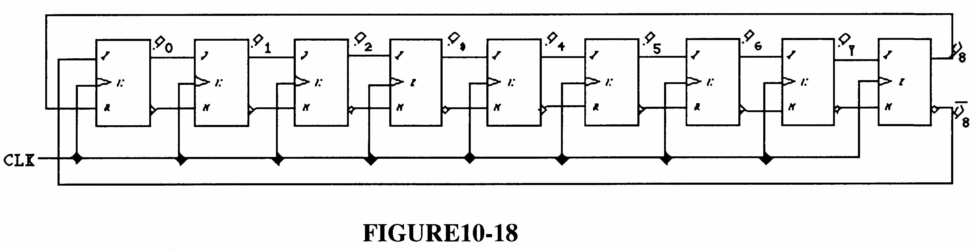
FIGURE 9-18
27. See Figure 9-19.
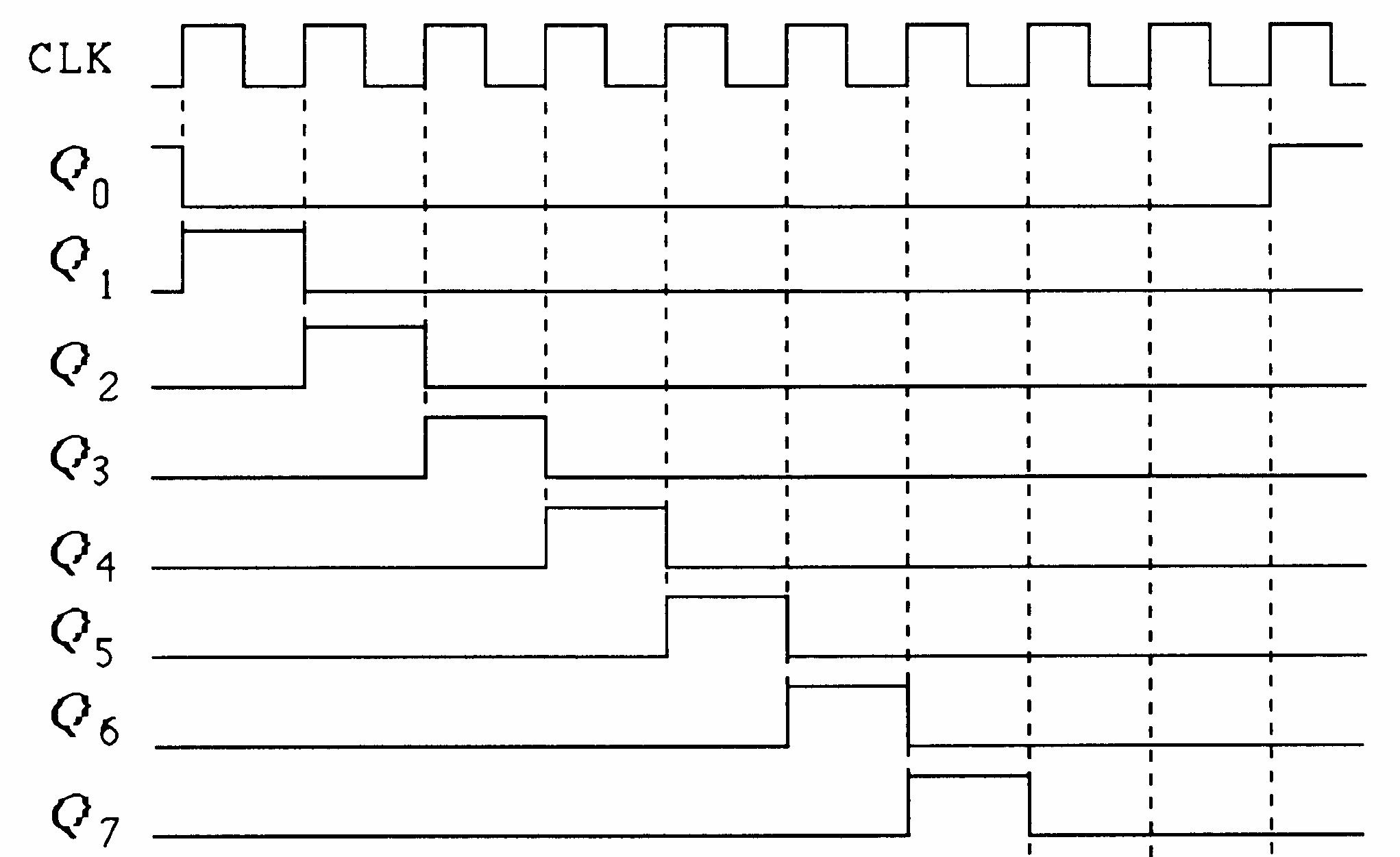
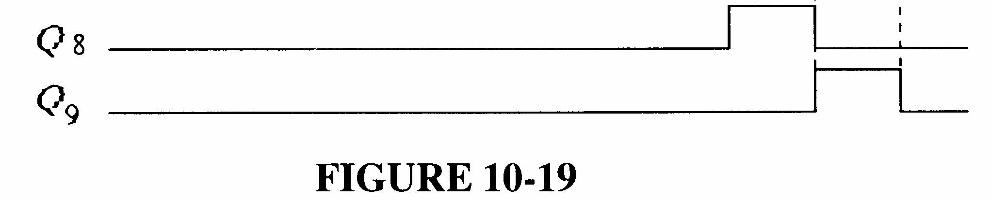
FIGURE 9-19
28. A 15-bit ring counter with stages 3, 7, and 12 SET and the remaining stages RESET. See Figure 9-20.
9-20
29. See Figure 9-21.
30. The power-on LOAD input provides a momentary LOW to parallel load the ring counter when power is turned on.
31. An incorrect code may be produced.
32. Q2 goes HIGH on the first clock pulse indicating that the D input is open. See Figure 9-22.
33. Since the LSB flip-flop works during serial shift, the problem is most likely in gate G3. An open D3 input at G3 will cause the observed waveform. See Figure 9-23.
9-23
34. It takes a LOW on the RIGHT/LEFT input to shift data left. An open inverter input will keep the inverter output LOW thus disabling all of the shift-left control gates G5, G6, G7, and G8.
35. (a) No clock at switch closure due to faulty NAND gate or one-shot; open clock input to key code register; open LD SH/input to key code register.
(b) The diode in the third row is open; Q2 output of ring counter is open.
(c) The NAND (negative-OR) gate input connected to the first column is shorted to ground or open, preventing a switch closure transition.
(d) The “2” input to the column encoder is open.
36. 1. Number the switches in the matrix according to the following format:
2. Depress switches one at a time and observe the key code output according to the following Table 1.
TABLE 1
37. (a) Contents of Data Output Register remain constant. (b) Contents of both registers do not change.
(c) Third stage output of Data Output Register remains HIGH. (d) Clock generator is disabled after each pulse by the flip-flop being continuously SET and then RESET.
38. The purpose of the Security Code logic is to accept a 4-digit code, compare it with a stored code, and if the codes match, to disarm the system for entry.
39. The states of shift registers A and C after two correct key closures are:
Shift Register A: 1001
Shift Register C: 00000100
40. The states of shift registers A and B after each key closure when entering 7645 are:
After key 7 is pressed:
Shift register A contains 0111
Shift register B contains 11000
After key 6 is pressed:
Shift register A contains 0110
Shift register B contains 11100
After key 4 is pressed:
Shift register A contains 0100
Shift register B contains 11110
After key 5 (an incorrect entry) is pressed:
Shift register A contains 0000
Shift register B contains 10000
41. See Figure 9-24.
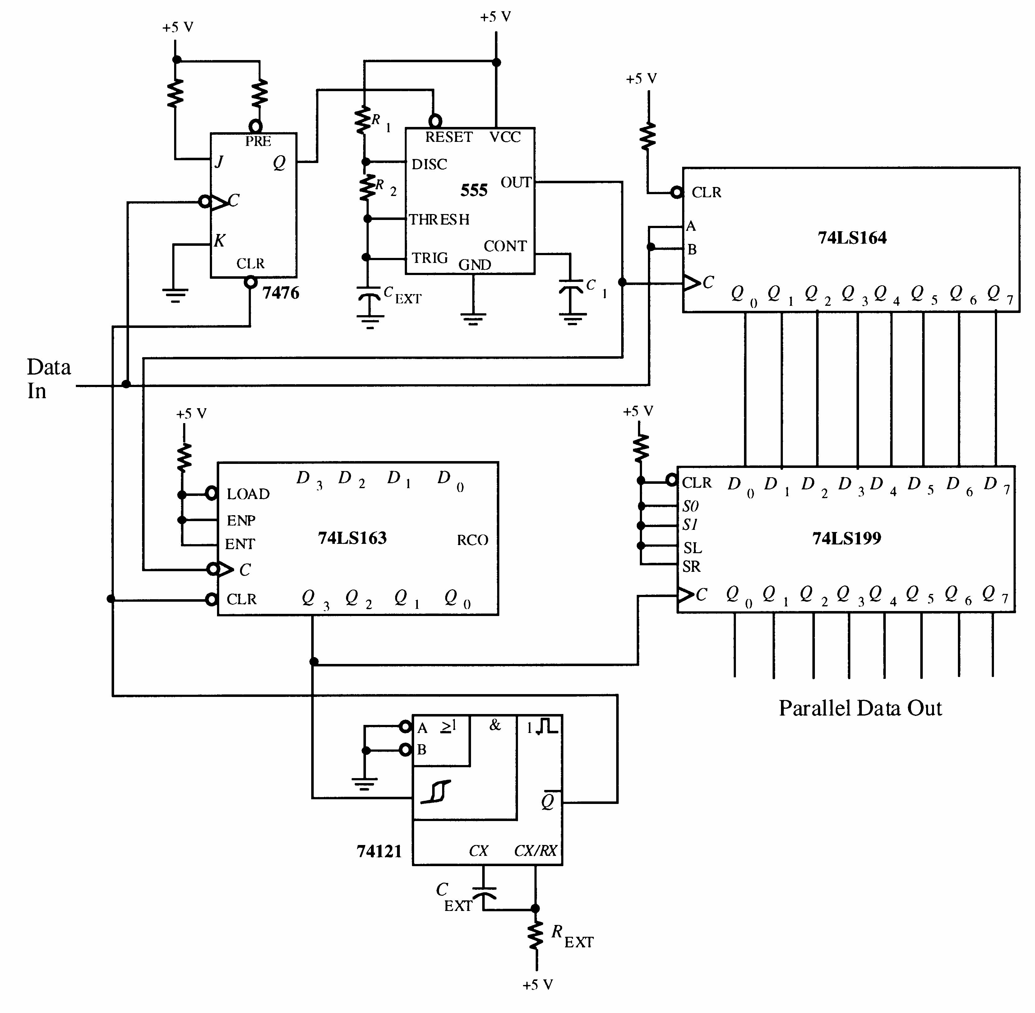
42. Figure 9-25 shows only the 74LS164, 74LS199, and 74LS163 portions of the circuit that require modification for 16-bit conversion.
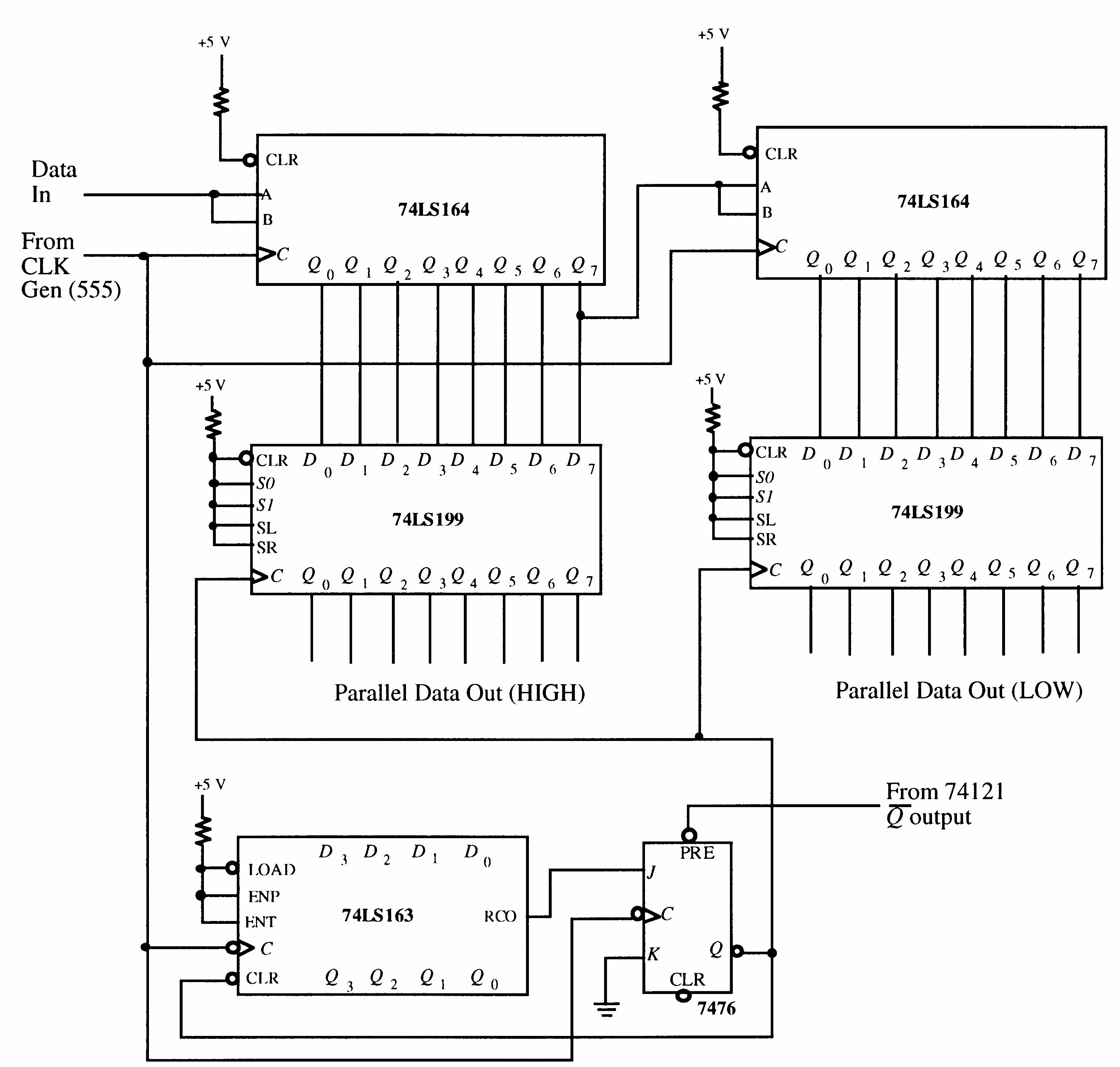
9-25
43. See Figure 9-26 for one possible implementation.
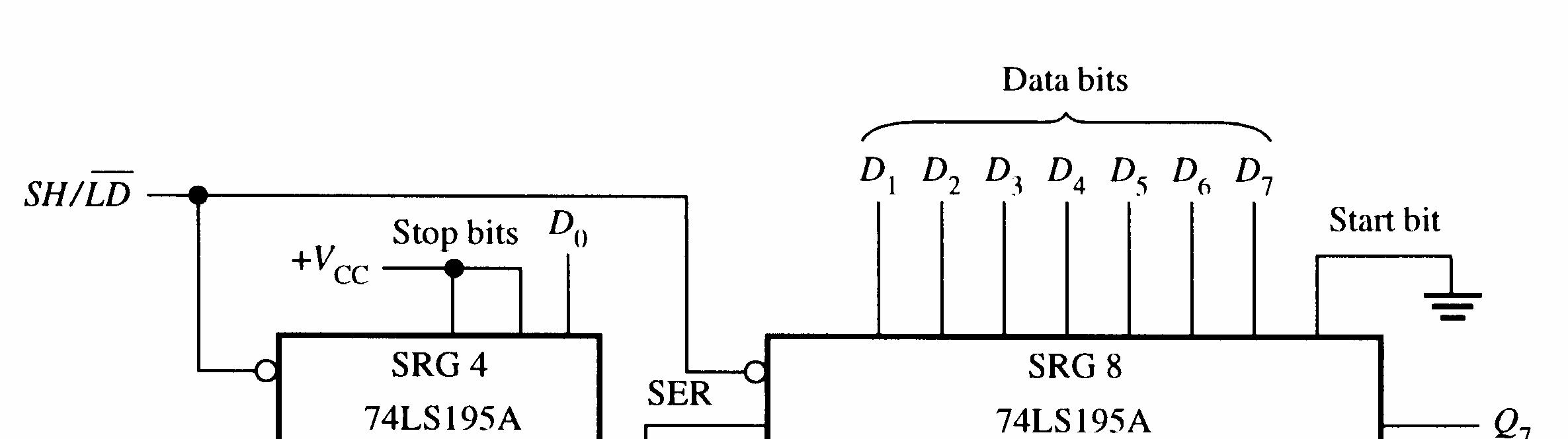
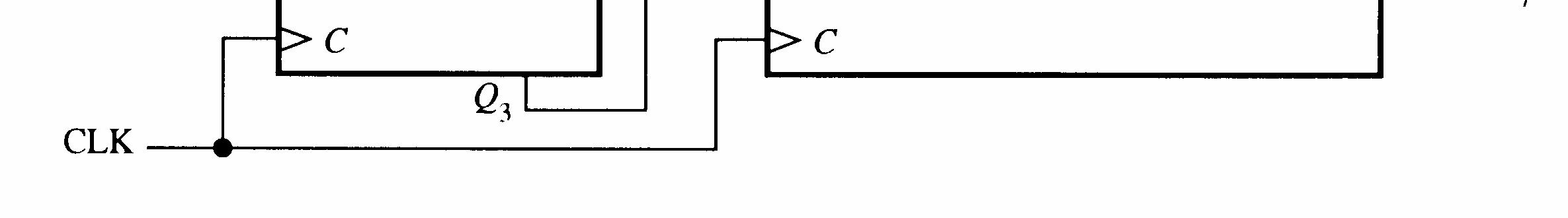
9-26
44. One possible approach is shown in Figure 9-27.
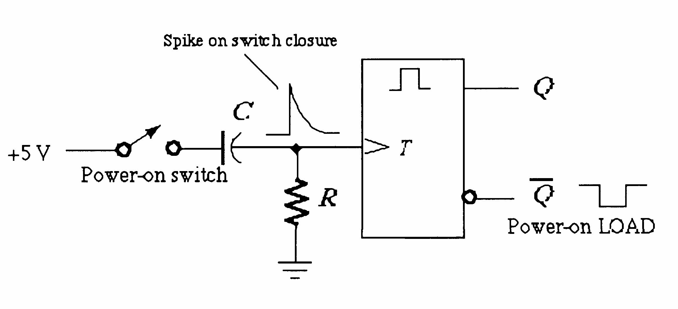

45. See Figure 9-28.
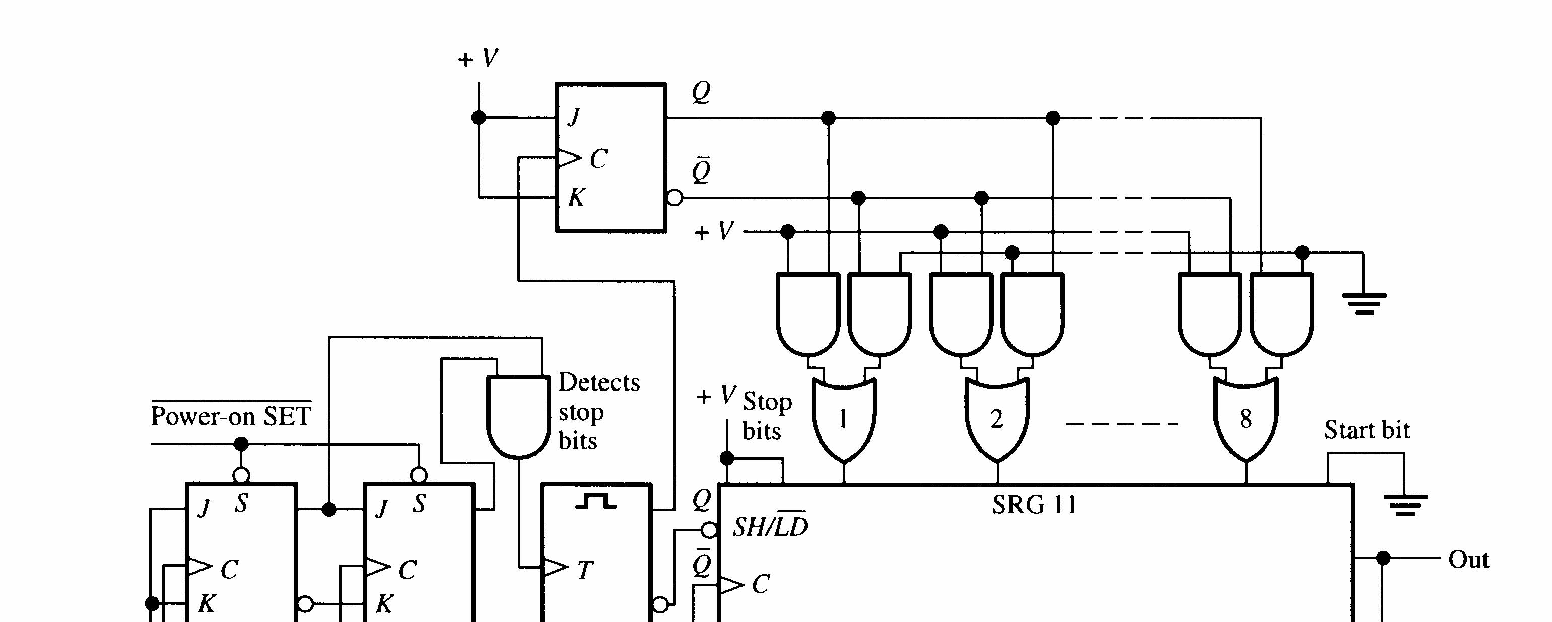
46. Register A requires 8 bits and can be implemented with one 74199. Register B requires 16 bits and can be implemented with two 74199s.
47. CLK input of U3 open.
48. No fault.
49. Pin 14 open.
50. No fault.
51. CLK input of U6 open.
1. (a) ROM: no read/write control (b) RAM
2. They are random access memories because any address can be accessed at any time. You do not have to go through all the preceding addresses to get to a specific address.
3. Address bus provides for transfer of address code to memory for accessing any memory location in any order for a read or a write operation. Data bus provides for transfer of data between the microprocessor and memory or input/output devices.
4. (a) 0A16 = 000010102 = 1010 (b) 3F16 = 001111112 = 6310 (c) CD16 = 110011012 = 20510
5.
6. See Figure 10-1.
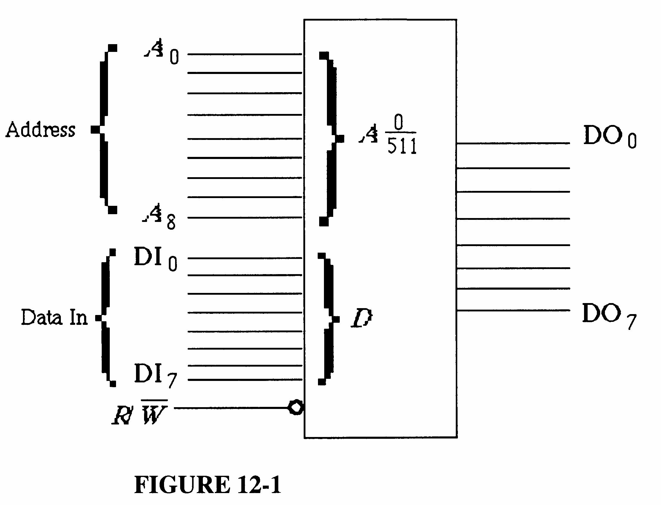
10-1
64k × 8 = 512 × 128 × 8 = 512 rows × 128 8-bit columns
8. See Figure 10-2.
9. The difference between SRAM and DRAM is that data in a SRAM are stored in latches or flip-flops indefinitely as long as power is applied while data in a DRAM are stored in capacitors which require periodic refreshing to retain the stored data.
10. The bit capacity of a DRAM with 12 address lines is 22 × 12 = 224 = 16,777,216 bits = 16 Mbits
Section 10-3 The Read-Only
11.
12.
13.
BCD
See Figure 10-3.
14. 214 = 16,384 addresses 16,384 × 8 bits = 131,072 bits
Excess-3
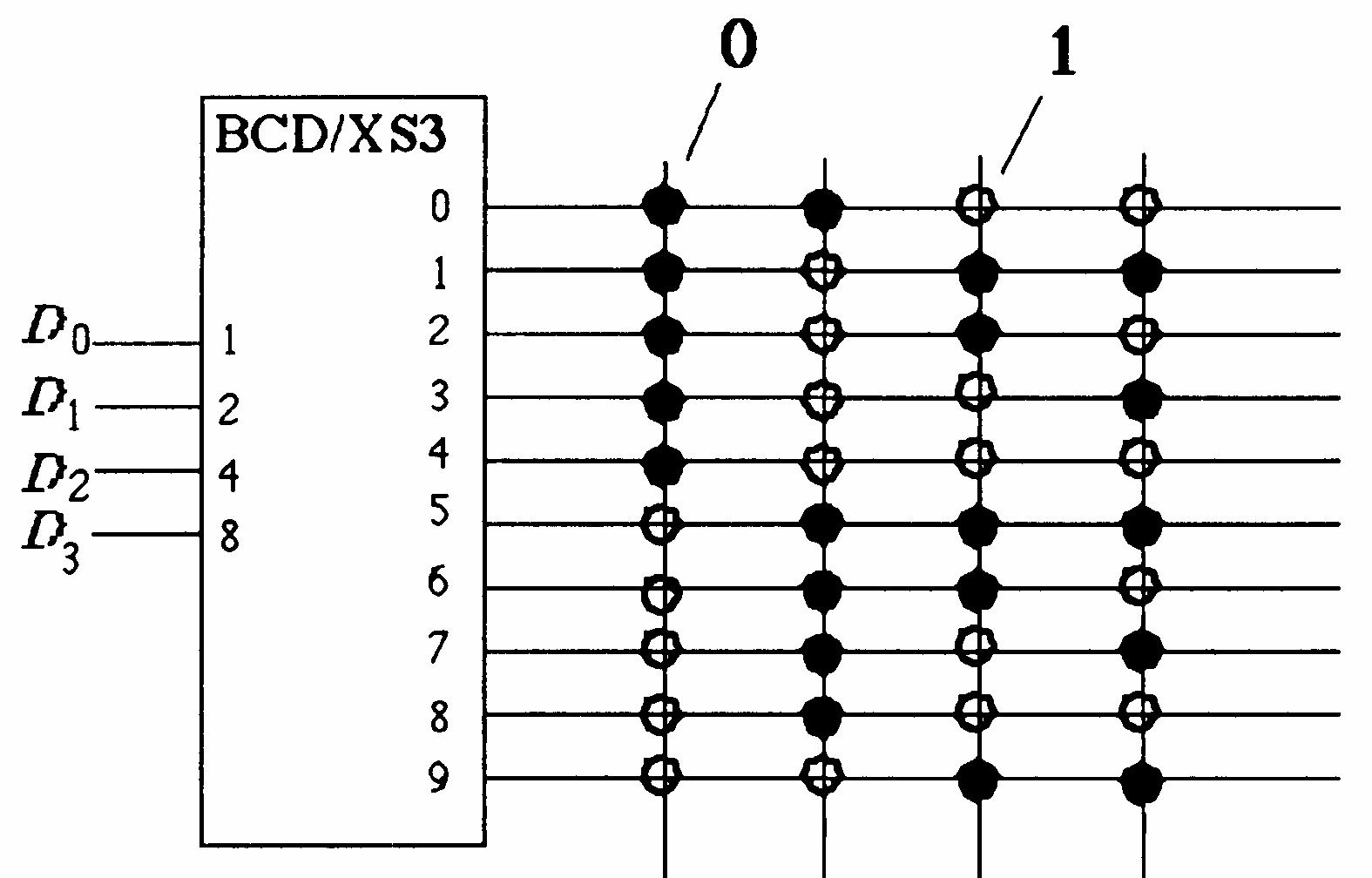
FIGURE 10-3
15. Blown links: 1 17, 19 23, 25 31, 34, 37, 38, 40 47, 53, 55, 58, 61, 62, 63, 65, 67, 69.
16. Address A13 A0 Contents Q7 Q0 01001100010011 11011101011010 01011010011001 11010010001110 01010010100101 01010000110100 01001001100001 11011011100100 01101110001111 10111110011010 10101110011010 10101100 00100101 10110011 00101000 10001011 11010101 11001001 01001001 01010010 01001000 11001000
17. 16k × 4 DRAMS can be connected to make a 64k × 8 DRAM as shown in Figure 10-4.
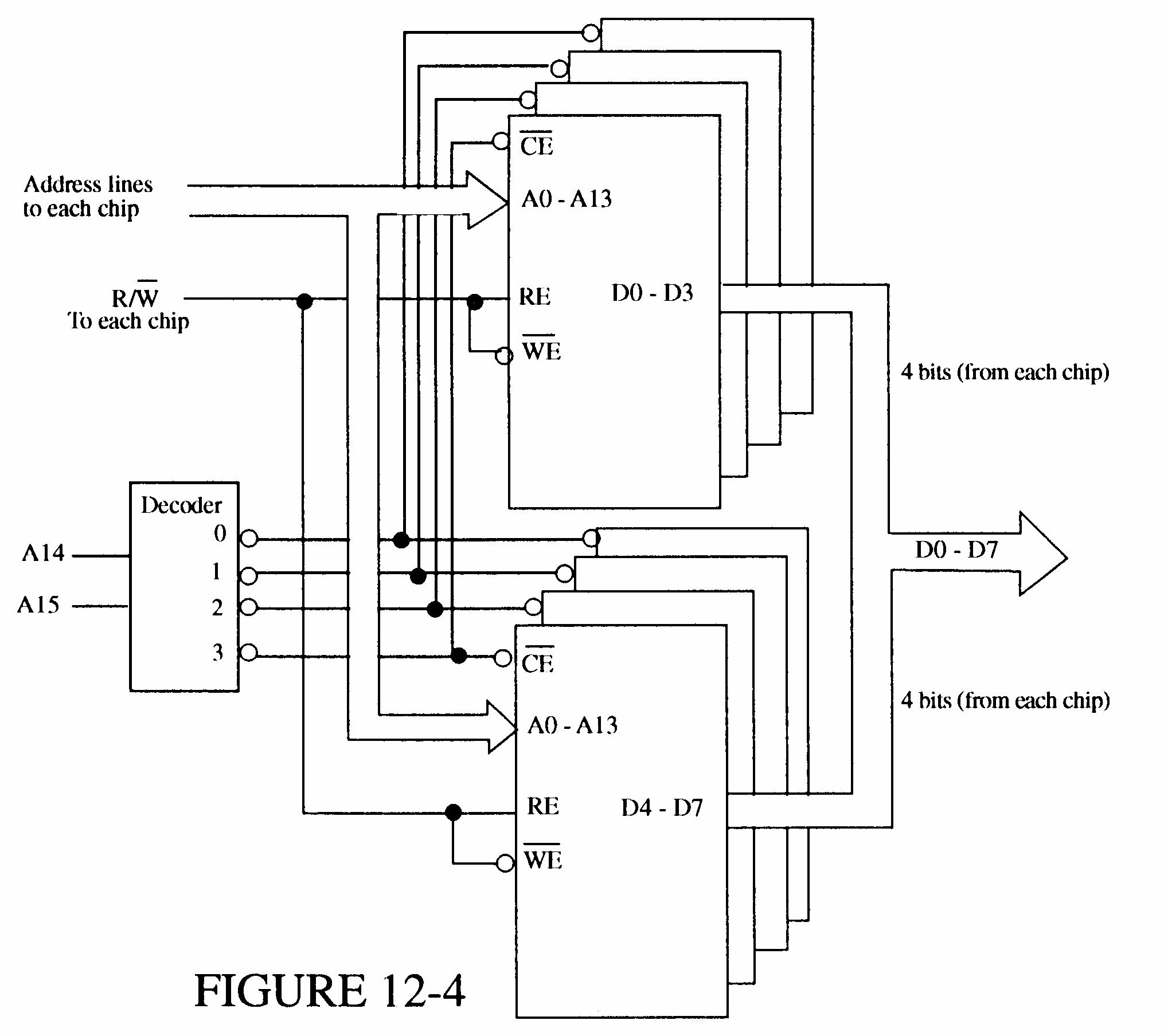
FIGURE 10-4
18. See Figure 10-5.
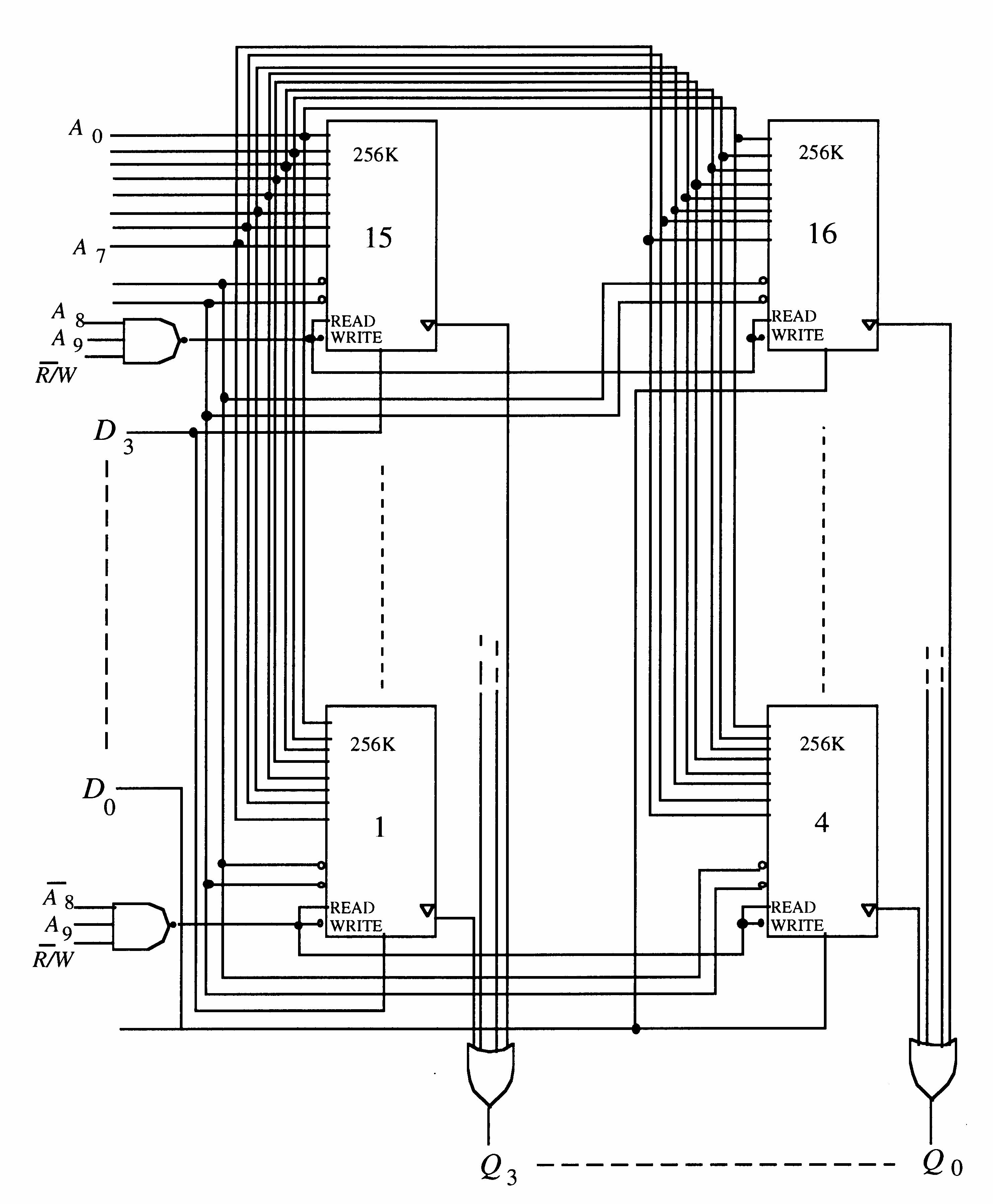
FIGURE 10-5
19. Word length = 8 bits, word capacity = 64k words
Word length = 4 bits, word capacity = 256k words
20. See Figure 10-6.
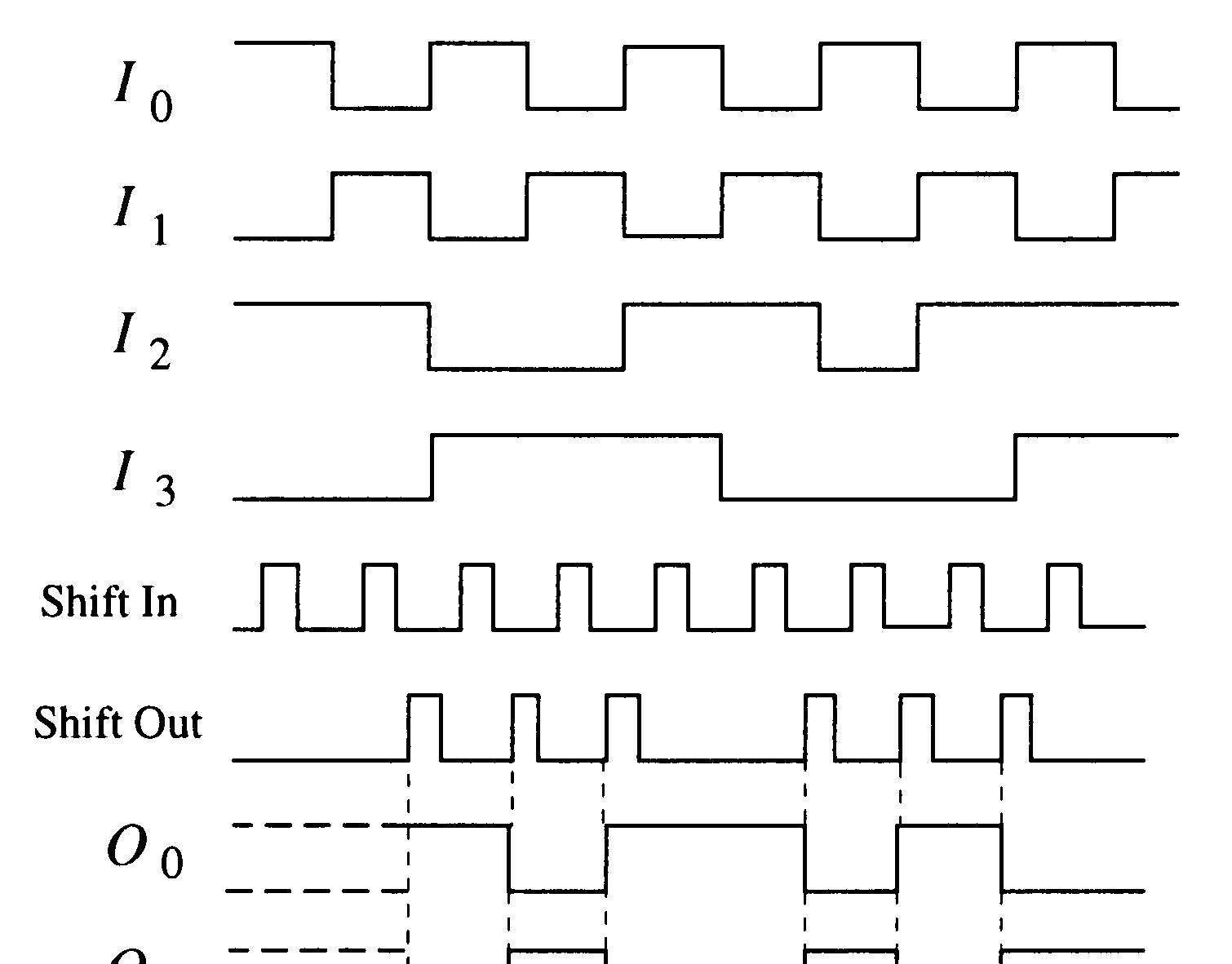
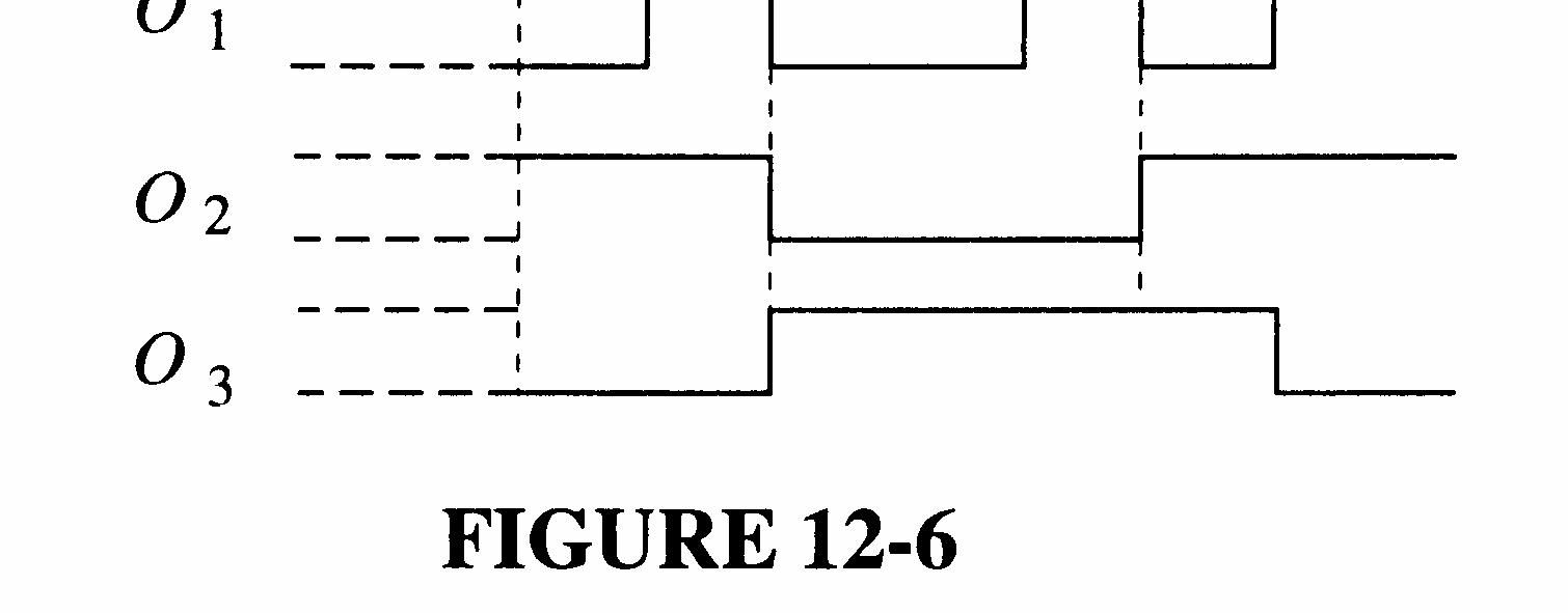
10-6
21. See Figure 10-7.
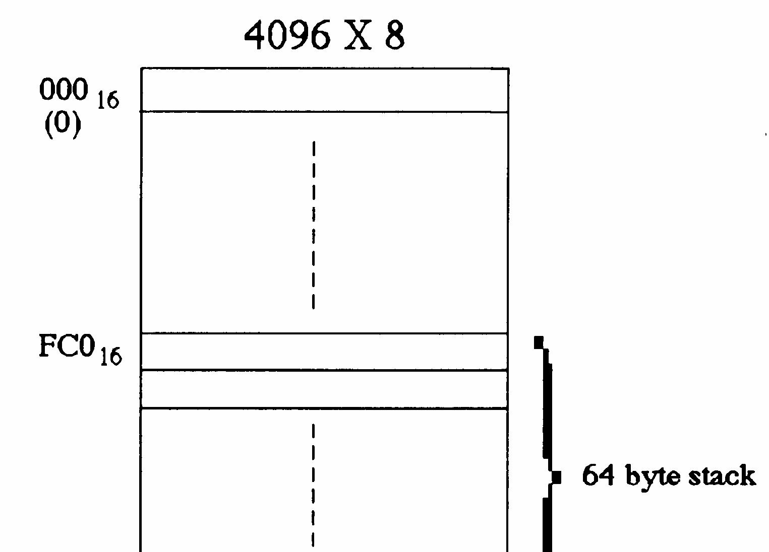
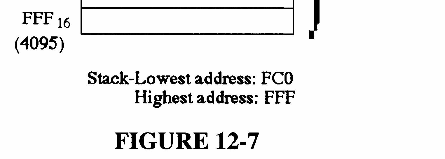
10-7
22. The first byte goes into FFF16 The last byte (16th) goes into a lower address: 1610 = 1016 FFF16 1016 = FEF16
See Figure 10-8.
23. A hard disk is formatted into tracks and sectors. Each track is divided into a number of sectors with each sector of a track having a physical address. Hard disks typically have from a few hundred to a few thousand tracks.
24. Seek time is the average time required to position the drive head over the track containing the desired data. The latency period is the average time required for the data to move under the drive head.
25. Magnetic tape has a longer access time than disk because data must be accessed sequentially rather than randomly.
26. A magneto-optic disk is a read/write medium using lasers and magnetic fields. A CD-ROM (compact-disk ROM) is a read-only optical (laser) medium. A WORM (write-once-read-many) is an optical medium in which data can be written once and read many times.
27. The correct checksum is 00100. The actual checksum is 01100. The second bit from the left is in error.
28. (a) ROM0: Low address - 0016 High address - 1F16
ROM1: Low address - 2016 High address - 3F16
ROM2: Low address - 4016 High address - 5F16
ROM3: Low address - 6016 High address - 7F16
(b) Same as flow chart in Figure 10-68 in text except that the last data address is specified as 7E16 (7F16 1).
(c) See Figure 10-9.
Compare checksum with final XOR sum of data Read checksum address
Do they agree? Indicate fault
(d) A single checksum will not isolate the faulty chip. It will only indicate that there is an error in one of the chips.
29. (a) 4016 5F16 is 64 95 decimal; ROM 2
(b) 2016 3F16 is 32 63 decimal; ROM 1
(c) 0016 7F16 is 0 127 decimal; All ROMs
30. See Figure 10-10.
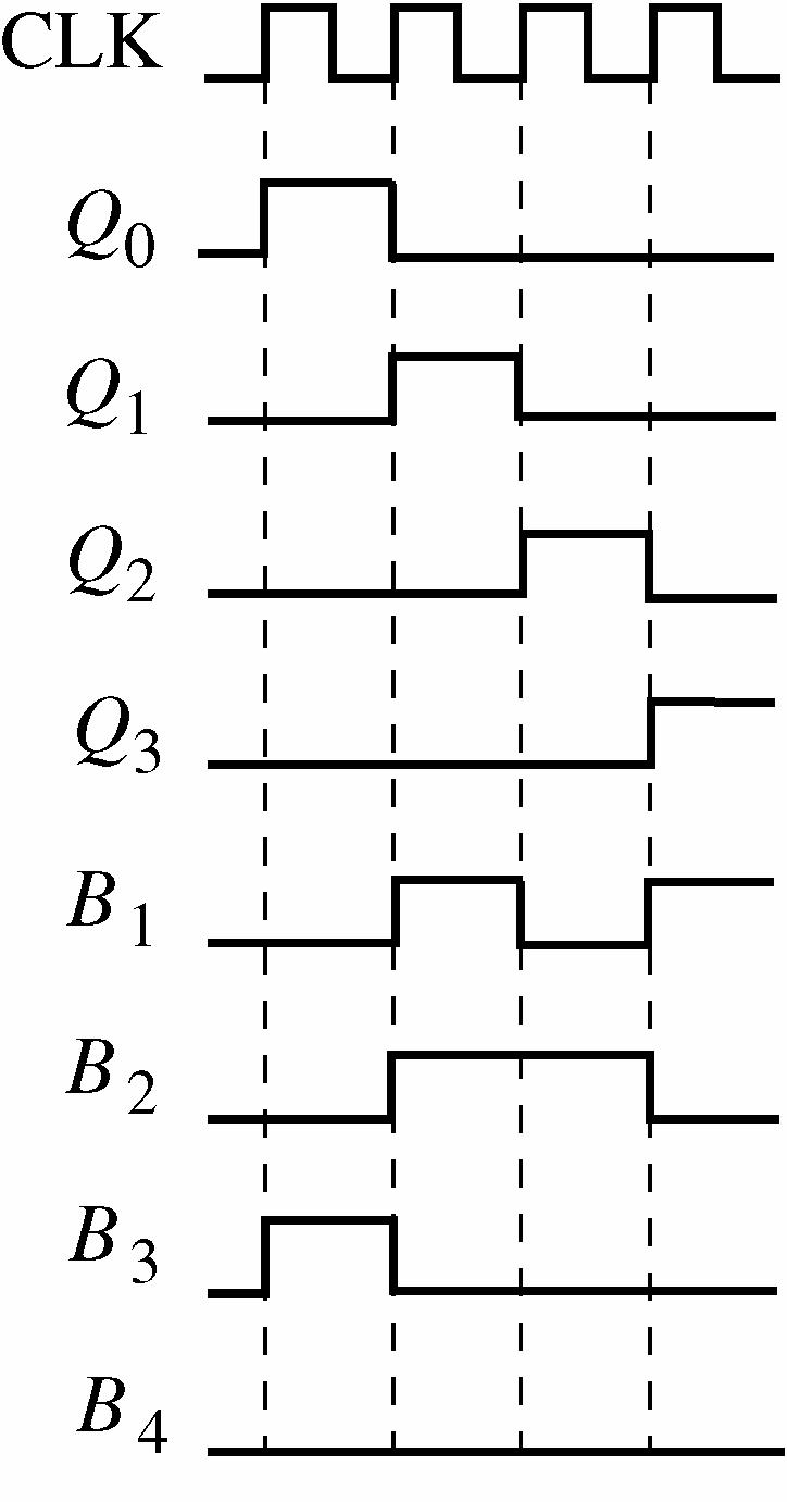
31. On first digit entry, the register state is 0001. On second digit entry the register state is 0010.
32. The purpose of the switch memory is to store a 4-digit security code and permit easy code change.
33. A new code can be entered by simply moving the DIP switch settings. No power is required.
34. NAND gates U1A-U4D: four 74HC00
NAND gates U5A-U6B: two 74HC20
Shift register U7: 74HC195
35. See Figure 10-11.
Section 11-1 Programmable Logic: SPLDs and CPLDs
1. . X ABCABCABC=++ See Figure 11-1.
2. See Figure 11-2.
FIGURE 6-2
(b)Cannot be implemented as stated because it has 4 product terms. Simplify to: X=AC + AB
3. (a) PAL16L2 is a programmable array logic device with 16 inputs and two active-LOW outputs.
(b) PAL12H6 is a programmable array logic device with 12 inputs and 6 active-HIGH outputs.
4. Typically, an exclusive-OR gate is used to determine the polarity of the output. When a 1 is applied to one input of the XOR gate, the output of the XOR is the complement of the signal on the other input. When a 0 is applied to one input of the XOR, the signal on the output of the XOR is the same as the signal on the other input.
5. A CPLD basically consists of multiple SPLDs that can be connected with a programmable interconnect array.
6. (a) Inputs from PIA to LAB: 36 (b) Outputs from LAB to PIA: 16 (c) Inputs from I/O to PIA: 8 to 16 (d) Outputs from LAB to I/O: 8 to 16
7. (a) ABCD (b) ()() ABCDEABCDEABCDABCE =+=+
8. ABCDEFGHABCDABCD +++
9. ABAB +
10. (a) Inputs from AIM to FB: 40 (b) Outputs from FB to AIM: 16 (c) Inputs from I/O to AIM: 16 (d) Outputs from FB to I/O: 16
11. X1 = ; A BCDABCDABCD ++ X2 = ABCDABCDABCDABCD +++
12. (a) A 0 on the select line selects D0. The output is 1. (b) A 1 on the select line selects D1. The output is 0.
13. (a) Since the D0 (upper) input of MUX 5 is selected, the macrocell is configured for combinational logic. The output of the XOR goes through MUX 5 to the “To I/O” output making it a 1.
(b) Since the D1 (lower) input of MUX 5 is selected, the macrocell is configured for registered logic. The output of the flip-flop goes through MUX 5 to the “To I/O” output making it a 0.
14. (a) The macrocell is configured for registered logic because the D1 input of MUX 8 is selected, allowing the flip-flop output to pass through.
(b) The GCK1 clock is applied to the flip-flop because the D1 input of MUX 3 and the D1 input of MUX 5 are selected.
(c) The OR gate output is applied to the XOR which is set for noninversion by MUX 1. The output of the XOR is selected by MUX2 and a 1 is applied to the D/T input of the flipflop.
(d) The output of MUX 8 is a 1 because MUX 8 selects the Q output of the flip-flop (assuming that the S and R inputs are 0).
15. (a) The macrocell is configured for registered logic because the D1 input of MUX 8 is selected, allowing the flip-flop output to pass through.
(b) The GCK1 clock is applied to the flip-flop because the D1 input of MUX 3 and the D1 input of MUX 5 are selected.
(c) The OR gate output is applied to the XOR which is set for inversion by MUX 1. The output of the XOR is selected by MUX 2 and a 0 is applied to the D/T input of the flipflop.
(d) The output of MUX 8 is a 0 because MUX 8 selects the Q output of the flip-flop (assuming that the S and R inputs are 0).
16. An FPGA typically consists of configurable logic blocks (CLBs). Each CLB is made up of a number of logic modules with a local interconnect. Each logic module typically consists of a look-up table (LUT) and associated logic. Global column and row interconnects are used to connect the CLBs to I/Os as well as each other.
17. SOP output = ABCABCABCABCABC ++++
18. See Figure 11-3.
6-3
19. An ALM consists of an LUT for combinational logic, adder logic, and register logic.
20. The modes of operation of an ALM are: Normal, Extended LUT, Arithmetic, and Shared arithmetic.
21. See Figure 11-4.
22. 4321432105321532153210 ()() AAAAAAAAAAAAAAAAAAAAAA ++++ = 4321043210532105321053210A AAAAAAAAAAAAAAAAAAAAAAAA ++++
23. See Figure 11-5.
11-5
24. See Figure 11-6.
25. One slice. See Figure 11-7.
11-6
11-7
26. Three slices are required. See Figure 11-8.
11-8
27. See Figure 11-9.
11-9
28. X ABCDABCDABCDABCDABCDABCD =+++++ = ABDACDABCBCDABCD ++++
See Figure 11-10.
29. See Figure 11-11.
FIGURE 11-10
11-11
X
=++++ See Figure 11-12.
11-12
31. The Shift input = 1, data are applied to SDI, go through the MUX, and are clocked into Capture register A on the leading edge of the clock pulse. From the output of Capture register A, the data go through the upper MUX and are clock into Capture register B on the trailing edge of the clock pulse.
32. PDI/O = 0 and OE = 1. The data from the internal programmable logic pass through the selected MUX and through the output buffer to the pin.
33. PDI/O = 0 and OE = 0. The data are applied to the input pin and go through the selected MUX to the internal programmable logic.
34. SHIFT = 1, PDI/O = 1, and OE = 0. Data are applied to SDI, go through the MUX, and are clocked into Capture register A on the leading edge of the clock pulse. From the output of Capture register A, the data go through the upper MUX and are clocked into Capture register B on the trailing edge of the clock pulse. A pulse on the UPDATE input clocks the data into Update register B. The data on the output of Capture Register B go through the MUX to the internal programmable logic. The data also appear on the SDO.
35. 000011001010001111011 shifted from TDI to TDO, left-most bit first. The bold-faced code will appear on the logic inputs in the sequence shown.
0 000011001010001111011
1 000011001010001111011
3 000011001010001111011
6 000011001010001111011
12 000011001010001111011
9 000011001010001111011
2 000011001010001111011
5 000011001010001111011 10 000011001010001111011
4 000011001010001111011
8 000011001010001111011 1 000011001010001111011
3 000011001010001111011
7 000011001010001111011
15 000011001010001111011
14 000011001010001111011
13 000011001010001111011
11 000011001010001111011
36. 11 inverters can be eliminated. Only four are needed to produce the complements of A, B, C, and D
There are three AND gates that produce the product term . AC Two can be eliminated.
There are three AND gates that produce the product term AB Two can be eliminated.
There are two AND gates that produce the product term BC One can be eliminated.
There are two AND gates that produce the product term BC One can be eliminated.
There are two AND gates that produce the product term .AB One can be eliminated.
7 AND gates can be eliminated.
37. The D input to the logic is faulty or not connected. See Figure 11-13.

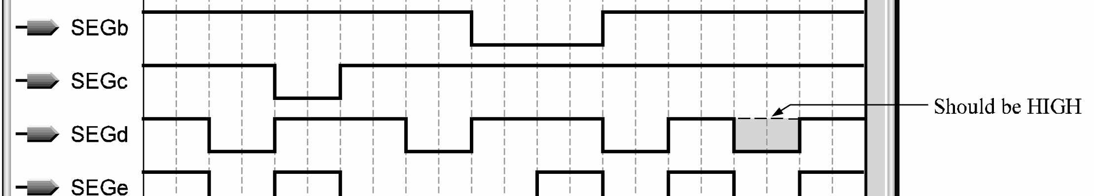
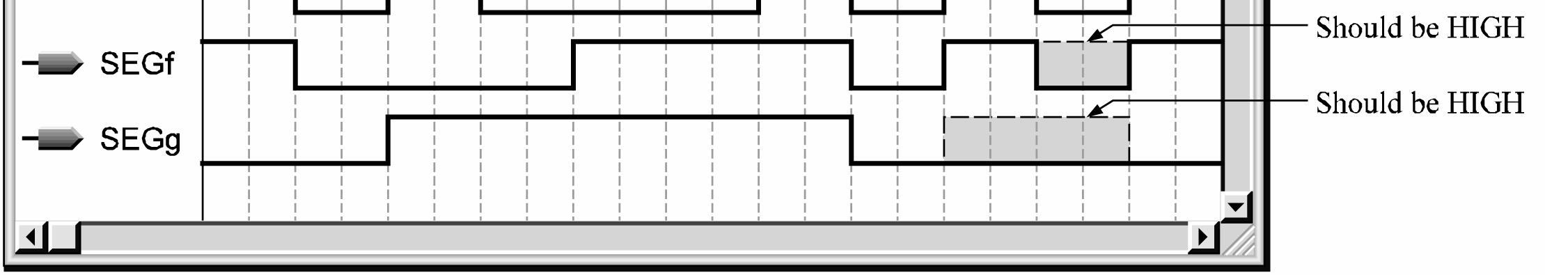
Section 12-1 Converting Analog Signals to Digital
1. See Figure 12-1.
2. See Figure 12-2.
3. 11, 11, 11, 11, 01, 11, 11, 11, 11
4. 1000, 1110, 1011, 0100, 0001, 0111, 1110, 1011, 0100
5. See Figure 12-3.
6. See Figure 12-4.
10. Number of comparators = 8 2121 n =− = 255
11. 001, 010, 011, 101, 110, 111, 111, 111, 111, 110, 101, 101, 110, 110, 110, 101, 100, 011, 010, 001.
See Figure 12-5.
12-5
12. Output of 3-bit converter: 000, 001, 100, 110, 101, 100, 011, 010, 001, 001, 011, 110, 111, 111, 111, 111, 111, 111, 111, 100.
See Figure 12-6.
12-6
14.
SAR Comment 11 11 11
Less than Vin. Keep the 1.
Less than Vin. Keep the 1. Less than Vin. Keep the 1.
Conversion never terminates since 2 bits cannot represent the input.
SAR Comment 1000 0100 0110
Greater than Vin. Reset MSB. Less than Vin. Keep the 1. Equal to Vin. Keep the 1 (final state)
15. See Figure 12-7.
16. R0 = 10 kΩ
R1 = 2 k 10 2 0 Ω = R = 5 kΩ
R2 = 4 k 10 4 0 Ω = R = 2.5 kΩ
R3 = 8 k 10 8 0 Ω = R = 1.25 kΩ
17. See Figure 12-8.
18. See Figure 12-9.
20. See Figure 12-10.
21. See Figure 12-11.
12-10
12-11
22. See Figure 12-12.
12-12
23. The purpose of analog-to-digital conversion is to change an analog signal into a sequence of digital codes that represent the amplitude of the analog signal with respect to time.
24. See Figure 12-13.
12-13
25. The purpose of digital-to-analog conversion is to change a sequence of digital codes into an analog signal represented by the digital codes.
26. 2000 MIPS × bits/byte 8 bit/instruction 32 = 2000 MIPS × 4 bytes/instruction = 8000 Mbytes/s
27. uctionbits/instr 32 Mbits/s 400 = 12.5 million instructions/s
28. 1000 MFLOPS = 1,000,000,000 floating-point operations/s
29. 1. Program address generate (PG). The program address is generated by the CPU.
2. Program address send (PS). The program address is sent to the memory.
3. Program access ready wait (PW). A memory read operation occurs.
4. Program fetch packet receive (PR). The CPU receives the packet of instructions.
30. 1. Instruction dispatch (DP): Instruction packets are split into execute packets and assigned to functional units;
2. Instruction decode (DC): Instructions are decoded.
1. The basic elements of a computer are central processing unit (CPU), memory unit, and input/output ports.
2. Two types of software are system and application.
3. A bus is a set of physical connections over which data and other information is transferred in a computer according to a standard set of specifications.
4. A port is a physical interface on a computer through which data is passed to and from peripherals.
5. The basic elements of a microprocessor are arithmetic logic unit (ALU), instruction decoder, control unit, and register array.
6. A microprocessor performs arithmetic operations, logic operations, data movements, and decision functions.
7. The three microprocessor buses are address, data, and control.
8. Groups of Pentium instructions are: data transfer, arithmetic and logic, bit manipulation, loops and jumps, strings, subroutines and interrupts, and control.
9. Pipelining is the process by which a microprocessor begins executing the next instruction before the previous instruction has been completed.
10. Multitasking is the process of executing more than one program at a time. Multithreading is the process of executing different parts (threads) of a single program simultaneously.
11. A microprocessor repeatedly cycles through fetch, decode, execute.
12 Pipelining is the process of fetching and executing at the same time so that more than one instruction can be processed simultaneously.
13. The six segment registers of the 80386 and above are: CS, DS, SS, ES, FS, GS
14. The code segment (CS) register contains 0F05 and the instruction pointer contains 0100. The physical address is
0F050 + 0100 = 0F150
15. AH and AL are 8-bit registers and represent the high and low part of the 16-bit AX register. The EAX is a 32-bit register which includes the AX register as the lower 16 bits.
16. (a) A flag is a bit stored in the flag register that is set or cleared by the processor. (b) A flag indicates a status or a control condition. A status flag is an indicator of a condition after an arithmetic or logic operation. A control flag alters processor operations under certain conditions.
17. Instruction pairing allows two instructions to execute at the same time.
18. An assembler is a program that translates mnemonics and operands into machine code.
19. The flowchart in Figure 13-1 shows the process for adding numbers from one to ten and saving the results in a memory location named TOTAL.
20. The flowchart in Figure 13-2 shows how you can count the number of bytes in a string and place the count in a memory location called COUNT. The string starts at a location named START and uses 20H (space) to indicate the end.
21. When the instruction mov ax, [bx] is executed, the word in memory pointed to by the bx register is copied to the ax register.
22. A compiler is a program that compiles or translates a program written in high-level language and converts it to machine code.
23. In a polled I/O, the CPU polls each device in turn to see if it needs service; in an interruptdriven system, the peripheral device signals the CPU when it requires service.
24. Vectoring is when the PIC provides a pointer to a service routine.
25. A software interrupt is a program instruction that invokes an interrupt service routine.
26. In a DMA operation, the DMA controller is given control by the CPU and allows data to flow between memory and a peripheral directly, bypassing the CPU.
27. The CPU is bypassed in DMA. FIGURE 13-2
28. See Figure 13-3.
13-3
29. See Figure 13-4.
13-4
30. See Figure 13-5.
13-5
31. The local bus is the collection of buses interfacing directly with the processor. The PCI bus is used for expansion devices and is connected to the local bus through a bus controller.
32. Plug-and-Play refers to self-configuring hardware that can be installed into and used in a computer system without the need for manual installation of jumpers or setting of switches.
33. The PCI bus is a 33 or 66 MHz, 32- or 64-bit, plug-and-play compatible expansion bus. ISA is an 8- or 16-bit 8.33 MHz expansion bus. PCI supports 3.3 V supplies while ISA supports 5 V and 12 V supplies.
34. A shorter RS-232C cable can support faster communication rates.
35. DCE stands for data communications equipment, such as a modem. DTE stands for data terminal equipment, such as a computer. Both acronyms are associated with the RS-232/EIA232 standard.
36. A USB cable consists of a power line, ground line, and two differential data lines.
37. Since there are eight instruments already on the bus and the limit is fourteen, six more instruments can be connected.
38. Three data bytes are transferred because the NDAC line goes HIGH three times, each time indicating that a data byte is accepted.
39. A controller is sending data to two listeners. The first two bytes of data (3F and 41) go to the listener with address 001A. The second two bytes go to the listener with address 001B. The handshake signals (DAV, NRFD, and NDAC) indicate that the data transfer is successful. See Figure 13-6.
40. If a talker sends a data byte to a listener on a GPIB system and a DTE sends a data byte to a DCE on an RS-232C system, the RS-232C system will receive the data first. This is because GPIB requires significantly more setup and handshaking than RS-232C.
1. No, because the VOH(min) is less than the VIH(min). The gate may interpret 2.2 V as a LOW.
2. Yes, they are compatible because the VOL(max) is less than the VIL(max)
3. VNH = VOH(min) VIH(min) = 2.4 V 2.25 V = 0.15 V
VNL = VIL(max) VOL(max) = 0.65 V 0.4 V = 0.25 V
4. The maximum amplitudes equal the noise margins of 0.15 V and 0.25 V.
5. Gate A: VNH = 2.4 V 2 V = 0.4 V VNL = 0.8 V 0.4 V = 0.4 V
Gate B: VNH = 3.5 V 2.5 V = 1 V VNL = 0.6 V 0.2 V = 0.4 V
Gate C: VNH = 4.2 V 3.2 V = 1 V VNL = 0.8 V 0.2 V = 0.6 V
Gate C has the highest noise margins.
6. PD(LOW) = (5 V)(2 mA) = 10 mW
PD(HIGH) = (5 V)(3.5 mA) = 17.5 mW PD(avg) = 2
7. The pulse goes through three gates in the shortest path. 3
9. Gate A average propagation
product = (1.1
ns 10 ns 10 + = 10 ns
Gate C average propagation delay: 2
Speed/Power product = (10 ns)(0.5 mW) = 5 pJ
Gate C has the best speed/power product.
10. Gate A can be operated at the highest frequency because it has the shortest propagation delay.
11. G2 is overloaded because it has 12 unit loads.
12. The network in (a) can operate at the highest frequency because the driving gate has fewer loads.
13. (a) ON (b) OFF (c) OFF (d) ON
14. Unused inputs should be connected as follows: Negative-OR gate (NAND) to VCC NAND gate to + VCC NOR gate to ground
15. See Figure 14-1 for another possible approach in addition to circuit given in text answers.
Selection inputs
FIGURE 14-1
16. (a) ON: high voltage on base forward-biases the base-emitter junction.
(b) OFF: insufficient voltage on base to forward-bias the base-emitter junction.
(c) OFF: emitter is more positive than the base which reverse-biases the base-emitter junction.
(d) OFF: base and emitter at same voltage. No forward bias.
17. See Figure 14-2.
14-2
18. Connect a 1 kΩ pull-up resistor to the unused inputs of the two NAND gates. Connect the unused input of the NOR gate to ground. Connect a pull-up resistor to the open collector of the NOR gate (value depends on load).
Section
19. See Figure 14-3.
14-3
20. (a) The driving gate output is HIGH, it is sourcing 3 unit loads.
IT = 3(40 μA) = 120 μA
(b) The driving gate output is LOW, it is sinking current from 2 unit loads.
IT = 2( 1.6 mA) = 3.2 mA
(c) G1 output is HIGH, it is sourcing 6 unit loads.
IT = 6(40 μA) = 240 μA
G2 output is LOW, it is sinking current from 2 unit loads.
IT = 2( 1.6 mA) = 3.2 mA
G3 output is HIGH, it is sourcing 2 unit loads.
IT = 2(40 μA) = 80 μA
21. See Figure 14-4. Pull-up resistors of second-level inverters are not shown.
14-4
22. (a) X = D ABC
(b) X = ) )( )( ( FG DE ABC
(c) X =
23. Worst case for determining minimum Rp is when only one gate is sinking all of the current (40 mA maximum).
For 10 UL: IL = 10(1.6 mA) = 16 mA For each gate: IRp(max) = IOL(max) 16 mA = 40 mA 16 mA = 24 mA
Rp(min) for (a), (b), and (c) is the same value.
24. See Figure 14-5.
14-5
25. F series: SPP = 3.3 ns × 6 mW = 19.8 pJ
LS series: SPP = 10 ns × 2.2 mW = 22 pJ
ALS series: SPP = 7 ns × 1.4 mW = 9.8 pJ
ABT series: SPP = 3.2 ns × 17 μW = 0.0544 pJ
HC series: SPP = 7 ns × 2.75 μW = 0.01925 pJ
AC series: SPP = 5 ns × 0.55 μW = 0.00275 pJ
AHC series: SPP = 3.7 ns × 2.75 μW = 0.010175 pJ
LV series: SPP = 9 ns × 1.6 μW = 0.0144 pJ
LVC series: SPP = 4.3 ns 0.8 μW = 0.00344 pJ
ALVC series: SPP = 3 ns × 0.8 μW = 0.0024 pJ
ALVC has the best (lowest value) speed-power product. It is, however, misleading to compare CMOS and TTL in terms of SPP because the power of CMOS goes up with frequency.
26. (a) ALVC (b) AHC (c) AC (d) ALVC
27. (a) A and B to X: 3(3.3 ns) = 9.9 ns
C and D to X: 2(3.3 ns) = 6.6 ns
(b) A to X1, X2, X3: 2(7 ns) = 14 ns
B to X1: 7 ns
C to X2: 7 ns
D to X3: 7 ns
(c) A, B to X: 3(3.7 ns) = 11.1 ns
C, D, to X: 2(3.7 ns) = 7.4 ns
28. (a) HC has an fmax = 50 MHz
fclock = ns 50 1 = 20 MHz
(b) LS has an fmax = 33 MHz
fclock = ns 60 1 = 16.7 MHz
(c) AHC has an fmax = 170 MHz
fclock = ns 4 1 = 250 MHz
Since fclock > fmax for the AHC flip-flop, the output will be erratic.
29. ECL operates with nonsaturated BJTs whereas TTL transistors saturate when turned on.
30. (a) Lowest propagation delay - ECL
(b) Lowest power – CMOS HC series
(c) Lowest speed/power product – CMOS HC series
1. The digit 2 is formed by segments a, b, d, e, g.
2. The digit 5 is formed by segments a, c, d, f, g.
3. The letter A is formed by segments a, b, c, e, f, g.
4. The letter E is formed by segments a, d, e, f, g
5. There is no segment common to all digits.
6. There is no segment common to all the letters shown in text Figure 4-46.
7. Segment d is used in letters b, C, d, and E. The hexadecimal code for each letter is as follows: b—1011; C—1100; d—1101; E—1100.
The expression for segment d is d = 3210321032103210 HHHHHHHHHHHHHHHH +++
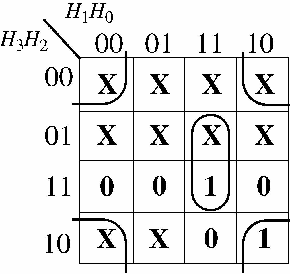
The minimized expression for segment d is d = 20210 HHHHH +
8. Segment e is used in letters A, b, C, d, and E. The hexadecimal code for each letter is as follows: A—1010; b—1011; C—1100; d—1101; E—1110.
The expression for segment e is e = 32103210321032103210 HHHHHHHHHHHHHHHHHHHH ++++
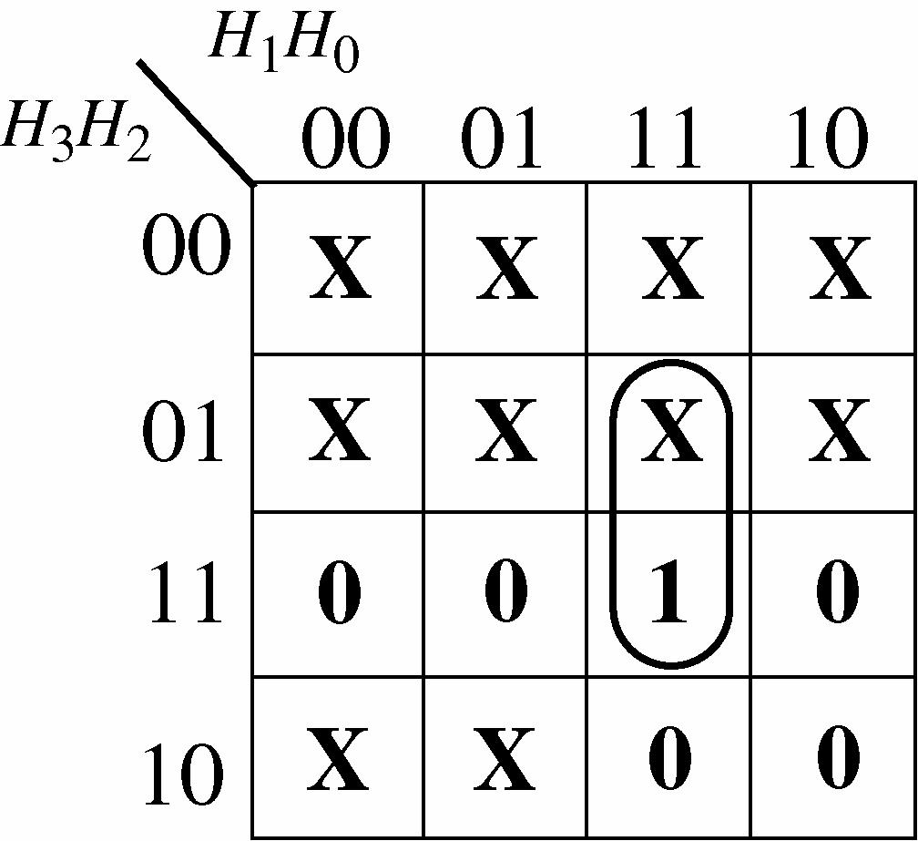
The minimized expression for segment e is
e = 210 H HH
9. Segment f is used in letters A, b, C, and E. The hexadecimal code for each letter is as follows: A—1010; b—1011; C—1100; E—1110.
The expression for segment f is
f = 3210321032103210 HHHHHHHHHHHHHHHH +++
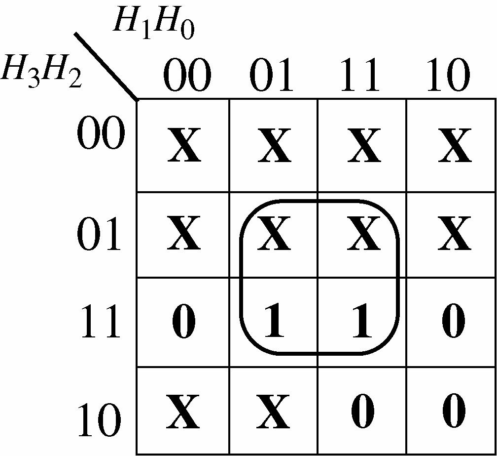
The minimized expression for segment f is f = 20 H H
10. Segment g is used in letters A, b, d, and E. The hexadecimal code for each letter is as follows: A—1010; b—1011; d—1101; E—1110.
The expression for segment g is
g = 3210321032103210 HHHHHHHHHHHHHHHH +++
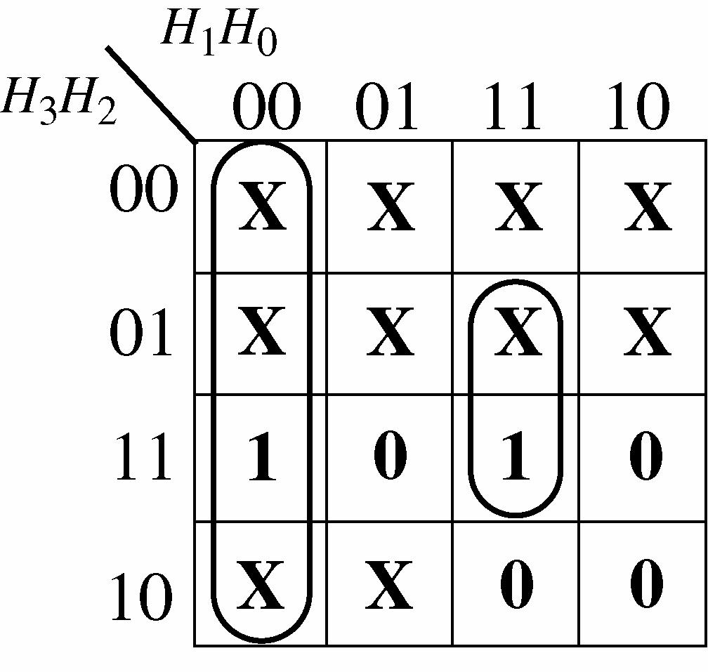
The minimized expression for segment g is
11. The location for segment d is
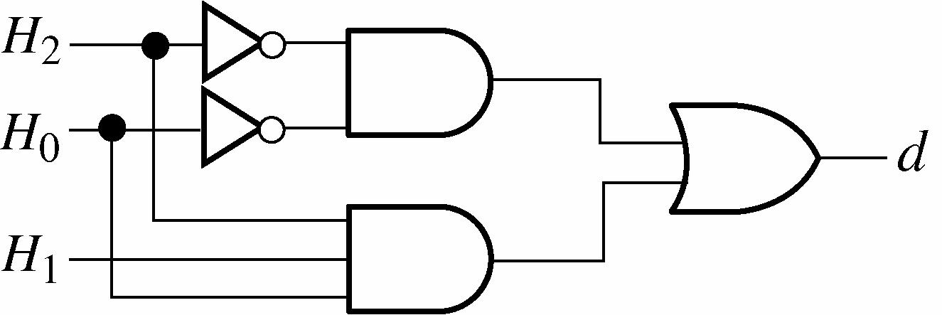
12. The logic for segment e is
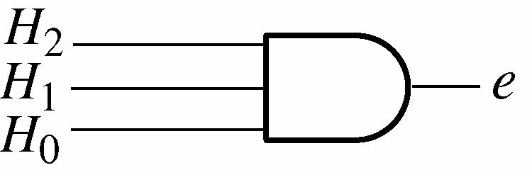
13. The logic for segment f is
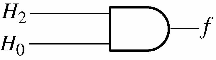
14. The logic for segment g is
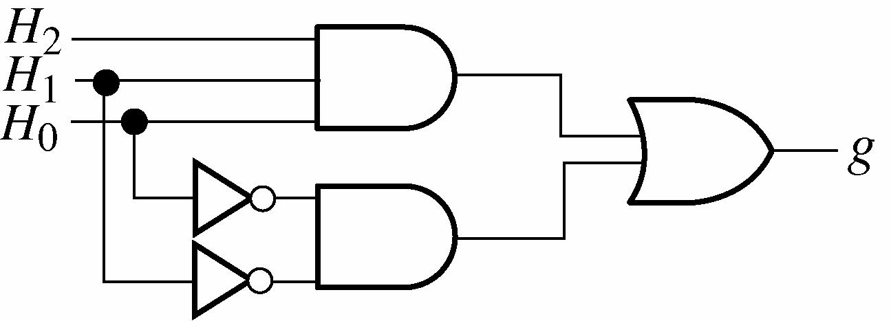
Putting Your Knowledge to Work
To modify the decoder for a common-cathode display, the segment outputs must be active-HIGH. An inverter in each segment output will provide an active-HIGH.
1. The two “cannot occur” conditions in text Table 5-6 are not possible because if the maximum level, LMAX, has been reached as indicated by a 1, the minimum level LMIN also must have been reached, but the 0 indicates that it has not.
2. The inlet valve is open under three conditions as indicated by VINLET = 1.
3. The inlet valve turns off when the maximum level is reached.
4. The standard SOP expression for Vinlet is
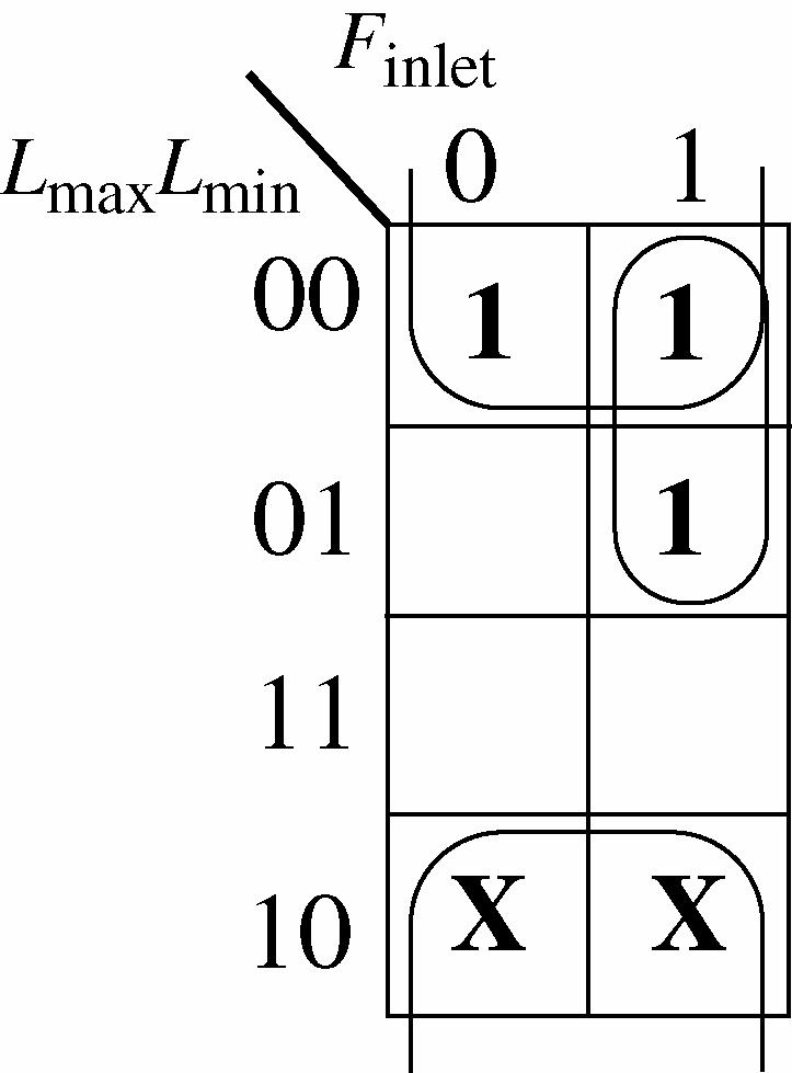
The simplified Vinlet expression is correct.
inlet = minL + maxinletLF
5. The simplified logic for the inlet valve control:
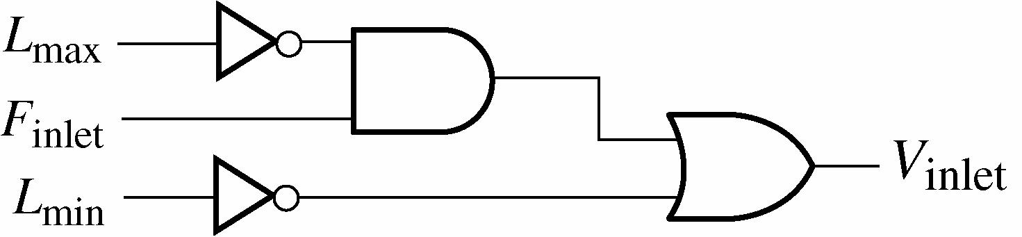
6. The additional input to the outlet valve control is T for temperature. The corn syrup must be at a specified temperature for proper viscosity before the syrup can be released into the mixing vat.
7. The outlet valve is open under two conditions as specified by the 1s in text Table 5-7.
8. Once the tank starts draining, the outlet value remains open (on) until the minimum level is reached.
9. The standard SOP expression for Voutlet is
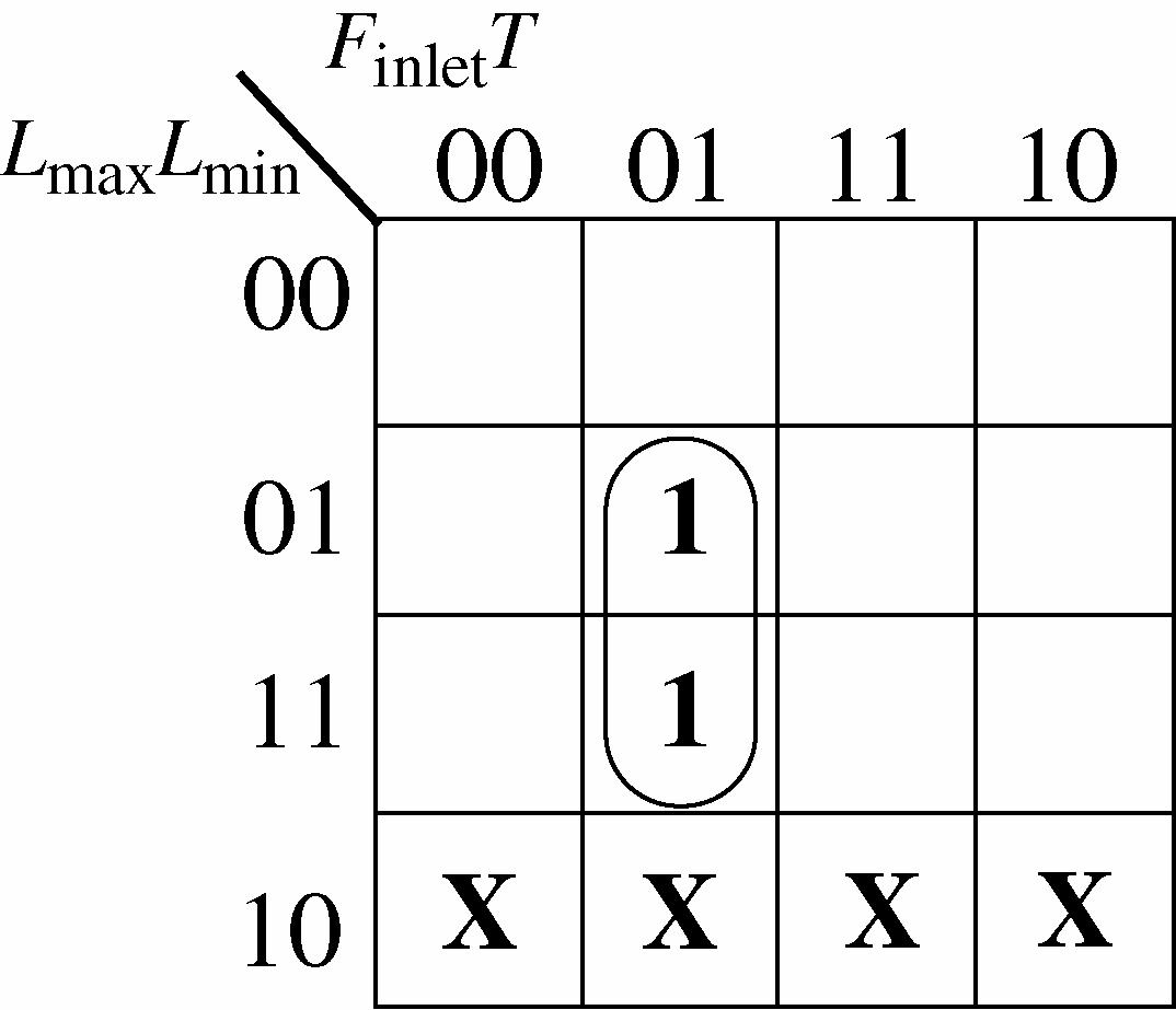
The simplified Voutlet expression is correct.
Voutlet = mininlet LFT
10. The simplified logic for the outlet valve control:
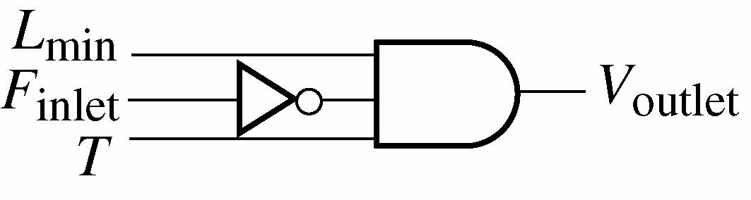
Putting Your Knowledge to Work
This assumes that the corn syrup is acceptable as long as its temperature is no more than 9° below the specified temperature. The temperature control circuit could be modified by eliminating the LSD in the BCD code for the measured temperature.
1. The system remains in the first state (00) for 25 s if there is a vehicle on the side street or as long as there is no vehicle on the side street.
2. The system remains in the fourth state (10) for 4 s.
3. The expression for the condition producing a transition from the first state to the second state is
4. The expression for the condition that keeps the system in the second state is
5. The diagram for the light output logic:
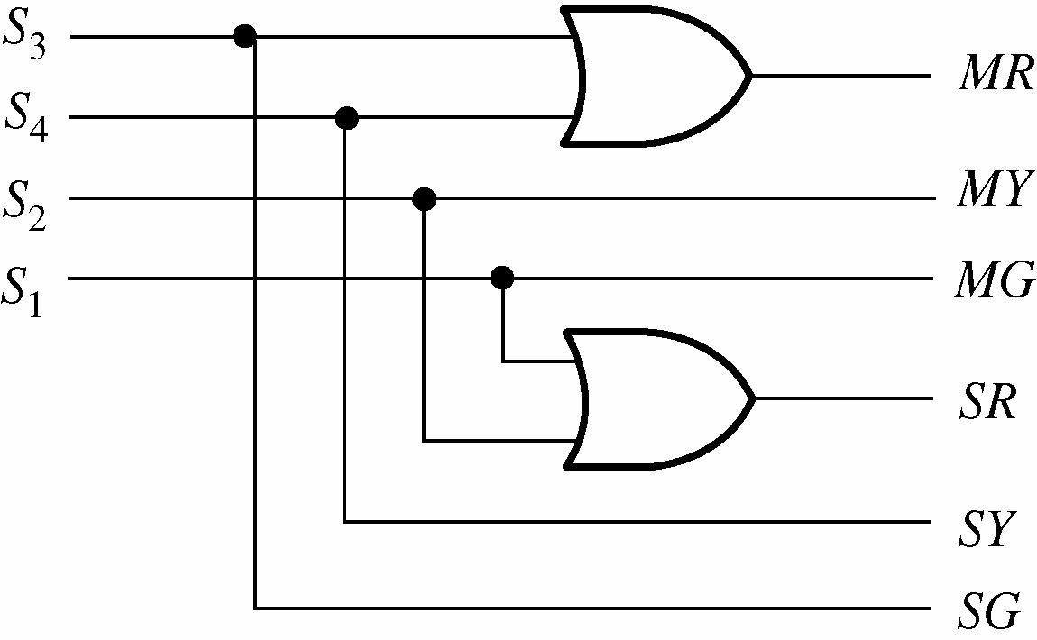
6. The truth table for the light output logic:
7. The diagram for the trigger logic:
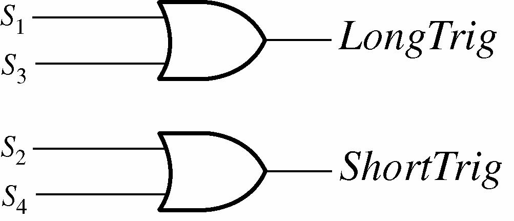
8. The truth table for the trigger logic:
9. The diagram of the complete combinational logic:
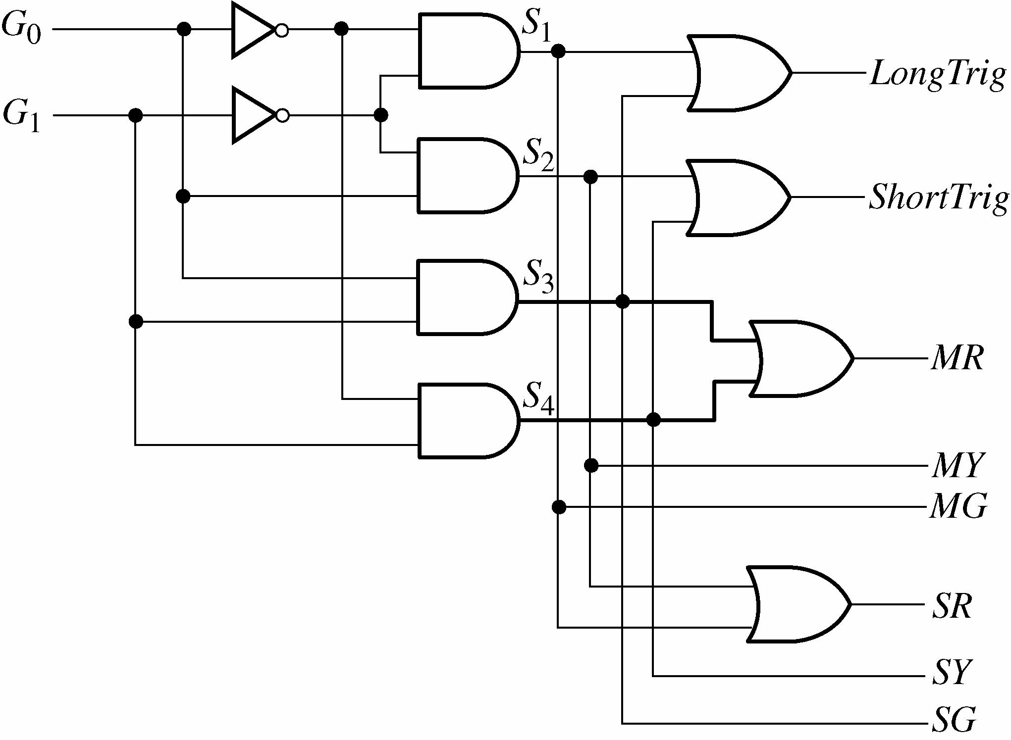
(a) One approach is shown by the modified state diagram.
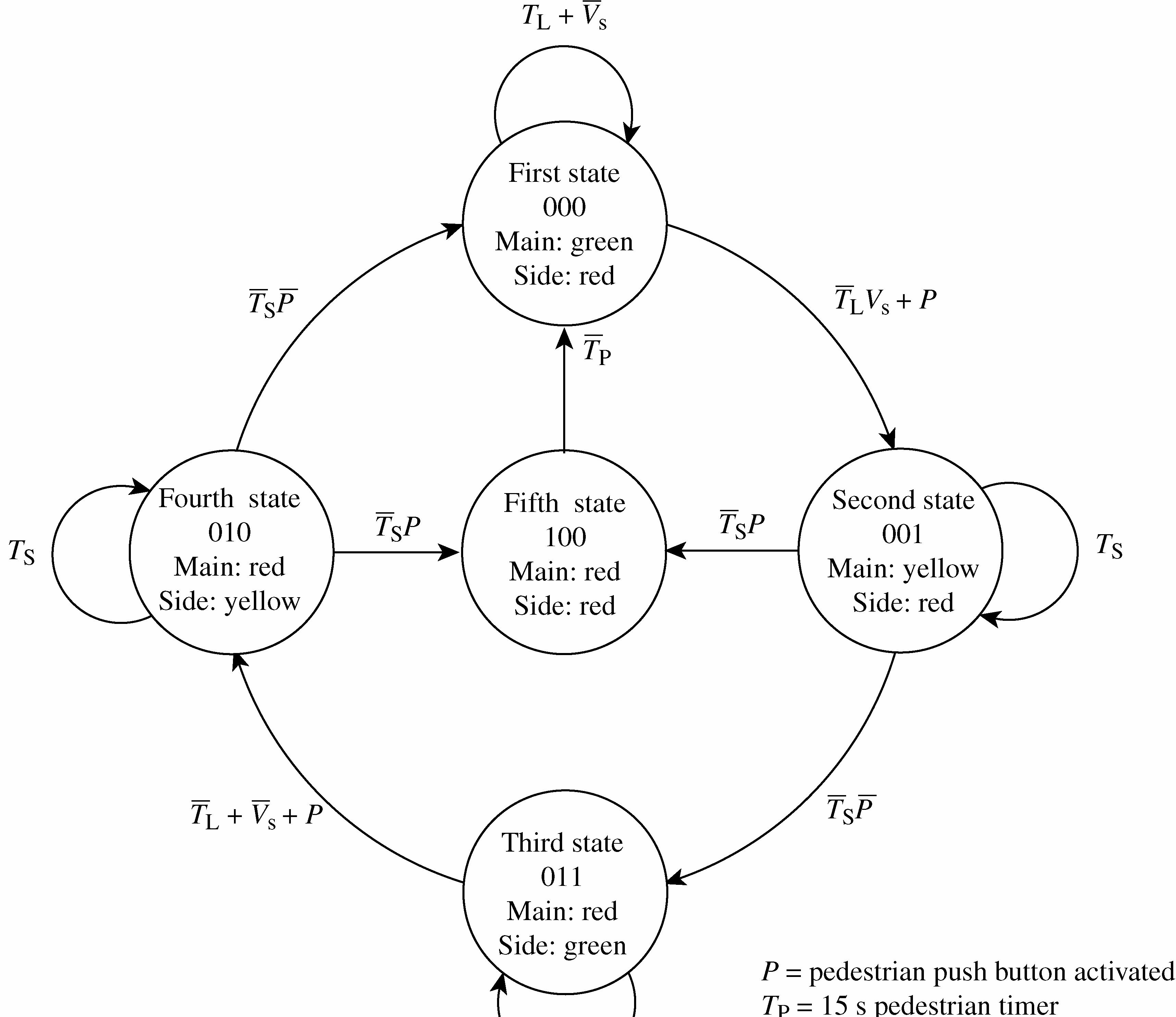
When a pedestrain pushes the button, one of the following sequences occurs:
If system is in first state (000), it goes immediately to second state (001) for 4 s and then to fifth state (100) for 15 s and then back to first state (000).
If system is in third state (011), it goes immediately to fourth state (010) for 4 s and then to fifth state (100) for 15 s and then back to first state (000).
If system is in either second or fourth states, the short timer is retriggerd and the system remains in that state for another 4 s before going to the fifth state.
(b) The modified combinational logic block diagram:
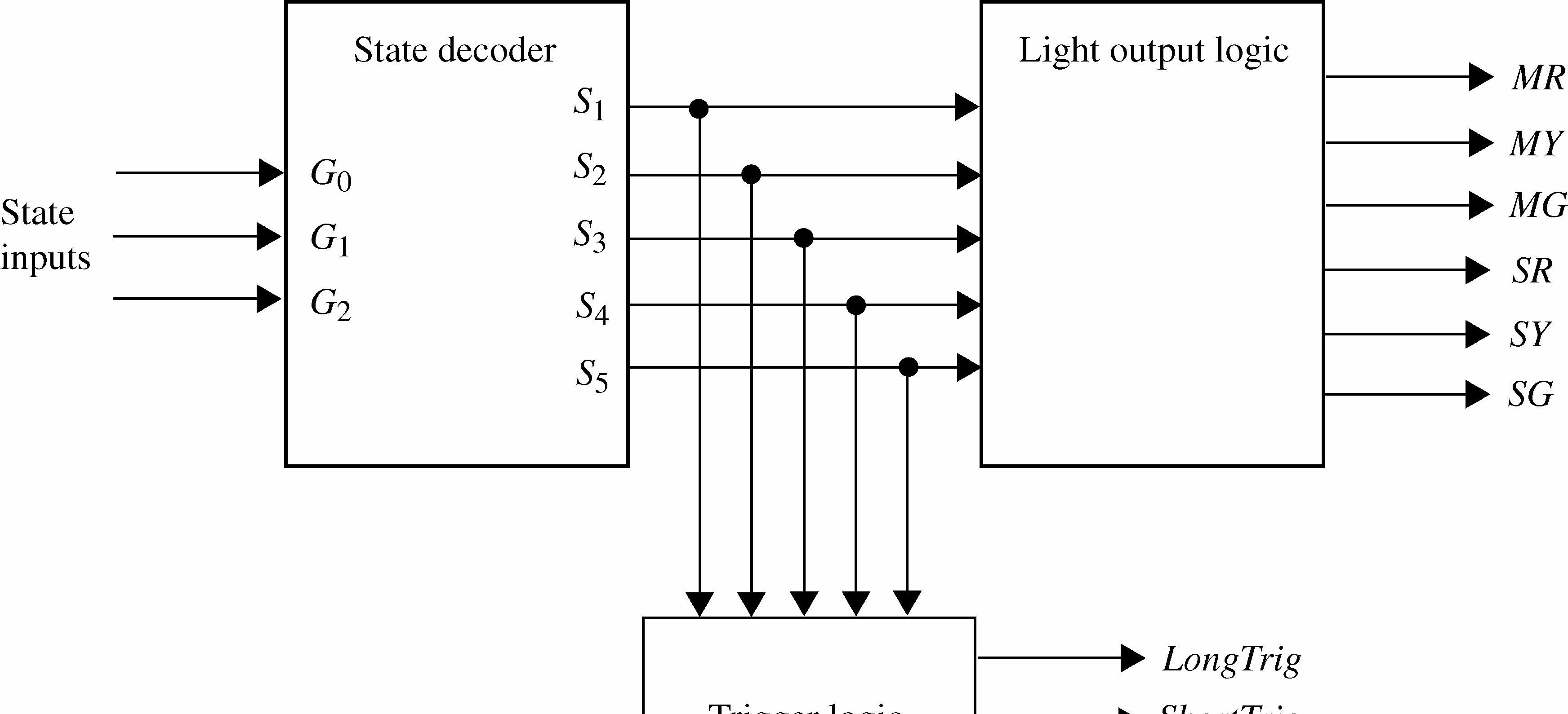
The modified state decoder logic:
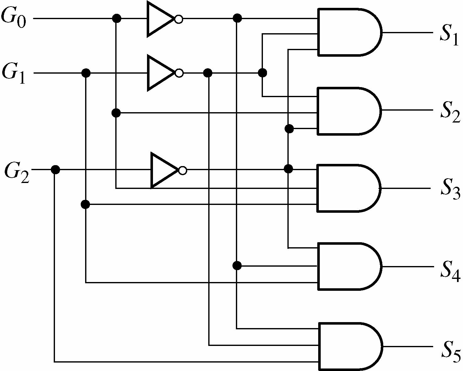
The modified light output logic:
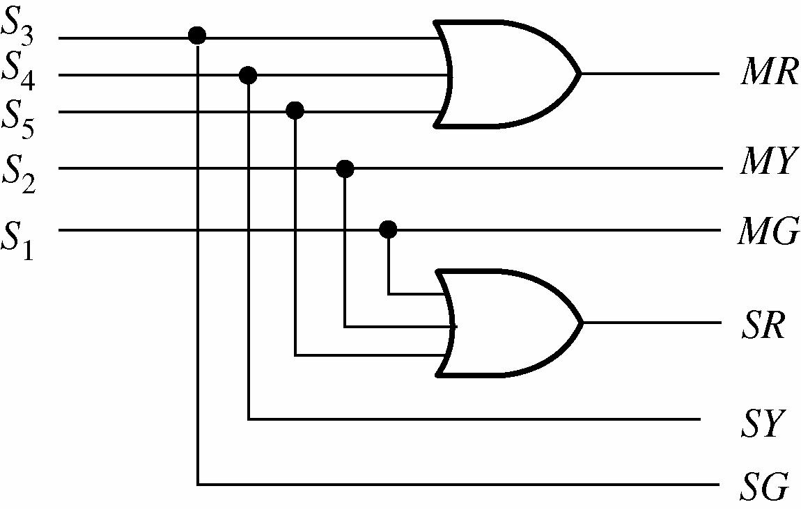
The modified trigger logic:
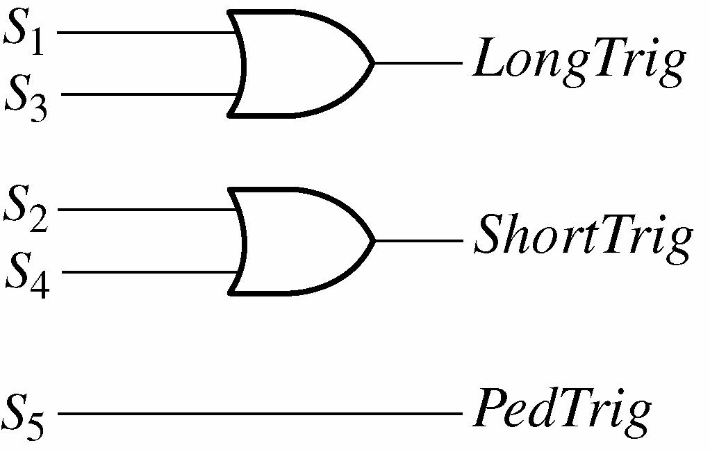
1. The resistor and capacitor values for the 25 s timer are determined as follows.
Let C1 = 100 μF
tW = 1.1R1C1
R1 = 1 25 s 1.11.1(100 μF) tW C = ≅ 227 kΩ
Other combinations are possible.
2. The resistor and capacitor values for the 4 s timer are determined as follows.
Let C1 = 100 μF
tW = 1.1R1C1
R1 = 4 s 1.1(100 μF) = 36.4 kΩ
Other combinations are possible.
3. The resistor and capacitor values for the 10 kHz oscillator are determined as follows.
Let C1 = 0.01 μF f = 121 1.44 (2) R RC +
R1 + 2R2 = 1 1.441.44 (10 kHz)(0.01 μF) fC = = 14.4 kΩ
Let R1 = 1.5 kΩ R2 = 14.4 k1.5
4. The 25 s timer and the 4 s timer using 74121 one-shots:
tW = 25 s; let CEXT = 10 μF
tW = 0.7REXTCEXT
REXT = EXT 25 s 0.70.7(10 μF) tW C = = 3.6 MΩ
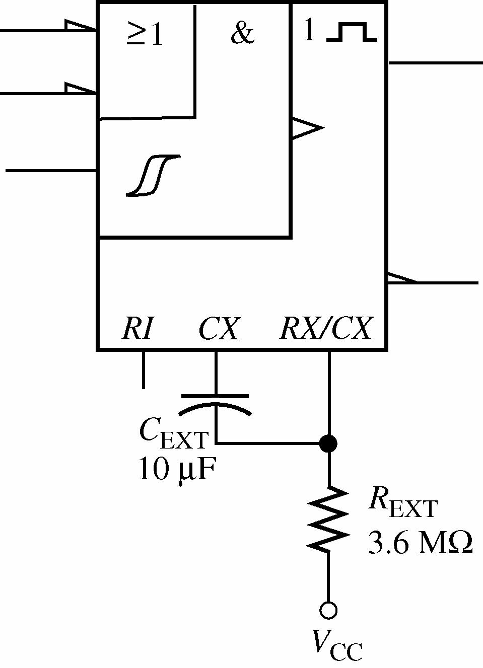
tW = 4 s; let CEXT = 10 μF
tW = 0.7REXTCEXT
REXT = 4 s 0.7(10 μF) = 571 kΩ
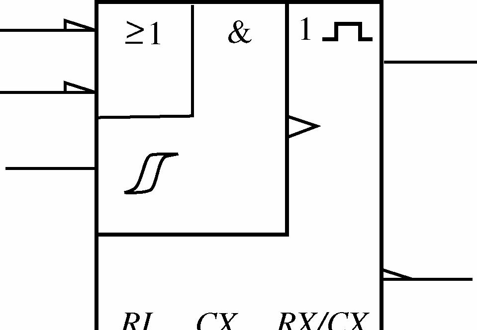
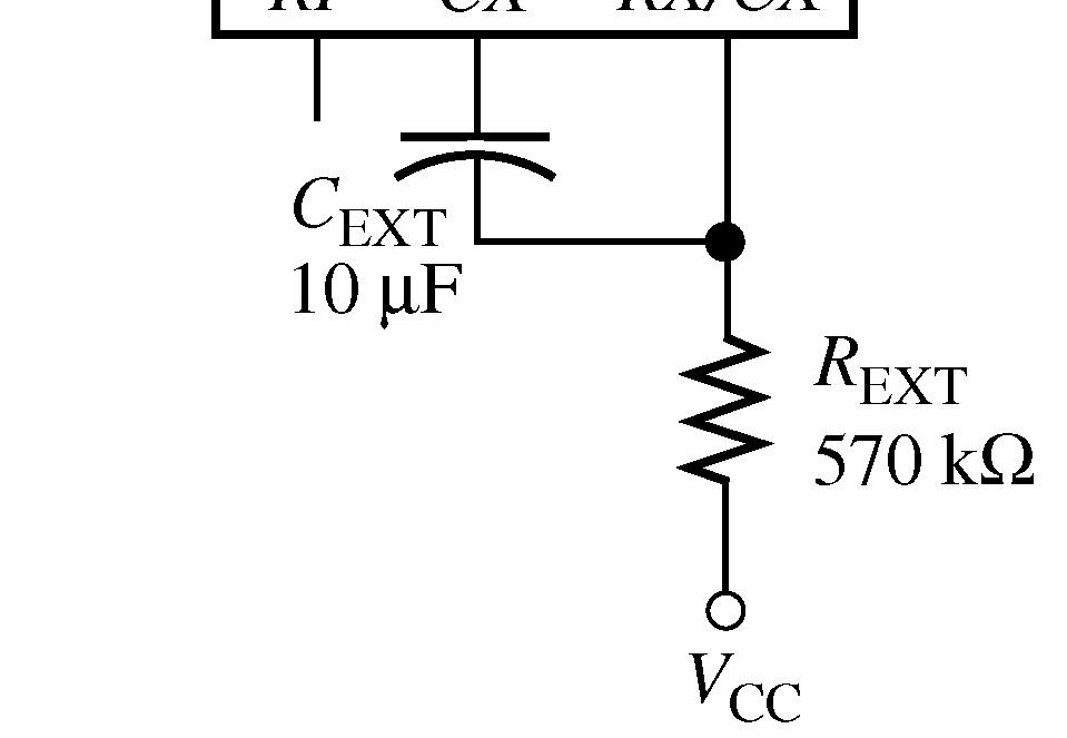
Real time is determined by connecting a Multisim probe to the one-shot output and measuring its ontime. Simulation time is determined by connecting a virtual oscilloscope to the one-shot output and measuring the pulse-width.
1. The Boolean rule used is 1 A A += .
In this case, the terms 10GG were factored out leaving SSTT + : 10SS1010 ()(1) GGTTGGGG +==
2. 0D is reduced by first expanding to standard SOP form:
010Ls1010LsD GGTVGGGGTV =++
= 10Ls10Ls10Ls10Ls10Ls10Ls GGTVGGTVGGTVGGTVGGTVGGTV +++++
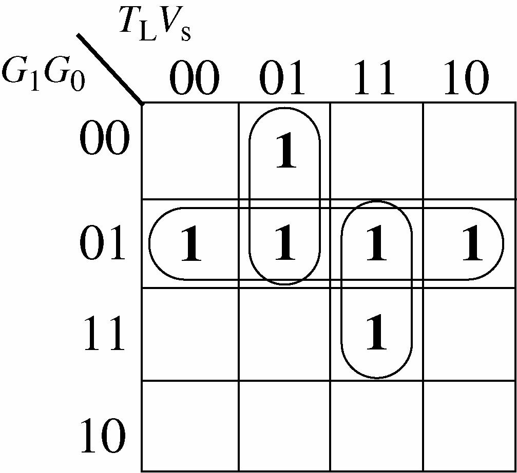
The reduced expression is
0101Ls0LsD GGGTVGTV=++
3. 1D has five variables and is reduced by applying Boolean rules:
GGTGGTVTGGVGGT =++++ =++++
110S10Ls10L10s10S
10S10LL10s10S s D GGTGGTVGGTGGVGGT
Applying the rule 11: AABAB +=+ ( )
110S10sL1010S s D GGTGGVTGGVGGT =++++
110S10s10L1010S 10S10sL10S s s D GGTGGVGGTGGVGGT GGTGGVTVGGT =++++ =++++
Applying the rules 2 and 6: 11 A + = and 1 AA + =
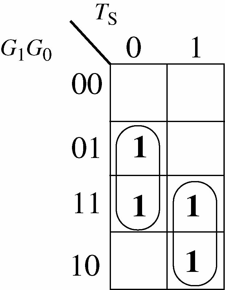
The reduced expression is
4. The expressions agree with text Figure 8-64.
Putting Your Knowledge to Work
The combinational logic portion of the system was modified in Chapter 6 to accommodate a pedestrian input to turn both lights red for 15 s. To accomplish this exercise, the student must recognize that the timing circuits and the sequential logic must also be modified.
Timing circuit modification: An additional 555 timer configured as a one-shot with a 15 s output pulse is addded:
Let C1 = 100 μF.
tW = 1.1R1C1 R1 = 15 s 1.1(100 F)μ = 136 kΩ
Sequential logic modification: A third flip-flop is added. First, the next-state table is modified to accommodate the pedestrian input (P).
DGGGTVPGGGTGGGTPGGGTV
0210Ls210S210S210Ls
GGGTVGGGPGGGTGGGTPGGGTV
210Ls210210S210S210Ls
DGGGTPGGGTVGGGTVPGGGT GGGTPGGGTVGGGTGGGVGGGPGGGT =+++++
1210S210Ls210Ls210S
210S210Ls210L210s210210S
2210S210SD GGGTPGGGTP=+
Notice that the expressions contain up to seven variables. Karnaugh map simplification would not be feasible. If you wish to minimize the expressions, the Quine-McCluskey method can be used but will be left as an exercise that can be assigned to students.
0D will take three 5-input AND (or NAND) gates, two 4-input AND (or NAND) gates, and one 5-input OR (or NAND) gate.
1D will take two 5-input AND (or NAND) gates, four 4-input AND (or NAND) gates, and one 6-input OR (or NAND).
2D will take two 5-input AND (or NAND) gates and one 2-input OR (or NAND) gate.
1. The BCD code sequence for 4739 is 0100, 0111, 0011, 1001.
2. The state of shift register C after two correct code digits are entered is 00000100.
3. The purpose of the OR gate is to produce a trigger when a key is pressed in order to generate the clock pulses for the system.
4. When the digit 4 is entered, 0100 appears on the outputs of register A.
The security code logic can be modified for a 5-digit code by moving the HIGH parallel input of shift register C back one position. It would then take five clock pulses to shift the 1 to the output.
1. The shift register initial outputs are 0 1, Q = 1 0 Q = , 2 0 Q = , 3 0 Q = .
2. The state of the shift register after three clock pulses is
3. The purpose of the OR gates is to produce the BCD code from the selected AND gates.
4. In text Figure 10-73, NAND gates are used to implement the AND-OR logic of Figure 10-72.
5. The resistor packs provide pull-up resistors for the DIP switch outputs.
The memory and code selection logic can be modified for a 5-bit code by adding a DIP switch with resistor pull-ups, four more AND gates, changing the OR gates to five inputs, and changing the shift register from four bits to five bits.
1. The logic expression for SEGa is SEGa = ACACBD + ++
The conditions for SEGa to be HIGH are indicated on the waveform in the following figure, showing that the waveform is correct.
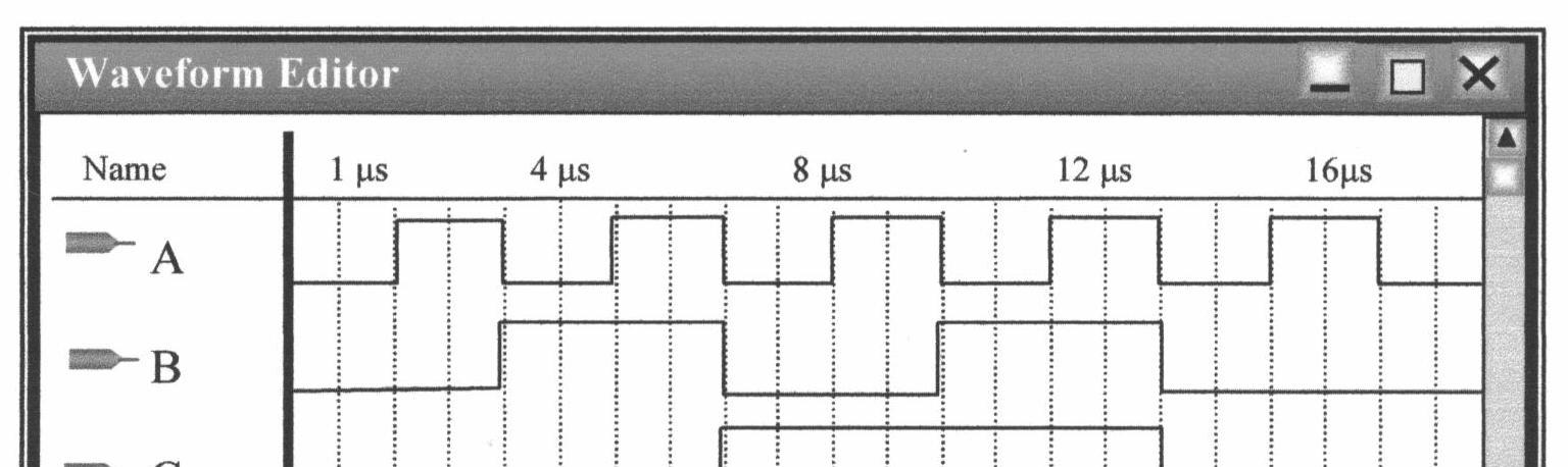
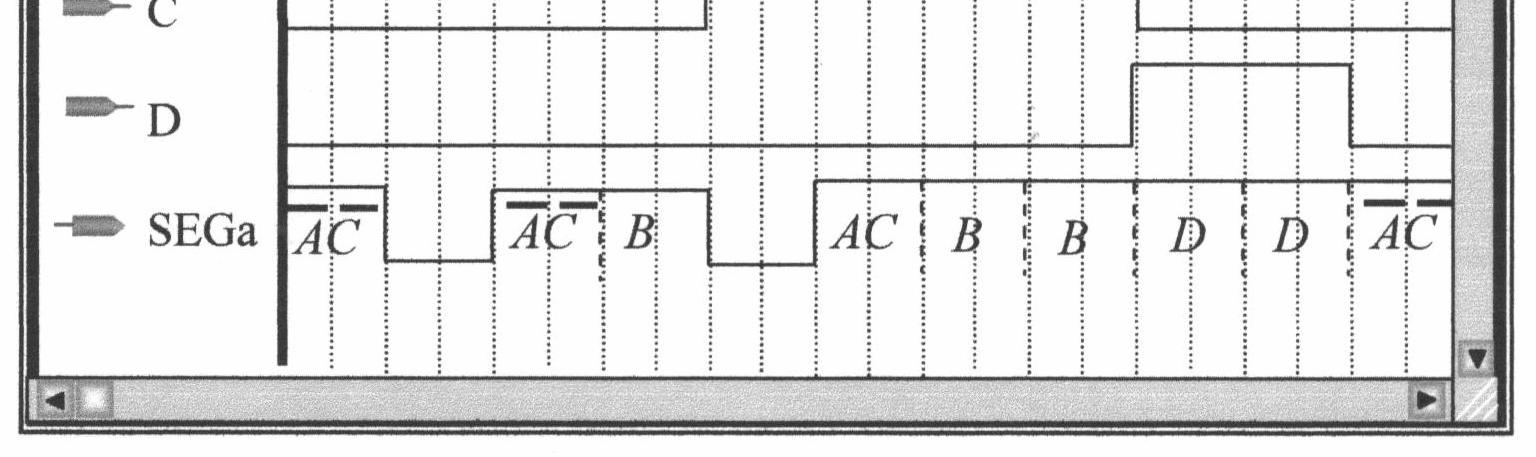
2. The logic expression for SEGb is SEGb = ABABC + +
The conditions for SEGb to be HIGH are indicated on the waveform in the following figure, showing that the waveform is correct.
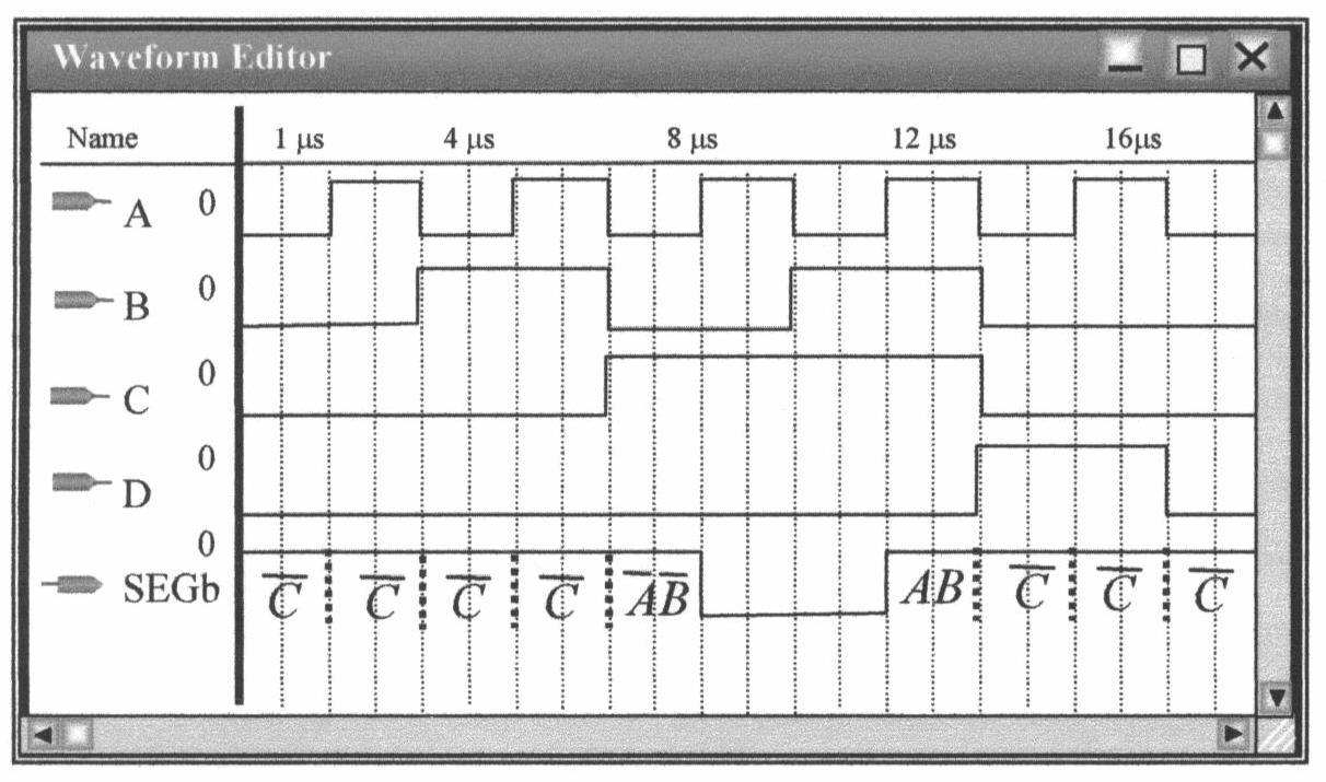
The logic expression for SEGc is SEGc = . ABC + +
The conditions for SEGc to be HIGH are indicated on the waveform in the following figure showing that the waveform is correct.
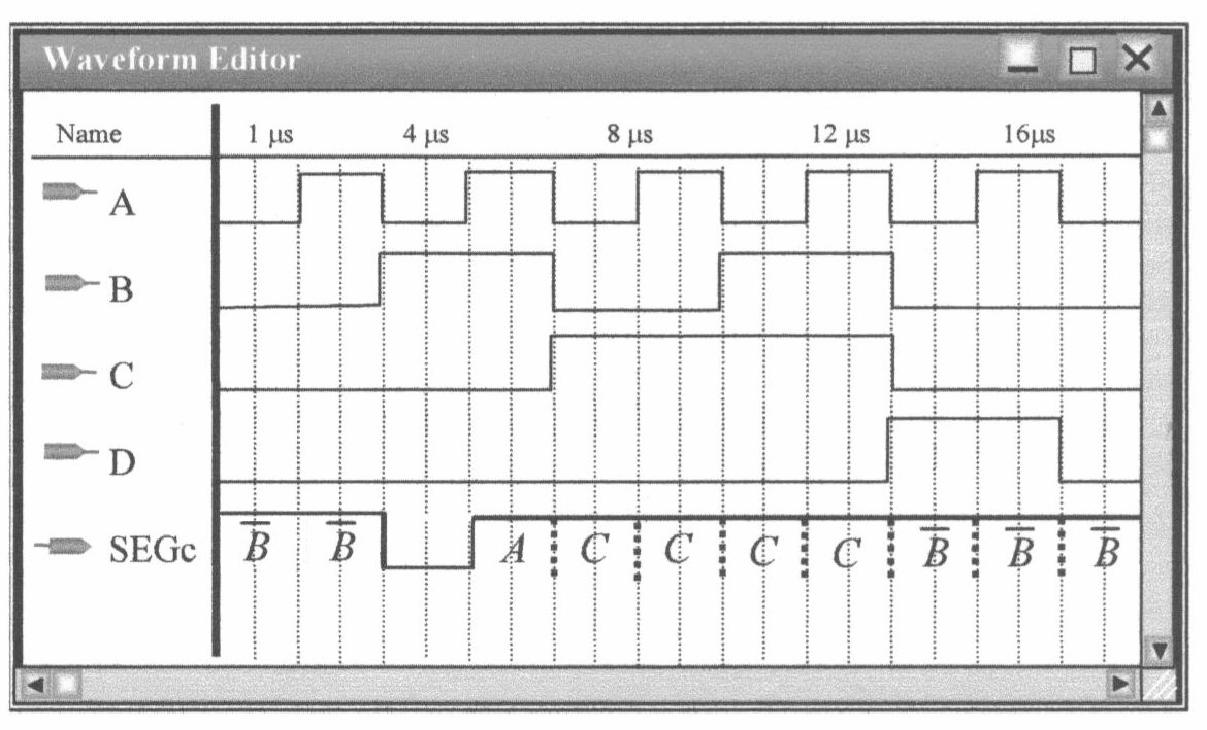
The logic expression for SEGd is SEGd = .ABACBCABCD + +++
The conditions for SEGd to be HIGH are indicated on the waveform in the following figure, showing that the waveform is correct.
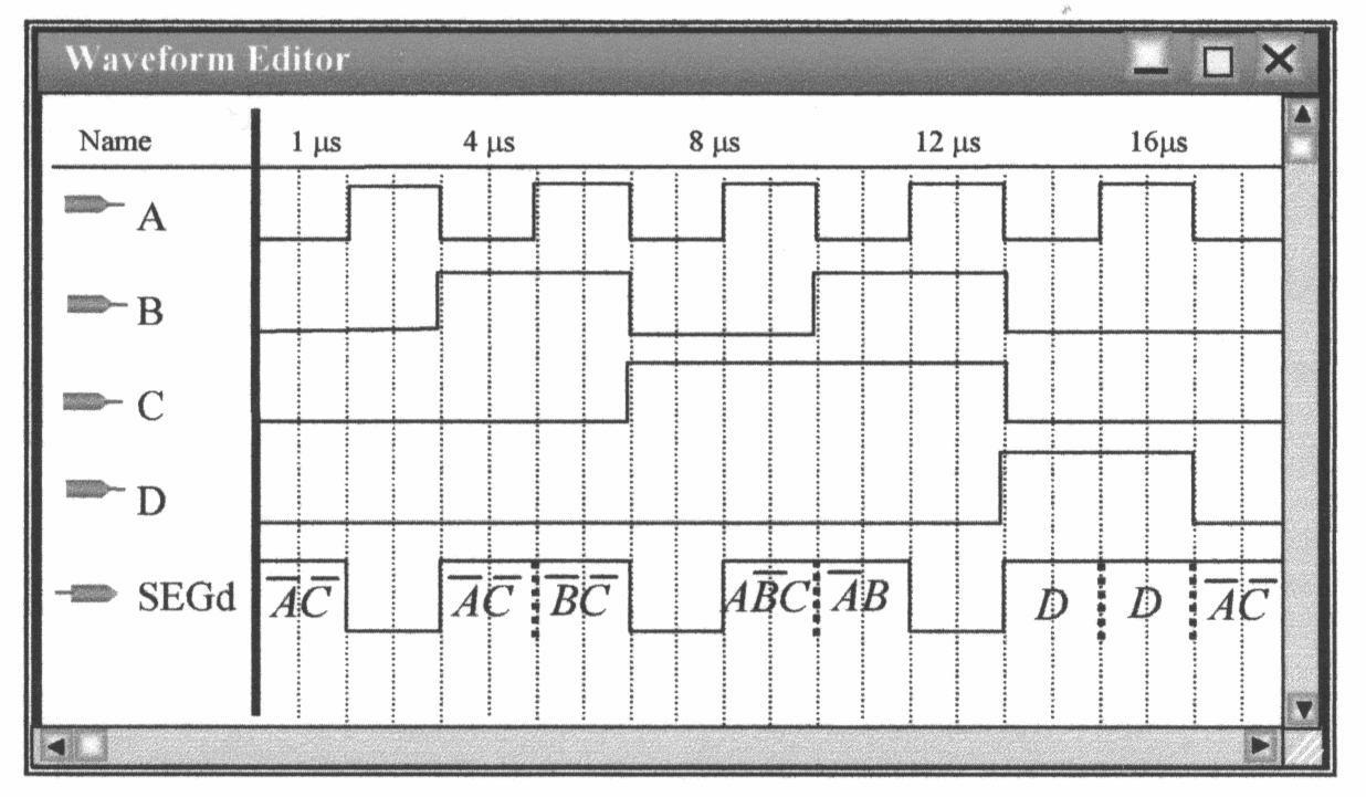
3. The logic expression for SEGe is SEGe = ABAC +
The waveform for SEGe is shown in the following figure.
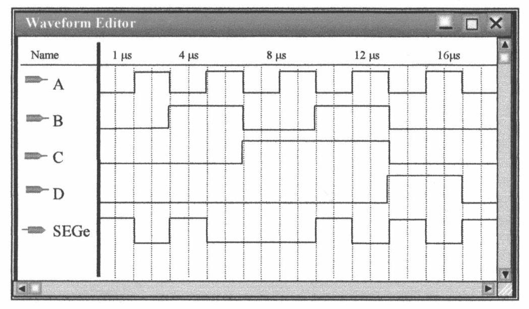
The logic expression for SEGf is SEGf = ABACBCD + ++
The waveform for SEGf is shown in the following figure.
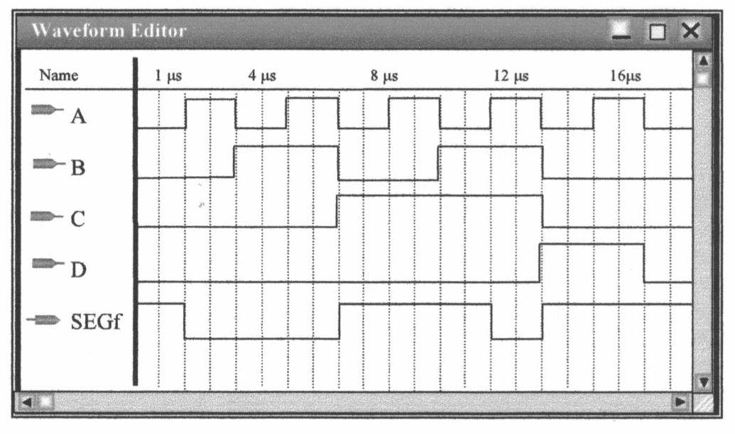
The logic expression for SEGg is SEGg = ABBCBCD + ++
The waveform for SEGg is shown in the following figure.
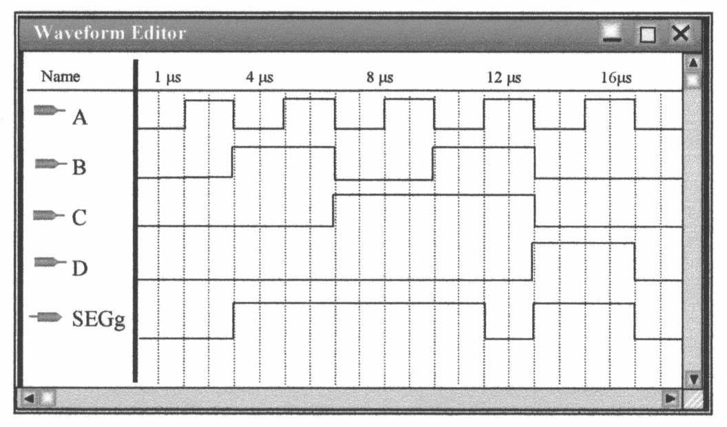
Explanation of Logic Symbols
Courtesy of Texas Instruments

David Buchla
Instructor Multisim Solutions ......267
Experiment 1:
Experiment 2:
Experiment 3:
Experiment 4:
Experiment 5:
Experiment 6:
Experiment 7:
Experiment 8:
Experiment 9:
Experiment 10:
Experiment 11:
Experiment 12:
Experiment 13:
Experiment 14:
Experiment 15:
Experiment 16:
Experiment 17:
Experiment 18:
Experiment 19:
Experiment 20:
Experiment 21:
Experiment 22:
Experiment 23:
Experiment 24:
Experiment 25:
Experiment 26:
Experiment 27:
Experiment 28:
Experiment 29:
Laboratory Instrument Familiarization.....269
Constructing a Logic Probe..... 271
Number Systems..... 272
Logic Gates.....274
More Logic Gates.....276
Interpreting Manufacturer’s Data Sheets.....278
Boolean Laws and DeMorgan's Theorems.....281
Logic Circuit Simplification.....284
The Perfect Pencil Machine.....287
The Molasses Tank.....289
Adder and Magnitude Comparator.....290
Combinational Logic Using Multiplexers.....291
Combinational Logic Using Demultiplexers.....293
The D Latch and D Flip-Flop.....295
The Fallen Carton Detector.....296
The J-K Flip-Flop.....297
One Shots and Astable Multivibrators.....298
Asynchronous Counters.....299
Analysis of Synchronous Counters with Decoding.....301
Design of Synchronous Counters.....303
The Traffic Signal Controller.....305
Shift Register Counters.....307
Application of Shift Register Circuits.....309
The Baseball Scoreboard.....311
Semiconductor Memories.....312
Introduction to Quartus II Software...313
D/A and A/D Conversion......314
Introduction to the Intel Processors.....315
Applications of Bus Systems....317
There are Multisim files for Multisim 9 and Multisim 10 files for seven experiments (5, 8, 10, 12, 18, 19, and 23) on the companion website. To access supplementary materials online, instructors need to request an instructor access code. Go to www.pearsonhighered.com/irc, where you can register for an instructor access code. Within 48 hours after registering, you will receive a confirming e-mail, including an instructor access code. Once you have received your code, go to the site and log on for full instructions on downloading the materials you wish to use.
The Multisim suffix is .ms9 (version 9) or .ms10 (version 10). The naming convention for all files is Exp-xxnf for files with no fault (“xx” refers to the experiment number). The “nf” in the file name is replaced with f1 and f2 for files with hidden faults. The circuit restrictions password that will allow faults to be revealed is df10lm for both Multisim versions. The circuit and fault descriptions are as follows:
File name Description
Exp-05nf
Exp-05f1
Exp-05f2
***********
Exp-08nf
Exp-08f1
Exp-08f2
***********
Exp-10nf
Exp-10f1
Exp-10f2
***********
Exp-12nf
Exp-12f1
Exp-12f2
***********
Exp-18nf
Exp-18f1
Exp-18f2
The circuit is from Figure 5-2 and performs either a 1’s or 2’s complement depending on the position of the “Complement” switch.
The 330 Ω resistor on the output of D1 is open.
The Complement switch is shorted.
***********
The circuit is the combinational logic circuit given in Figure 8-4, the BCD invalid code detector.
The input from the D switch to NAND2 is open at the NAND gate.
Switch C is shorted.
***********
The circuit is a simulation of the outlet valve for the model-1 Molasses tank given in Figure 10-2. To simulate the operation, open the LL switch (tank is filling), then open the LH switch (tank full). Close the LH switch and note that the valve remains open until LL is closed.
Resistor R3 is 3.3 kΩ (value not shown).
NAND gate U2B has an open output.
***********
The circuit is an overflow detection circuit, given as a design problem using gates in Experiment 11. A 74153 MUX is used in this problem.
The inverter has an open input.
The inverter has an input to output short.
***********
The circuit is counter shown in Figure 18-6 with an oscilloscope. Glitches are easily seen in Multisim, but they are more difficult to see in lab.
The CLK input to the FFB is open.
The Q output of FFA is open.
Exp-19nf
Exp-19f1
Exp-19f2
Exp-23nf
Exp-23f1
Exp-23f2
The circuit is the J-K counter in Figure 19-3 with no faults. The logic analyzer is used in place of LEDs on the output.
The preset switch is shorted to ground.
The third NAND gate from the top has an open output.
The circuit is the J-K counter in Figure 19-3 with no faults. The logic analyzer is used in place of LEDs on the output.
The start bit flip-flop has an open on the CLR input.
The inverter has an open output.
Data and Observations
Data and the number of significant figures will vary according to signal generator and measurement equipment. Sample (measured) data is shown.
TABLE 1-1
TABLE 1-2
= 5.0 V
TABLE 1-3
With the partial failure consisting of a 100 Ω resistor in parallel with the LED, most of the current goes through the resistor (Figure 1-8b). This current can be traced through R1 and R2 and back to the supply using a logic pulser and current tracer as shown in Figure 1-9. With the short circuit (Figure 1-10), the current can be traced along the protoboard’s bus, through the short and back to the supply with no current in the resistors or the LED.
1. The circuit can be damaged if the wrong voltage is connected to it.
2. Vertical section: sets the amplitude of the input signal and develops voltages for display section; it sends signals to the trigger section.
Trigger section: causes the start of the acquisition of the waveform. A stable display requires the trigger to occur at the same point on the waveform for each acquisition.
Horizontal section: controls the time base.
Display section: changes the intensity or other display parameters.
3. A probe from each channel is connected across the ungrounded component. All grounds are connected to the circuit ground. The scope is configured to measure the difference between the two channels. (This will vary between scope types; it sometimes requires the channels to be added with one channel inverted).
4. (a) The oscillator works but the LED is off. The voltage at pin 3 and the LED are identical. (b) The oscillator works but the frequency is too low (depending on the capacitor).
(c) Reversing the power and ground leads will result in destructively high current.
(d) The oscillator works but the LED is off. No voltage appears at the LED (but pin 3 is okay).
5. A digital oscilloscope is typically as accurate as a DMM and allows detection of noise or ripple with a power supply. A DMM is typically more portable. An analog scope is not as accurate as a DMM but does not show potential problems such as noise or ripple. A digital scope may be as accurate as a DMM because of automated measurement capability and gives more information than a DMM about potential problems such as the presence of noise.
6. Pulses from the logic pulser are applied to the circuit board trace that normally carries power but with power removed. The current tracer can be moved along this line, following the path of current until the short is found. (Note that this technique can be used for any board, analog or digital).
Data and Observations
TABLE 2-1
TABLE 2-2
Further Investigation Results:
The signals are nearly identical as shown. In the experimental circuit, a slight difference in amplitude was noted and the output is delayed by 14 ns on the leading edge and 16 ns on the trailing edge. The time difference is due to transition time through the gates.
Plot 1
Evaluation and Review Questions:
1. Increase the value of the 330 Ω resistor in the input voltage divider.
2. Two inverters in series form a buffer that can allow additional drive current from the same logic output.
3. (a) The circuits are identical.
(b) If the input to the first inverter is open, an invalid level of approximately 1.6 V will be observed.
(c) If the input to the first inverter is open, then the output will be LOW.
4. A logic probe can quickly determine if a valid logic HIGH or LOW is present at some point in a circuit whereas a DMM can assign a numeric quantity to the level.
5. (a) Vout will alternate between a HIGH and LOW at a rapid rate.
(b) Approximately 50 ns.
(c) Since the period will be approximately 100 ns, the oscillation frequency is 10 MHz.
6. A steady state invalid level is an indication of an open input.
Data and Observations
TABLE 3-1
Inputs Output
Binary Number BCD Number SevenSegment Display
0 0 0 0 0000
0 0 0 1 0001
0 0 1 0 0010
0 0 1 1 0011
0 1 0 0 0100
0 1 0 1 0101
0 1 1 0 0110
0 1 1 1 0111
1 0 0 0 1000
1 0 0 1 1001
1 0 1 0 INVALID
1 0 1 1 INVALID
1 1 0 0 INVALID
1 1 0 1 INVALID
1 1 1 0 INVALID 1 1 1 1 INVALID
TABLE 3-2
Step 6. Method to cause leading zero suppression: The 7447A's ripple-blanking input for the most significant digit is connected to a LOW. If inputs A, B, C, D are also LOW, the display will be off and the ripple blanking output is LOW. Successive digits are blanked by connecting the ripple blanking output from the most significant digit to the next decoder's ripple-blanking input.
Trouble Number Trouble Observations
1 LED for the C input is open The “C” switch has no effect on the output. The “C” input on the 7447A is always LOW.
2 A input to 7447A is open Only odd numbers can be observed on the display because the open A input is interpreted as a HIGH.

3 is shorted to ground All segments are on; switches have no effect.
4 Resistor connected to pin 15 of the 7447A is open
Upper left (f) segment is always off. Numbers 0, 4, 5, 6, 8, 9 are shown incorrectly.
Further Investigation Results:
The circuit needed is the same as Figure 3-2 except the MSB is disconnected and grounded at the BCD input to the 7447A. The LED used to indicate the D input can be connected to an LED that represents the octal MSB or it could be shown on the A input of a second 7447A decoder. The idea of this investigation is to reinforce converting a binary number to an octal number by grouping the binary bits by groups of three.
Evaluation and Review Questions:
1. Segment g open on seven segment display, open wire or resistor to g segment, bad 7447A.
2. Leave switches with binary 1000 and test logic at segment g. If the g segment is LOW, the segment is bad; if it is HIGH, move to pin 14 of 7447A and test the logic. If it is LOW, the resistive path is open; if it is HIGH, test inputs to 7447A.
3. All segments will be off.
4. Binary is a base two weighted number system. Column values increase by powers of two. BCD is a code that represents each decimal digit with 4 binary bits.
5.
6. a. The base can be found algebraically by solving 1x 2 + 2x 1 + 5 = 85 (x represents the base). The positive root (base) is 8. b. 16
Data and Observations
TABLE 4-2 NAND Gate.
TABLE 4-4 Truth table for Figure 4-4.
TABLE 4-6 Truth table for Figure 4-6.
TABLE
TABLE 4-8
Further Investigation Results:
4-10 Truth table for Figure 4-10.
The equivalent gate is an XOR gate.
Evaluation and Review Questions:
1. a. Figures 4-4 and 4-5.
b. Figure 4-7.
c. Figures 4-8 and 4-9
2. Betty. A LOW on any input produces a LOW on the output. This describes an AND gate.
3. A HIGH on any input causes a HIGH output. This describes an OR gate.
4.
5. When the signal is HIGH, data is transmitted; when it is LOW, data is received.
6. The fact that an output is at a constant level does not in itself indicate a bad gate. If the circuit is not working properly, check the inputs first. If all inputs are HIGH, and the output is HIGH, the gate may be bad, but connections to the output should be checked to see if another component is holding the output HIGH.
Data and Observations:
TABLE 5-2 OR Gate
InputsOutput
TABLE 5-3 XOR Gate
Pin 2 (input)
Output (pin 3) with open S1
Output (pin 3) with closed S1
PLOT 1
TABLE 5-4
TABLE 5-5
Symptom Number
Symptom Possible Cause
1 None of the LEDs operate; the switches have no effect. Power supply not on or open lead from the power or ground line to the board.
2 LEDs on the output side do not work; those on the input side do work. Power or ground connection to the 7486 open.
3 The LED representing Q3 is sometimes on when it should be off. An input to the top XOR gate is likely to be open.
4 The Complement switch has no effect on the outputs. Open or shorted connection from switch or a bad switch.
Further Investigation Results:
Each time a switch is thrown, no matter which one, the LED will change states (either on or off).
Evaluation and Review Questions:
1. One input is a control input and the other is the data. The data is unchanged if the control input is LOW but is inverted if the control input is HIGH. This is easily seen on a truth table to the right.
2. The circuit can be expanded by “chaining” additional OR gates to D3 and the output of the upper OR gate as shown in the partial schematic to the right. The output of the OR gate is connected to the input of the next XOR gate. The other XOR input is connected to the data line as before.
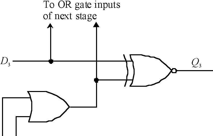
3. The output of an XNOR is HIGH when the inputs agree. If the A B C D inputs all agree with their respective switch settings, then all XOR gates have a HIGH output and the NAND gate output (labeled X) will be LOW; otherwise it will be HIGH.
4. The comparator schematic, drawn with ANSI/IEEE Std 91-1984 symbols, is shown below.
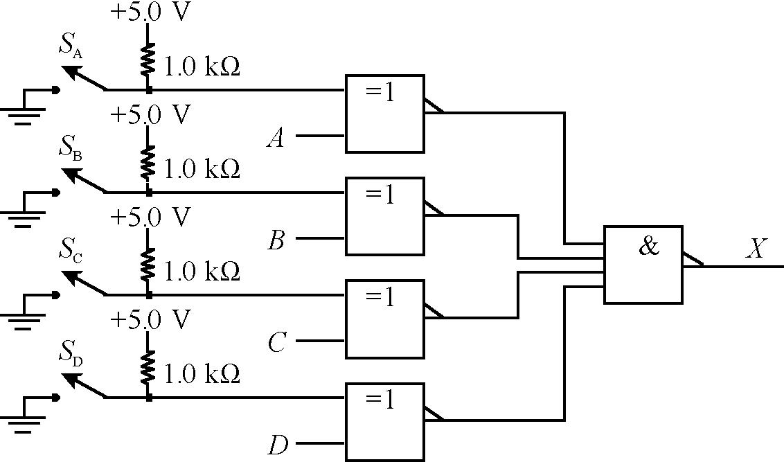
5. XOR function with NAND gates: 6. Four input OR function with 2-input gates:
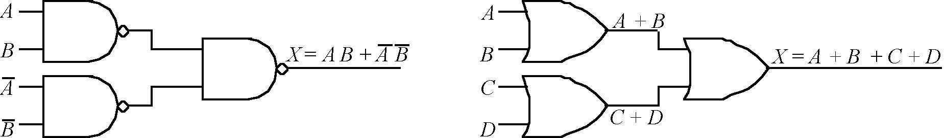
Data and Observations:
TABLE 6-1 TTL 7404
TABLE 6-2 CMOS 4081
VOL(max), low-level output voltage
VOH(min), high-level output voltage
VIL(max), low-level input voltage
IIN(typ), input current ± 10-5 μA
μA* * limited by instruments
Further Investigation Results:
1
Evaluation and Review Questions:
1. A load causes the output LOW to be higher. (The measured LOW with no load was 30 mV; with the minimum load, the measured LOW was 222 mV).
2. R = 2.4 V / 0.4 mA = 6 kΩ
3. VNL(LOW) = 0.3 V VNL(HIGH) = 0.5 V
4. a. Circuit (a) is better. b. The IOH specification is exceeded in circuit (b). In (a), the LED is turned on with IOL and is within the specified limit.
5. Logic levels are specified with reference to ground and can produce incorrect logic if the ground level is wrong. The scope should be dc coupled to assure the troubleshooter knows the ground level of the signal. (Note that in some digital scopes, the ground level is shown with a small arrow to the side of the display.)
6. The transfer curve for an AND gate (with inputs tied together) is shown below. The threshold is expected to occur at +1.6 V.
Plot for Question 6
Data
TABLE 7-2
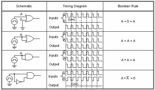
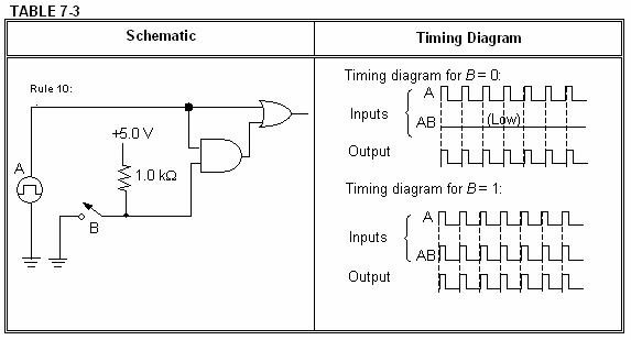
TABLE 7-4
Rule 11: Schematic
Timing Diagram
Timing diagram for = 0: B
Inputs
Output
A + AB = A + B
Timing diagram for = 1: B (LOW) (HIGH)
Inputs
Output
Further Investigation Results:
TABLE 7-5
Truth table for Figure 7-5
TABLE 7-6
Truth table for Figure 7-6
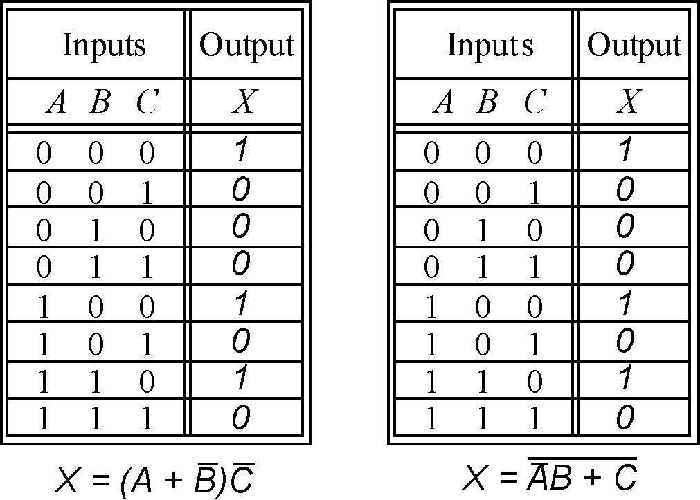
Evaluation and Review Questions:
1. A(A + B) + C = AA + AB + C (distribution) = A + AB + C (rule 7) = A + C (rule 10)
2. A C X
4. Because the two circuits have identical truth tables, they perform the same logic.
5.
6. Answers vary but should follow a logical sequence. An example is:
1. Verify that each IC has power and ground connected and that it is the correct voltage.
2. Select an input that should turn on the LED (such as all switches closed to ground.) With this input, verify that the A, B, and C inputs to their respective gates are all LOW.
3. With all inputs LOW, verify that the output the 4069 gates are both HIGH and that the output of the 4071 is HIGH. Verify that the output of the 4081 is HIGH.
4. Check that the LED is inserted in the correct direction and that there is a path from the output of the 4081 through a 1.0 kΩ resistor through the LED to ground.
Data and Observations
Note: Truth tables 8-2 and 8-3 are identical. Only Table 8-2 is shown.
TABLE 8-2
Truth table for BCD invalid code detector
0 0 0 0
0 0 0 1
0 0 1 0
FIGURE 8-3 Karnaugh Map of truth table for the BCD invalid code detector
Minimum sum-of-products read from map:
Factoring from both product terms gives:
Step 5: Circuit for BCD invalid code detector (replacing OR gate with equivalent NAND gates):
Note that the A switch is not used in the invalid code detector.
TABLE 8-4
Problem Number Problem Effect
1 The pull-up resistor for the D switch is open.
2 The ground to the NAND gate in Figure 8-4 is open.
3 A 3.3 kΩ resistor was accidentally used in place of the 330 Ω resistor.
The D input will be an invalid HIGH when the D switch is open. The circuit will perform normally except is susceptible to noise.
The LED will not turn on under any conditions since there is no return path for LED current
Circuit operates normally but LED is slightly dimmer (may depend on the LED).
4 The LED was inserted backward. The LED will not turn on under any conditions.
5 Switch A is shorted to ground. The A input is not used so it will have no effect.
Further Investigation Results:
TABLE 8-5
Truth table for BCD numbers divisible by three
0
FIGURE 8-5 Karnaugh Map of truth table for BCD numbers divisible by three.
Minimum sum-of-products read from map:
:
1. The path from the OR gate to the NAND gate may be open or the inputs to the NAND gate may both be shorted to D. To troubleshoot the problem, put the circuit in state 1000 or 1001 and test the logic at the OR gate output and at the input of the NAND gate.
2. Equivalent circuit for Figure 8-4 using only NOR gates:
3. The A input was not connected in the circuit in Figure 8-4 because the A variable was eliminated by Boolean algebra from the output expression.
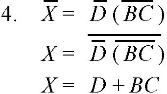
5. Sum of products (SOP) form X = BD + CD. Product of sums (POS form) X = D(B+C). This can be done by factoring or by reading the 0's directly from the map (see Appendix B of text).
6. Implementation from the expression in step 2 (X = BD + CD) is shown in the schematic below:
The model-2 of the perfect pencil machine is a combinational logic circuit that delivers a pencil or change for certain combinations of inputs representing coin switches. Coin switches are provided for one nickel, (N1), two dimes (D1 and D2), and a quarter (Q). (Only one nickel switch is used to simplify the problem). The two dime switches are stacked on top of each other such that D1 is always activated before D2. The truth table has a number of don't care (X) entries, considered to be impossible inputs as described in the experiment. For example, D2 cannot be inserted in the machine until D1 has activated its switch and more than two coins cannot be entered in the machine. These "don't cares" allow the logic to be simplified considerably.
TABLE 9-2
Truth table for model-2 perfect pencil machine
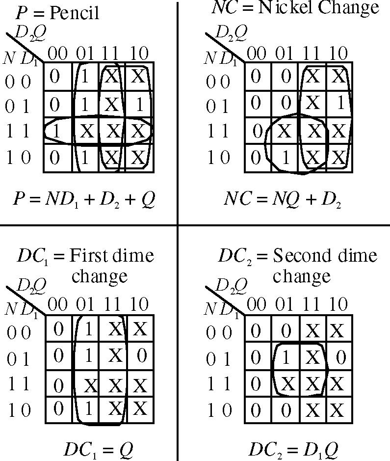
A simplified implementation is shown (switches not shown). The output logic from the maps has been inverted to light LEDs with a LOW rather than a HIGH in keeping with TTL specified IO values.
Further Investigation Results:
This investigation requires the student to modify his or her experiment to use only 2-input NAND gates. The two circuits for dime change logic already meet that requirement. Modifications for the pencil and nickel change logic are shown below:
The model-2 Molasses Tank controller uses standard combinational logic but one of the inputs to the truth table is the output valve logic, VOUT, to produce latching action using feedback. The truth table for the output valve is given in the experiment and the truth table for the alarm, A, and the input valve, VIN, are given here. (The input valve is implemented in the Further Investigation with an extra Karnaugh map provided in the manual for this). Maps for these three outputs are also shown. (The heater output was not required in the experiment, but could be implemented as H = TC LL.) A circuit implementation using inverters and NAND gates is shown (note that A is implemented after applying DeMorgan’s theorem). Active LOW outputs are used for the LEDs as given in the truth tables. Other implementations are possible.
Multisim files for the Model-1 controller are available on the website that was described previously. The file Exp-10nf illustrates how the feedback avoids the oscillation that could occur if the high level detector was the only control for the outlet valve by not closing the valve until the lower level is sensed.
InputsOutputs
Data and Observations
The connections to the adder needed to complete the circuit in Figure 11-2 for a binary to excess-three conversion circuit are:
input: connect to:
B4 A>B
B3 Ground
B2

B1 +5.0 V
C0 Ground
Results for the binary to excess-3 conversion are given in Table 11-4. The inverters are considered part of the display, therefore, logic shown on Table 11-4 is before the 7404 inverters (a logic 1 turns ON an LED).
TABLE 11-4
Further Investigation Results:
TABLE 11-5
Truth table for Figure 11-2 Truth table for overflow error.
Inputs
D C B AA D C B A ' Outputs
0 0 0 0
0 0 0 1
0 0 1 0
0 0 1 1
0 1 0 0
0 1 0 1
0 1 1 0
0 1 1 1
1 0 0 0
1 0 0 1
1 0 1 0 1 0 1 1
(Binary)(Excess-3) 0 0 0 1 1 0 0 1 0 0 0 0 1 0 1 0 0 1 1 0 0 0 1 1 1 0 1 0 0 0 0 1 0 0 1 0 1 0 1 0 0 1 0 1 1 0 1 1 0 0 1 0 0 1 1 1 0
1 1 0 0 1 1 0 1 1 1 1 0 1 1 1 1
Evaluation and Review Questions:
FIGURE 11-5 Karnaugh map for overflow error.
X = AB + AB 444444 ΣΣ X = AB + AB 444444 ΣΣ +5.0
1. a. The input to the 7404 will see an illegal logic HIGH, causing the A' LED to be on. b. Approx 1.6 V.
2. The carry-out (C4) of the lower order adder is connected to the carry-in (C0) of the higher order adder. The schematic is shown in text as Figure 6-12(a).
3. It is the carry-in.
4. Connect the B inputs of the upper 7485 to 1000 and the lower comparator B inputs to 1100. Connect cascading inputs on both so that A=B inputs are HIGH; all other cascading inputs are LOW.
5. To form the two's complement, invert the bits of the subtrahend and add one by connecting the carry-in to a HIGH.
6. An additional voting switch can be connected to the carry-in logic of the parallel adders.
Data and Observations
TABLE 12-1
Truth table for 2-bit comparator A≥B.
Inputs A A B B 2121 Output
0 0 0 0
0 0 0 1
0 0 1 0
0 0 1 1
0 1 0 0
0 1 0 1
0 1 1 0
0 1 1 1
1 0 0 0
1 0 0 1
1 0 1 0
Figure 12-4
Further Investigation Results:
TABLE 12-2
Truth table for even parity generator.
Connect
0 0 0 0
0 0 0 1
0 0 1 0
0 0 1 1
0 1 0 0 0 1 0 1 0 1 1 0 0 1 1 1
1 0 0 0 1 0 0 1 1 0 1 0 1 0 1 1 1 1 0 0 1 1 0 1 1 1 1 0 1 1 1 1
Figure 12-5
Evaluation and Review Questions:
1. The BCD invalid code detector can be designed as shown:
3. The input which affects the second half of the truth table is the A2 input. Place the circuit in a fault condition and check the inputs to the multiplexer beginning with the A2 input.
4. The inverter output is used with minterms 0, 1, 10, and 11. However it will be incorrect only when B1 should be HIGH - which is a fault condition for minterm 0 and 10. Place the circuit in one of these fault conditions and check the appropriate inputs to the multiplexer. Since the multiplexer input is incorrect, the troubleshooter is led to test the inverter and discover the fault.
5. The lines on the truth table that would be incorrect are A
All other lines will read correctly.
6. Odd parity can be obtained from the Y output of the 74151A.
Traffic Light Output logic (Figure 13-6):
Connect 1Y1 to Main Yellow and to Side Red through the 7408 AND gate. Connect 1Y3 to Main Red through a 7408 AND gate and to Side Green. Connect 1Y2 to Main Red through a 7408 AND gate and to Side Yellow. The enable (G1) is wired LOW with switches to the A1 and B1 select inputs. The circuit is shown below:
Figure 13-8
Timing diagram for step 5
Further Investigation Results:
The NAND gate serves as a decoder for a particular output state from the counter. The decoded output then enables the decoder and lights a corresponding LED. As long as the CLK input to the counter is above approximately 100 Hz, the LED appears to be on steady. Different LEDs can be selected by changing the decoder's inputs.
:
1. Use one-half of the 74LS139A for the least significant four bits and the other half for the most significant four bits. Use the enable input on each decoder for the third select input, inverting it for the most significant four bits.
2. To emphasize the active-LOW inputs and outputs.
3. Gray code is useful to prevent glitches in the decoded outputs.
4. a. The input is an illegal HIGH, preventing the 1Y0 and the 1Y1 outputs from being selected. b. The input is LOW, preventing the 1Y2 and the 1Y3 outputs from being selected.
c. The chip is not selected; therefore all outputs will be HIGH.
5. The sequence of the lights would be incorrect. This can be corrected by reversing the output logic for states 2 and 3. The disadvantage is possible glitches in the decoded outputs.
6. The LED will be on whenever C is open (HIGH) or if C and B are closed (LOW) and A is open (HIGH). (Multisim file is used for illustration.)
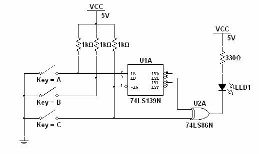
Step 3 Observations: The output of the latch changes only when the switch makes initial contact with the A or B terminals. The latch does not change when the switch is "bounced".
Step 5 Observations: As long as the enable is HIGH, the output (Q) follows the pulse generator input. When enable is LOW, changes on the D input are not seen on the output, however; the outputs can be latched by grounding either one momentarily, even when enable is not asserted.
Step 6 Observations: The burglar alarm basically illustrates the functions of the D latch. When enable is asserted HIGH, the opening of a door or window switch causes the alarm LED to latch on. Closing the door or window switch has no effect on the output. The alarm LED is turned off by closing all switches (or placing it in standby) and pressing the reset pushbutton.
Step 7 and 8 Observations: The setup time specification for a 7474 is 20 ns. The four inverters provide sufficient setup time to read the pulse as a HIGH, causing the output to remain a constant HIGH. When the delay is removed, the output is a constant LOW.
Step 10 Observations: The D flip-flop needs setup time as shown with the clock delay circuit. When sufficient setup time is given, the output will go HIGH; otherwise, it is LOW. The preset and clear inputs are asserted with a LOW input and are observed to be asynchronous inputs. With the clock delay in place and connecting the Q to D, the scope signal can be made to appear as if timing is changing when in fact it is not. (Trigger from the clock to show the timing problem).
Further Investigation Results:
The serial parity test circuit changes the parity every time a logic 1 is received but does not change parity when a logic 0 is received. The circuit has an advantage over the parallel parity test circuit in Floyd's text only when the data is already in serial form and needs to be tested. In this case, the serial tester circuit is simpler and just as fast.
Evaluation and Review Questions:
1. The switch debounce circuit requires two contacts (throws) because the output will not change if a single contact were used.
2. No. With NOR gates, the output would change as the switch pole is first moved from the contact but the other NOR gate output would be unaffected – causing bouncing to be seen on the output. A similar problem would occur on the other contact.
N.C. Switches (doors, windows)
N.C. Switches (doors, windows) Reset Reset
5. There are a several possibilities. Among them are:
1. Reset or enable switch stuck LOW.
2. Open path to the alarm LED including open resistor or open diode.
3. Faulty NAND gate (open output on lower right NAND gate, shorted output on top right gate, etc.) The most likely fault is an open connection rather than a faulty component.
6. A latch would oscillate very rapidly whenever the data was HIGH.
The fallen carton detector is a sequential logic circuit which is designed to detect if a carton, moving on a conveyor belt, is upright or has fallen over. If the carton has fallen, the circuit is to trip a solenoid (indicated by an LED). The circuit can be implemented with a D flip-flop as shown. Student circuits may vary.
(see discussion)
Students will need to experiment to determine optimum series resistors (shown as R1 and R2) to use with the photocells and with the particular room lighting. With a CdS photocell, a value of about 10 kΩ will work in normal room light when connected to a 7474 D flip-flop. The voltage will be LOW when uncovered (< 0.2 V) and will be HIGH (> 3.0 V) when covered.
Further Investigation Results:
As the carton is sent into the reject hopper, a photocell can sense its presence. The photocell output can be connected to the CLR input of the D flip-flop to produce a LOW input when it is covered by reversing the photocell and the series resistor. Because TTL logic requires more current to pull it down, the value of R3 must be much smaller than in the first circuit. A value of 150 Ω worked well with the photocell and the particular room light tested. A reset button is also connected to the CLR input of the D flip-flop. The modified circuit is shown below.
Data and Observations
Step 1 Observations: The preset and clear inputs are asserted with a LOW input and are asynchronous. When both are LOW at the same time, both Q and Q are HIGH.
Step 2 Observations: The truth table is verified – Q follows J when the J and K inputs are different. The output does not change when both inputs are LOW and the output toggles when the inputs are both HIGH. The output is observed to change on the trailing edge of the clock. The output duty cycle is seen to be 50%.
Step 3 Observations: The circuit toggles for each clock pulse.
Step 4 Observations: The ripple counter divides the input frequency in two for each stage as shown in the timing diagram. QA is ½ the Clock frequency; QB is ¼ the clock frequency.
Further Investigation Results:
The 7476 measured and specified values are:
Measured tPLH = 20 ns. Manufacturer's specified tPLH = 16 ns (typ), 25 ns (max).
Measured tPHL = 25 ns. Manufacturer's specified tPLH = 25 ns (typ), 40 ns (max).
The 74LS76A is faster with specified values as follows:
Manufacturer's specified tPLH = 15 ns (typ), 20 ns (max). (Data is from ON Semiconductor.)
Manufacturer's specified tPLH = 15 ns (typ), 20 ns (max). (Data is from ON Semiconductor.)
Evaluation and Review Questions:
1. An asynchronous input is independent of the clock and can affect the output without the presence of a clock signal. A synchronous input can only affect the output when a clock signal is present.
2. a. Assert the preset input ( PRE ) which is asynchronous.
b. Clock the flip-flop when J is HIGH and K is LOW.
3. The output is latched.
4. If Q is connected to J and Q is connected to K, the clock will not change the output logic.
5. The CLK input is open; the Q output is shorted LOW; the CLR input is shorted LOW.
6. Green LED could be open, 390 Ω resistor open, +5.0 V supply not connected to 390 Ω resistor, bad 74LS76A.
TABLE 17-1
Data for 74121 monostable multivibrator Quantity Computed Value Measured Value
Timing Resistor, RT 7.14kΩ 6.89kΩ
External Capacitor, CEXT 0.01 μF 0.01μF Pulse
W
TABLE 17-2
Data for 555 timer as an astable multivibrator Quantity Computed
Resistor, R1 7.5 kΩ 7.46kΩ
Resistor, R2 10 kΩ 10.1kΩ Capacitor, C1 0.01 μF 0.01μF
5.24kHz 5.50kHz
Step 3. Input logic levels and generator connection: To trigger the 74121 with a leading edge clock, either A1 or A2 must be held LOW and the signal generator is connected to the B input.
Step 5. Observations as the frequency is raised to 50 kHz: The pulse width remains the same; it does not stay HIGH when the frequency is increased.
Step 8.
Capacitor waveform Output waveform Plot 1
Step 9. Observations with a short across R2: The output stays HIGH except for a short "spike" that appears each time a new cycle is initiated.
Step 10. Various solutions are possible. One solution is to modify the circuit shown in Figure 17-2 by changing R2 to 3.3 kΩ. (The calculated value is 3.45 kΩ.)
Further Investigation Results:
Both timers need trailing edge triggers that can be obtained on the 74121 by connecting A1 and A2 together and connecting B HIGH (see Figure 17-1, 3 lines from the end of the table). The manufacturer specifies that the external resistor cannot be larger than 40 kΩ. An approximate 4 s pulse can be obtained by selecting a 150 µF capacitor and a 39 kΩ resistor as shown in Figure 17-1 (computed = 4.1 s). A 25 s pulse can be obtained by selecting a 1000 µF capacitor and a 36 kΩ resistor (computed = 25.2 s).
Evaluation and Review Questions:
1. A non-retriggerable monostable multivibrator ignores any triggers that occur during the timing cycle.
2. a. 0.036 µF.
b. Select an external variable resistor. For the computed capacitance, the external resistance needs to vary from 2 kΩ to 10 kΩ
3. Largest recommended resistor is 40 kΩ. The largest capacitor is 1000 µF. With this combination the pulse width is 28 seconds.
4. Duty cycle = 50.1%; frequency = 400 Hz.
5. The required frequency is 0.083 Hz. The sum of R1 + 2R2 = 1.72 MΩ. From the duty cycle equation, the resistors are found to be: R1 = 0.36 MΩ and R2= 0.68 MΩ
6. The voltage ranges from +5.0 V to +10.0 V.
Data and Observations
Waveforms from step 1:
Waveforms from step 2:
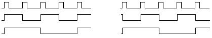
Counter is a down counter.
Waveforms from step 3: (same as step 1)
Clock
Counter is an up counter.
Waveforms from step 4: (same as step 2)
Counter is a down counter.
Waveforms from step 5:
Counter is an up counter.
Waveforms from step 6: reset “spike” Clock B
Counter sequence is 0 - 1 - 2 - reset. The short "spike" is caused by the reset in state 3.
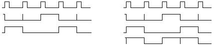
state 0
The decoded output shows a "glitch" when both A and B change together.
Notice that the "glitch" in step 5 is a consequence of detecting state 3 and using it to reset the counter. The "glitch" in the state zero decoded output is different. It is caused by the fact that the counter is momentarily in state zero due to propagation delay between the two flip-flops.
Waveforms from step 7:Waveforms from step 8:
Note glitch
The sequence is 0-1-2-3-4-5-6-7-8-9 - reset (momentarily in state 10)
The XOR gates act as inverters when the Up switch is closed and act as buffers when it is open. By inverting or not inverting the waveforms, the counter can appear as an up or a down counter. The disadvantage of the method is that the reversal of the bits when the switch is open or closed will cause the count to change at the switching time.
1. a. The A signal is 4X faster than the clock. Since the measurement shows that it is 4.00 kHz, the clock frequency is 1.00 kHz.
b. If you want to check the time relationship of any other signal with respect to the displayed signals, it is easier to make the comparison with the slower waveform. Since it is a digital scope, the two channels are digitized together and so this reason is for convenience only. If this were an analog scope, a timing error can be made by triggering on a faster signal to observe (and compare) a slower signal.
2. a. The count sequence is truncated by decoding one number more than the ending number and using the decoded output to reset the counter.
b. The procedure produces a glitch because the counter is in the decoded state for a very short interval.
3. The clear input may be shorted LOW, producing a HIGH output on both flip-flops; the line from Q to D on the A flip flop may be open causing an (invalid) HIGH to be clocked into the A flip-flop at each clock pulse.
4. The time relationship determined from a two channel oscilloscope could be interpreted incorrectly because the scope can be triggered by any arbitrary clock pulse. Relative timing is unambiguous when the various waveforms are compared to the slowest waveform.
5. a. Circuit: b. Waveforms:
6. The sequence is 0-1-2-3-4-5-8-9-reset (momentarily in state 10)
Reset: waveforms repeat
TABLE 19-2
Analysis of synchronous counter shown in Figure 19-3
State diagram:
Note the glitches in the decoded outputs for state 0 and state 3.
Step 4: State diagram:
TABLE 19-3
Analysis of counter shown in Figure 19-4
Plot 1
Step 6: State diagram:
Repeats..testunusedstates:
Returnstoatestedstate(mainseq)
Returnstoatestedstate(mainseq)
Returnstoatestedstate(mainseq)
Further Investigation Results:
The circuit shows the letters for the word C-L-U-E in the seven segment display.
Evaluation and Review Questions:
2. The sequence is that of a down counter:
3. Full decoding means all possible states must be decoded. Because there are three outputs, full decoding can be accomplished with a 3-to-8 decoder such as the 74LS138.
4. Connect the pushbutton so that it clears the A and C counters and presets the B counter using the asynchronous clear and preset inputs.
5. The counter can be locked in state 3 if there are no clock pulses or if the common preset line is shorted LOW.
6. State 9 (DCBA = 1001) should go to state 1 (DCBA = 0001) but isn’t changing. By observation, three of the F/F’s do not change states for this transition (FFA, FFB, and FFC). FFD should change and isn’t changing, so it is the likely culprit.
Further Investigation Results:
Evaluation and Review Questions:
Note: A variation for drawing Karnaugh maps was presented in the lab book in Figure 20-3 and repeated here for reference. The QB and QA variables are not written side-by-side; rather they are written nearly vertically. Some students find it easier to read the map to relate the number to the variable when they are drawn like this.
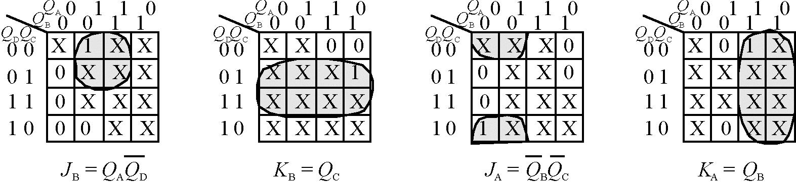
2. Since the largest binary number in the circuit for the experiment is less than ten, a BCD to sevensegment decoder (such as the 74LS47A) can be used to convert the binary number into a value that can be shown in a seven-segment display.
3. The reset button is connected between ground and the preset input of FFC and FFB; it is also connected between ground and the clear input of FFA
4. The count sequence can be reversed by reversing the A and C bits from the counter. This can be accomplished by using a 2-input MUX, such as the 74LS157. (Note that only a part of the 74LS157 is shown.)
5. When the counter goes from state 3 to state 2, the A output is seen to do a 1 to 0 transition. Likewise, when the counter goes from state 6 to state 4, the B output does a 1 to 0 transition. These transitions are unique, therefore trigger by connecting the A and B outputs to the A1 and A2 trigger inputs of the 74121 (B trigger is HIGH). (See the function table for the 74121, given in Figure 17-1).
6. a. The D transition table is shown. The QN+1 output follows D at the clock edge.
b. The J-K flip-flop is more versatile because it has the latch and toggle states. For this reason, there are X’s on the transition table which aid in designing a simpler circuit for irregular count sequences.
Note - Table 21-1 lists present states in the gray-code sequence selected for the controller (0-1-3-2) rather than binary sequence. Table 21-1
Present State Next State
Schematic:
Conditions Input Product Term for Data Selector-1 Input Product Term for Data Selector-0
21-4
Step 6: To return to the first state, the vehicle sensor must be LOW and remain LOW (no vehicle on side street).
Further Investigation Results (TTL)
The first idea is sound; the short timer can be eliminated if states change in no less than 4 s. The equations would need to be changed to implement this. The second idea will not allow the state machine to function as designed.
Evaluation and Review Questions:
1. Gray code is selected to avoid false states due to decoding glitches.
2. The long timer (TL) and the vehicle sensor (VS) must both be HIGH.
3. A third flip-flop is needed for the counter and the MUXs would be changed to 3-to-8 lines.
4. Connect the Y output from the MUXs to J; this line is inverted and connected to K
5. Refer to the 7th line down on the table in Figure 17-1. In order to have both A inputs trigger on a trailing edge, B must be HIGH.
6. The next state will sequence only if the long timer (TL) is LOW and the vehicle sensor (VS) is HIGH. Because the long timer is okay, test VS. If it is okay, check the counter for clock pulses and correct inputs on D. If okay, check asynchronous inputs, power, and grounds.
Schematic for Johnson Counter: Schematic for Ring Counter:
Timing diagram for Johnson counter:
Timing diagram for ring counter loaded with 1110:
pushbuttonsN.O. pushbuttons
The Serial predict data is compared with the data from the device when the Strobe line goes HIGH as shown in the following timing diagram:
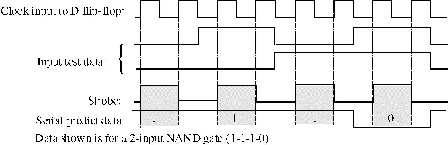


1. The QD output of the first 74195 is connected to the inputs of the second. The output from the second 74195 is connected to the inputs of the first.
2. To prevent the data from shifting more than one position for each clock pulse.
3. a. 101-110-011. b. 101-010-101. (An interesting but generally not useful result!).
4. After the stored data has been clocked out, the same input data will appear at all outputs.
5. The 8 active states are shown in the diagram. (Repeats after 8 states).
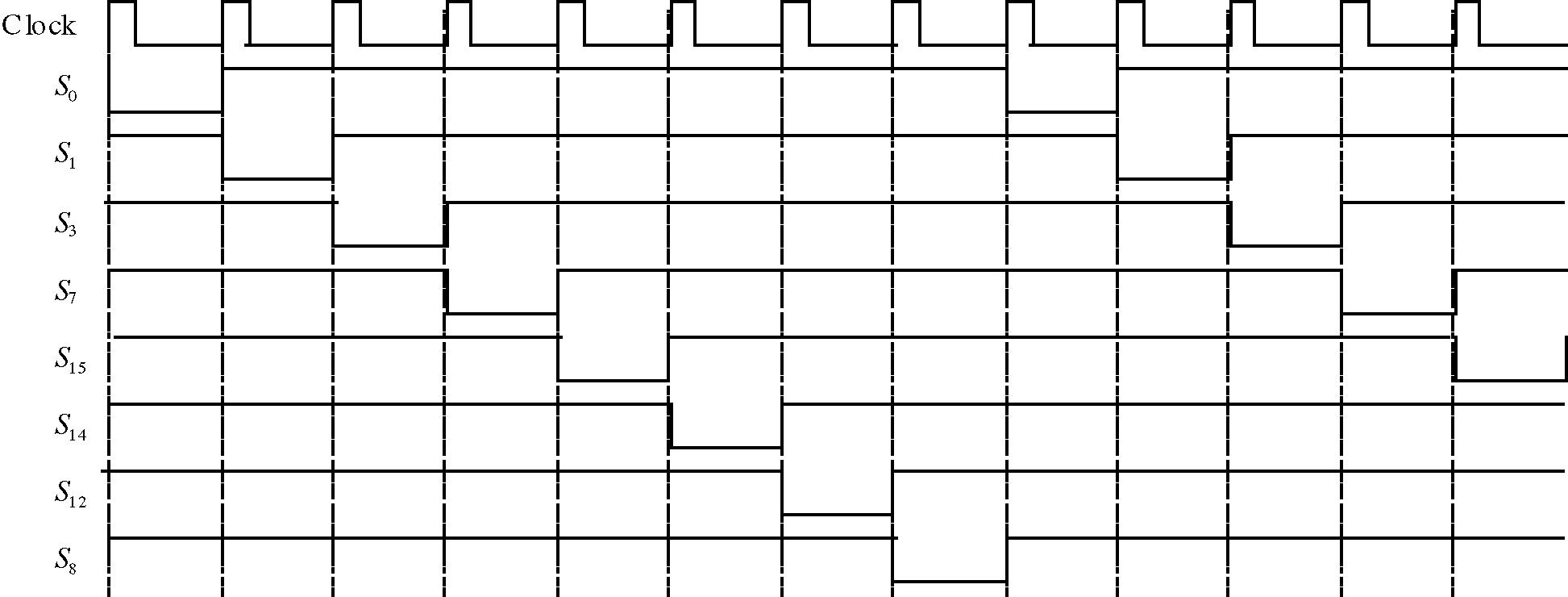
6. Politely tell the boss that a normal ring counter is self-decoding and that a decoder is not necessary.
Data and Observations:
Step 2: After loading the data, the start bit flip-flop is observed to have a LOW (LED on). Data from the shift register can be seen to move to the right at each clock pulse. The data at the QA output moves to the Serial data out position after 5 clock pulses. The register is then filled with HIGHs (LEDs all off) until reloaded.
Step 3: Sample calculations of the resistors for the 555 configured as an astable multivibrator are given. (See Figure 17-2 for the circuit for the astable configuration.) f =
Let C =0.1 μF. Then:
With the values selected above, the duty cycle is 81% and the frequency is 985 Hz.
Step 4: Because of the asynchronous relation between the data clock and the SHIFT/ LOAD pulse, the time between the serial data out and the SHIFT/ LOAD and the start bit is not fixed.
Start bitStop bits
Serial Data Out
SHIFT/ LOAD
Step 5: The circuit to send exactly five clock pulses is shown in the shaded box. When the start bit is detected, the data is shifted in the 74195. The frequency of the pulse generator is set to twice that of the transmitter in order to generate one complete pulse with every two clocks. (The 7493A counts to ten during this process.)
Serial data in
Circuit to generate exactly 5 clock pulses
The receiver pulse generator is set twice as fast as the transmiitter's pulse generator because the circuit that generates 5 clock pulses divides the receiver frequency by two. The generator frequencies should be close to the 2-1 ratio, but it is not necessary to be exact. Five data pulses are used to send the start bit right through the receiver (into the "bit bucket"), moving only the data that was set at the transmitter into the receiver. The stop bits are represented by HIGHs, and since the line is held HIGH (no transition), the receiver will not be clocked until a new start bit is received.
Evaluation and Review Questions:
1. The J-K inputs are connected HIGH. This HIGH is shifted into the 74195A at each clock pulse.
2. The first bit is a start bit which is not part of the data. The extra clock pulse causes it to be clocked through the receiver's shift register.
3. The start bit transition is a falling edge (HIGH to LOW). The NAND gate, which acts as an inverter, changes the active edge so that it can trigger the 7474 with a leading edge.
4. a. The numbers to be added are entered into the input shift registers. The full adder produces the sum and the carry bit sequentially as each bit is shifted through the input registers. As the sum is produced, it is moved sequentially through the output shift register. The carry-out flip-flop stores the carry bit to be added to the next most significant bit.
b. The output shift register will contain 0011; the carry-out flip-flop will contain 1.
5. A 74195A shift register can be configured as a ring counter. The register is loaded with the pattern 1000 which is recirculated. The outputs are taken from either QA and QC or from QB and QD
6. If the start bit flip-flop is loaded with a HIGH instead of a LOW, the start bit will not occur. This could occur if the clear input to the start bit flip-flop were open.
The baseball scoreboard is a sequential logic circuit that can be implemented with shift registers or with a counter. One possible solution, using 74175 quad D flip-flops connected as shift registers is shown. Switch debounce is provided by the 555 timers.
Strikes Pushbutton Balls Pushbutton
Student answers will vary. The inning display can be set up as a 16-position shift register with a single LED on at any given time. Another approach is to use a 16-bit DMUX driven with a manually clocked 4-bit counter controlling the select inputs of the DMUX. Outs can be connected as a 2-bit shift register made from D flipflops controlled by a debounced pushbutton, similar to the circuits shown above.
The schematic for the addition to the security entry system is shown. The combination is entered as the complements of the BCD numbers (95614) stored in locations 0000 through 0100. Location 0101 should have 0000 stored to blank the 7-segment display after the last number.
Further Investigation Results:
The 7493A is set up to count from 0 through 5 by connecting the QB and QC outputs to the reset inputs and QA output to the CLK B input.
Evaluation and Review Questions:
1. For this experiment, address and data switches are set manually, and do not change. Therefore, it is not necessary to debounce the start push-button. It is included in the system because this is a simulation of a portion of a larger system.
2. The number to be stored is 0000. The output is the complement of the stored number.
3. a. Locations are addressed by binary numbers. On chip decoding means that the binary addresses are converted internally to the specific row information needed.
b. Outputs are in a high-Z state.
4. 256 locations
5. a. The word length needs to be expanded to 7 bits by expanding memory.
b. Locations would store the encoded combination for the seven segment display.
6. When R/ W is LOW, the outputs are the complements of the data inputs.
Note: This experiment is a tutorial exercise that introduces the Quartus II design tool from Altera. Students work at a computer that has the latest version of Quartus II software loaded. The software is available at www.altera.com. Click on Download, Quartus II software, and follow the instructions to download the free web edition. A license file is necessary which is specific to that computer. The steps in this tutorial exercise illustrate schematic entry, using the model-1 Molasses Tank outlet valve logic as a basic circuit. It was selected for this exercise because it has a variation on strictly combinational logic (adding feedback) and the software simulation can show this effect nicely. The TTL version of the circuit is shown for reference.
If you want to go beyond this basic introduction to the software, you will need a PLD trainer board, such as the PLDT-2 from RSR Electronics or the Altera board, available from Altera. The trainers allow students to download the experiment to hardware and test the results. For detailed instructions on using both Altera and Xilinx PLD programming software and including downloading to various trainers, see the lab manual Experiments in Digital Fundamentals with PLD Programming by David Buchla and Doug Joksch. Five trainers are discussed in detail in the PLD manual, with diagrams and tables for the boards, pin assignments, and more. The final output signal that the student should draw is shown on the display. The VOUT signal goes LOW when the valve is open. Notice that it opens only after the upper level sensor is covered but closes only after the lower level sensor is uncovered (hence the hysteresis).
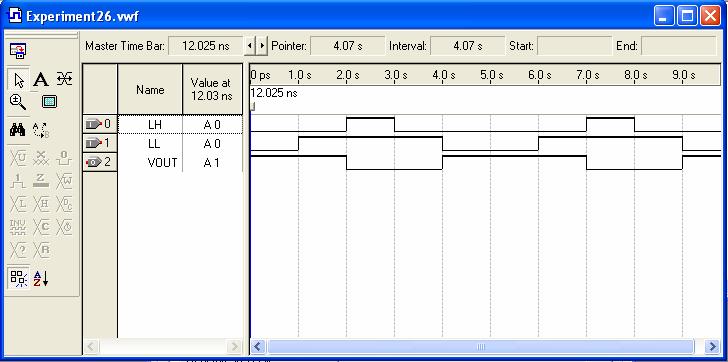
Quantity
Table 27-1 Plot 3Plot 4
Measured Value
Steps 7 and 8: The digital light meter has an oscillating behavior because of the tracking A/D converter as shown. The D/A output waveform increases its dc level from approximately 2 V to approximately 0.2 V as the light level increases.
Further Investigation Results
Pulse Generator:
Analog output: (pin 4 of DAC)
Measured data for the circuit in Figure 27-1 is shown on the table. The voltages listed are at the thresholds.
Evaluation and Review Questions:
1. a. Binary 1010 is represented by 1.30 V. b. The output frequency is 62.5 Hz.
2. ( 1.95 V)/255 steps = 7.65 mV/step
3 a. The output voltage is larger because the reference current is larger. b. The resolution measured in volts/step increases. (Note that if measured simply by number of bits, the resolution is unchanged.)
4. The oscillation is caused by the quantizing error between the analog voltage from the photocell and the digitized representation from the converter. If the least significant bit is not used, the oscillation can be eliminated.
5. a. Decrease the reference current by increasing the 5.1 kΩ resistor or decrease the 2.0 kΩ load resistor.
b. No. The change only effects the digital display, not the basic sensitivity of the photocell.
6. A higher clock frequency causes the meter to respond faster to changes but has the disadvantage of causing the display to change rapidly, making it more difficult to read.
Note: This experiment is an introduction to microprocessor concepts and uses a tutorial format to acquaint students with how computers store data, the Intel register structure, a few assembly language instructions, and an introduction to programming. Debug is the program used for the tutorial and is available on any DOS based computer. Debug is limited to the 16-bit registers. No hardware is needed and questions are answered in the Procedure section. Although some steps do not require a student answer, the sequence of the steps is shown here to aid in following the experiment.
Procedure:
Step 1: Student enters Debug and observes some Debug commands.
Step 2: Answers will vary depending on the computer. The equipment status word 27 C2 given as an example is interpreted as follows:
Number of parallel printer ports attached = __3__
Number of serial ports attached = __1___
Number of diskette devices = __1___
Initial video mode = ___80 x 25_____________
Math coprocessor is present? ___yes______
Diskette drive is present? ___yes______
Step 3: Answers will vary depending on the computer.
Step 4: The right side will be filled with zeros since 30H represents ASCII 0.
Step 5: Location DS:20 is changed to 31H (ASCII 1).
Step 6: The display will show DS:0020 31 30 DS:0050. (DS will have the current data segment value). This indicates that location DS:20 does not correspond to location DS:50. The two corresponding data points in these locations are 31H and 30H.
Step 7: The 16-bit register set is displayed.
Step 8: The command sequence is R BX <cr> followed by :200 <cr> and R CX <cr> followed by :F003 <cr>
Step 9: The Debug assembler is used to enter a short code.
Step 10: The code in step 9 is traced. The caps lock is activated (and shown with an LED).
Step 11: Each loop toggles the caps lock function; the light will turn on and off twice before exiting the loop.
Step 12: “Byte-size” data is entered into 17 locations (the 17th location is DS:60 and will have a zero entered as an end of record signal.
Step 13: The modified “BIG” code is assembled. After it is executed with the “go” command, AX will have the largest number in the list, BX will contain 0060H (the last location), and CX will contain 0000H (the final value of the loop counter).
Step 14: The largest number is observed to have been copied into location DS:60.
Further Investigation Results:
The smallest byte value in the list (from DS:50 to DS:5F will be moved into the AL register and into location DS:60. The AX register will show FFH. BX contains 0060H (as before) and CX contains 0000H (as before).
Evaluation and Review Questions:
1 The data in step 2 is from the BIOS RAM area, the data from step 3 is in ROM.
2. Locations from DS:1F0 to DS:1FF are filled with the value FAH.
3. D 0:0 9
4. The BIOS work area starts at location 40:0. An example of data that is in this area is information about the peripherals connected to the computer.
5. When any number is XORed with itself, the result is always zero because 0 XOR 0 = 0 and 1 XOR 1 = 0.
6. The LOOP instruction decrements the CX register and jumps to the start of the loop if CX is not zero; otherwise it executes the next instruction.
Step 3: With all switches on the 14532B open, the chip outputs are all LOW, including the GS output as shown on the second line of the 14532B truth table. The transistors act as inverters, causing the corresponding inputs on the 14051B to be HIGH. If the inhibit line is tied LOW on the 14051B, the internal FET switch is closed that connects X7 to the common out/in line. This completes the path from the 555 timer to the LED representing the least significant bit, causing it to blink.
Decoder schematic: The decoder schematic depends on the particular address assigned to each student. As an example, a 7400 NAND gate, shown decoding address 01, is drawn below:
Further Investigation Results:
Answers may vary. A 4-bit counter such as the 7493A may be selected or the student may design a two-bit counter with J-K or D flip-flops (such as the ripple counter drawn in Figure 18-2). The counter output is connected to a 7447A BCD to seven segment decoder similar to Figure 3-2.
Evaluation and Review Questions:
1 a. The transistors are used to provide an open-collector connection to the data bus.
b. The display is an input device. The bus can have multiple input devices connected to it without bus contention problems.
2. Each priority encoder is located at a unique address as determined by the individual decoders.
3. The 14051B can be connected as a MUX by connecting inputs to the X lines and taking the output from the common out/in line. The select inputs behave the same for both configurations.
4. R16 is a current limiting resistor for the LEDs. If it opens, no LED will be on.
5. a. The constant HIGH is connected to the selected output, causing the selected LED to stay on.
b. All LEDs will be off.
6. a. The line will be LOW.
b. A data line can be pulled LOW by any transistor connected to the line that is conducting because it provides a direct path to ground.
c. Check the address bus to determine which indicator is being addressed.