
Signal & Image Processing : An International Journal (SIPIJ) Vol.2, No.3, September 2011
A SMART CAMERA PROCESSING PIPELINE FOR IMAGE APPLICATIONS UTILIZING MARCHING PIXELS
Michael Schmidt1, Marc Reichenbach1, Andreas Loos2, Dietmar Fey1
1Chair of Computer Architecture, Department Computer Science, Friedrich-Alexander University, Erlangen-Nuremberg, Germany {michael.schmidt, marc.reichenbach, dietmar.fey}@informatik.unierlangen.de
2TES Electronic Solutions GmbH, Munich, Germany andreas.loos@tesbv.com
ABSTRACT
Image processing in machine vision is a challenging task because often real-time requirements have to be met in these systems. To accelerate the processing tasks in machine vision and to reduce data transfer latencies, new architectures for embedded systems in intelligent cameras are required. Furthermore, innovative processing approaches are necessary to realize these architectures efficiently. Marching Pixels are such a processing scheme, based on Organic Computing principles, and can be applied for example to determine object centroids in binary or gray-scale images. In this paper, we present a processing pipeline for smart camera systems utilizing such Marching Pixel algorithms. It consists of a buffering template for image pre-processing tasks in a FPGA to enhance captured images and an ASIC for the efficient realization of Marching Pixel approaches. The ASIC achieves a speedup of eight for the realization of Marching Pixel algorithms, compared to a common medium performance DSP platform.
KEYWORDS
1. INTRODUCTION
Marching Pixels (MPs) are an alternative design paradigm, e.g. to analyze global image attributes like the zeroth and first moments of objects with an arbitrary form and dimension. Subsequently, the centroid of these objects can be determined. This method is biologically inspired, e.g. by an ant colony, where each artificial ant has a strongly limited complexity but the local interaction of all individuals together results in a more complex system behavior. Using the biological inspired MPs in a two-dimensional SIMD-structure an artificial computer architecture provides emergent and self-organizing behavior. The resulting ASIC presented here can be a part of an embedded stand alone machine vision system.
A problem which basically occurs is that the input images from an image sensor, which should be processed by the MP architecture, are often noisy or need to be converted or enhanced. Commonly, some image pre-processing operations are required [1], before the input image can be processed efficiently by the ASIC. Image pre-processing operations are data and computationally intensive task. Commonly, they are realized with Sliding Window Operations (SWOs), a form of
DOI : 10.5121/sipij.2011.2312
Marching Pixels, Full Buffering, Machine Vision, Sliding Window Operation, FPGA137
Signal & Image Processing : An International Journal (SIPIJ) Vol.2, No.3, September 2011
2D stencil codes [2]. Stencil codes operate on regular matrices. They update the values using neighboring array elements in a fixed pattern. This pattern is called the stencil. For the processing of a pixel with a SWO, a certain number of neighboring pixels and optionally a number of coefficients are required, e.g. for convolution operations. Examples for such SWO based image pre-processing operations are morphological operations like Erosion, Dilatation, Open, Close and Thinning for binary images and digital filters like Median filter or feature detectors like the Sobel Edge Detector for grayscale images. There exist a lot of more image pre-processing operations based on SWOs. FPGAs are well suited for the implementation of such SWOs. They are very flexible and allow a parallel processing on both, a fine-grained and a coarse-grained level. Hence, the image pre-processing operations can be implemented efficiently relating to the application of the machine vision system.
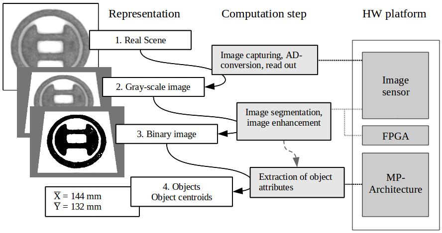
Figure 1 - Data Processing Flow
We will present an image processing pipeline for Marching Pixel approaches which consists of an FPGA with a special buffering architecture for the realization of image pre-processing operations and an ASIC for the efficient processing of MP algorithms. MP algorithms require a lot of resources and, hence, are difficult to implement in FPGAs, especially in low-power FPGAs. Therefore, we favor the realization of an optimized ASIC for the MP approaches and the implementation of required image pre-processing operations should be realized in a low-power FPGA to allow a flexible adaption to the underlying application of the vision system. Figure 1 shows an overview of the image data flow in our proposed architecture. First, an image is captured by an image sensor and converted to digital values. Commonly, gray-scale images are sufficient for a lot of applications in machine vision and some of them require only a binary representation of a scene. Therefore, different processing steps are possible. The gray-scale image can pre-processed by the FPGA and transferred directly to the MP architecture (gray dashed arrow). It is also possible that the image is binarized in the FPGA before or after the image preprocessing and the binarized image is transferred to the MP architecture. The object centroids can then be calculated with the pre-processed binary or gray-scale image. The data is reduced to the center points of the objects and further systems, for example robots, can be controlled with the output.
In this paper we propose two architectures. The first architecture is a special buffering template for FPGAs, for the realization of image pre-processing operations on gray-scale or binary images. The other one is an ASIC for Marching Pixel approaches, to calculate the centroid points of objects for example. The ASIC architecture we have already introduced in [3]. The focus in this Paper is the interaction with an image sensor and an FPGA as image pre-processing unit to build
138
Signal & Image Processing : An International Journal (SIPIJ) Vol.2, No.3, September 2011
up an image processing pipeline for a stand-alone machine vision system.
To realize image pre-processing operations based on SWOs efficiently, it is necessary to implement sufficient buffering strategies within the FPGA, for the data to be processed. The most common buffering concepts are the Full Buffering (FB) and the Partial Buffering (PB) strategy [4], [5]. We favor the FB scheme since it allows a streaming of the data from the sensor to the Marching Pixel architecture, without a buffering of the complete image. This is not possible with a PB strategy, because a pixel has to be loaded several times during the processing. Therefore, the image or at least a part of the image has to be stored in an external memory, before the processed data can be transferred to the Marching Pixel architecture.
We have adapted the standard FB approach to realize a parallel processing of SWOs, if more than one pixel is available from the image sensor per system clock cycle. An example for the processing of two sliding windows with the help of the FB scheme was presented in [3]. We concretized this idea and developed an adapted FB scheme for a parallel processing with an arbitrary degree of parallelization, depending on the available pixels per system clock cycle from the image sensor. The new approach, realized by us, is the pipelining of several of our adapted FB instances, to allow the consecutively processing of several SWOs before the image data is transferred to the Marching Pixel architecture. Hence, several image pre-processing operations can be performed simultaneously while streaming the data from the image sensor to the Marching Pixel architecture. Thus, the overall processing time for the image pre-processing operations and also the latency between image capturing and processing in the Marching Pixel architecture can be reduced significantly.
The ASIC for Marching Pixel algorithms is realized as SIMD architecture. We present a short mathematical derivation of the system and address a hierarchical three-step design strategy to generate a full ASIC layout. For prototyping purposes only a SIMD architecture with a small resolution of 64x64 pixels was designed. The focus in this paper is the realization of object centroid determination with Marching Pixels. The latencies of this determination are compared with those of a software solution running on a common medium performance DSP platform.
This paper is divided into six sections. In the next section we present former work and projects which are related to our architectures. Afterwards, in section three, the mathematical basis for our image processing tasks, especially for the Marching Pixel algorithms, will be explained. In section four our generic image pre-processing architecture will be presented together with some simulation and synthesis results. Afterwards, in section five, our Marching Pixel chip architecture for the determination of object centroids will be discussed. At last, we want to conclude the most important points of our paper.
2. RELATED WORK
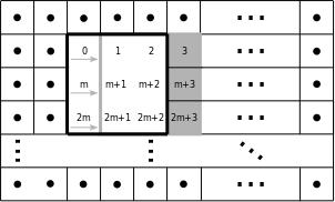
In the following, we assume images with a resolution of m × n pixels, where n is the height and m is the width of the image. Each pixel stores d bits of information, which is d = 1 for binary and d = 8 for gray-scale images. We assume that for the image pre-processing operations, the image is processed with a sliding window from the upper left to the lower right corner. We also assume a Moore neighborhood, which means a stencil size of 3 × 3 pixels, where the center pixel is processed by the SWO.
139
Signal & Image Processing : An International Journal (SIPIJ) Vol.2, No.3, September 2011
Figure 2 - Partial Buffering
Figure 3 - Full Buffering
The PB scheme is illustrated in Figure 2. In the PB scheme, only pixels required for the SWO at the current position are buffered in the FPGA internally, enclosed with bold black lines. For the processing of the next window, three pixels have to be read in which are highlighted with a gray background in Figure 2. Because the image sensor transfers the image pixels consecutively, the image has to be buffered in an external memory. Therefore, a streaming and processing of the data is not possible with this buffering scheme. The advantage of PB is that only a small amount of pixels has to be buffered internally. The FB scheme is shown in Figure 3. The pixels enclosed by the bold black lines are buffered in the internal memory of the FPGA. Two complete image rows and some additional pixels, depending on the stencil, have to be stored internally. In our case, for 3x3 SWOs, this is (2·m+3) pixels. Hence, the FB scheme requires more resources than PB. After the processing of the actual pixel value, the sliding window is moved to the next position which is indicated by gray arrows and the window with bold gray lines in Figure 3. For the processing of the next window, only one pixel has to be read in which is highlighted with a gray background. Therefore, the pixels from an image sensor can be fetched directly by an FB architecture in the FPGA and streamed to the Marching Pixel architecture after processing.
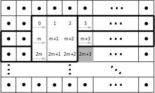
There are a lot of applications where the PB scheme is favored because of the lower resource consumption. Several architectures for shifting a window over an image in 2D shift-variant convolvers are presented in [6]. A PB scheme combined with parallel memory access is used in [7]. Therefore, several external memory modules together with a memory management unit are used. In [8] an efficient multi window PB scheme is proposed for 2D convolution. The goal was to optimize the memory access compared to a standard PB implementation. There are also some approaches which use different buffering schemes for a parallel processing to increase the throughput rate. Yu and Leeser [9] presented an automated tool which allows the adjustment of the parallelism and buffering strategy depending on the application, the on-chip memory and the external memory bandwidth. They propose a so called block buffering, which is based on a PB scheme. A block of pixels is loaded which is greater than the sliding window. Hence, more windows could be processed in parallel and redundant memory accesses can be eliminated. In [10] a parallel processing scheme based on a 2D systolic architecture is presented which can also be classified as a PB scheme. Several windows are processed in parallel and pixels read from external memory are reused efficiently. However, all of these approaches, based on PB, require a storage of the image data in an external memory. A streaming and processing of the data from the image sensor is not possible, because not all redundant memory accesses are eliminated in this buffering scheme. Therefore, we favor the FB approach. It reduces the latency for the image preprocessing operations, because the data can be streamed efficiently during the processing of the SWOs from the image sensor to the Marching Pixel architecture. Considering the capacities of state of the art FPGAs, the increased resource consumption of the FB scheme appears to be acceptable. Furthermore, we favor the FB scheme, because it allows an efficient pipelining of FB instances in order to process several SWOs simultaneously. This is not possible with the PB approach.
140
Signal & Image Processing : An International Journal (SIPIJ) Vol.2, No.3, September 2011
Hard-to-solve classes of image operators are those to determine global image information. An example is the computation of centroids and orientations of large sized image objects with an arbitrary form factor (convex as well as concave). In order to introduce the problems to extract these object attributes, some related work for the Marching Pixel architecture is given in the following. Integrated image processing circuits to obtain zeroth, first and second moments of image objects are presented for the first time in the early 90's of the 20th century. An earlier photosensitive analog circuit with these capabilities is already presented in [11]. The single photo currents generating by the photo diodes are summed up by a two-dimensional resistor network. The centroid and the orientation can be determined by measuring the voltages (which correspond to the moments) at the network boundaries. A further method introduced in [12] describes, how moments of zeroth to second order of numerous small objects (particles) can be determined in a massively parallel fashion within an FPGA. The computation bases on image projections, while a binary tree of full-adders performs a fast accumulation of the moments. A fully-embedded, heterogeneous approach is addressed by [13]. The architecture presented in that paper is based on a reduced behavioral description of a Xilinx PicoBlaze processor. Only the required operators to compute binary images are realized. At all 34x26 processing elements have been connected to an SIMD-processor to compute a tenth of the pixel resolution of an QVGA-image (320x240). The calculation of the bounding boxes of the image objects as well as the zeroth, first and second moments of each of these partitions is performed in parallel. The object centroids and orientations are calculated by a Xilinx MicroBlaze processor. Subsequently, a Xilinx Spartan3-1000 FPGA implementation could be realized to apply the architecture at binary images with VGA-resolution (640x480). Another approach to extract global image information are CNNs (Cellular Neuronal Networks). In [14] a CNN network calculates symmetry axis and centroids of exclusively axial symmetric objects. To apply this method, an object has to be extracted by a preprocessor from a given image. Afterwards, the coordinates of each object pixel has to be transformed into its polar form.
In [15] it was shown by Dudek and Geese, that it is possible to rotate and mirror images in a fast way due to the swapping of neighbored pixels and the use of only local communication mechanisms by Marching Pixels. The present paper affects the analysis of distributed algorithms to extract global image attributes by a two-dimensional field of calculation units (CUs). Each CU has a Von Neumann connectivity to its immediate neighbors. The main difference to the CNNs is the capability of these CUs to store states and to change them in dependence of the states of the CUs in the local neighborhood. The interactions between the CUs cause a information flow beyond the local neighborhoods, which has lead to the concept of Marching Pixels (MP) [16].
In [17] and [18] the finding of object centroids is carried out due the evolving of a horizontal line, where MPs begin to run from the upper and lower edge of each object. During passing through the object vertically the MPs increments the column sums within the object. When opposing MPs meet each other, the upper column sum is added to its lower counterpart and a so called reduction line emerges. The two points of the reduction line, adjacent to the object edge, are defined as left side and right side. Then the evaluation process is described as follows:
At the left side one MP starts and adds up the left sums located on the reduction line.
When the MP reaches the right side on the opposite object edge it returns and adds up the right sums in the same way.
During the MP returns it calculates the difference between the actual right with the stored left sum. When an underflow is detected the object center is found.
This algorithm is useful in the case of convex objects with a adequate form factor. Otherwise, it is possible that the algorithm does not converge in the object centroid. Some theoretical work to the present paper had been done by [19] and [20], especially for the Flooding and the Opposite Flooding algorithm which converge correctly in all cases in contrast to the method mentioned before. Key parts to implement these algorithms in FPGA hardware are presented in [21], but it is difficult to implement more complex MP algorithms, e.g. gray-scale based approaches, for
141
Signal & Image Processing : An International Journal (SIPIJ) Vol.2, No.3, September 2011
sufficient image resolutions in low-power FPGAs. Therefore, we propose the realization of these algorithms in an optimized ASIC architecture and to combine this ASIC with a low-power FPGA for the flexible realization of image pre-processing operations.
3. MATHEMATICAL BASIS
3.1 Image Segmentation
To understand the image processing algorithms for the Marching Pixel architecture, it is important to define a mathematical basis. Let I be an image with a resolution of
pixels (Pi,j) in the following way:
whereas a pixel is defined as: Pi,j = (i , j, xi,j), where xi,j is the gray value for that pixel. To assign a pixel it's gray value
at the coordinates (i,j), we define the function: υ(Pi,j) = xi,j.
The segmentation of gray-scale images can be carried out in different ways depending on the image processing application. The easiest way to create a binary image from a given gray-scale image is to compare the actual gray value υ(Pi,j) of each pixel with an adjustable threshold S:
(1)
else
To get feasible results while executing MP algorithms on gray-scaled images, the following method is recommended:
(2)
All pixels below the threshold are assigned with 0 (image background) whereas all object pixels keep their gray value.
3.2 Bounding Box Computation
The Flooding algorithm is characterized by the generation of a bounding box for each image object. The pixels of the Von Neumann neighborhood of a pixel Pi,j are denoted as { Pi,j-1 , Pi-1,j , Pi+1,j , Pi,j+1 }. In the case of a binary image, all pixels { }1,0
P have the
142
m x n
= ++ + + ninmn mj mj mj ij ijij ij j jij j im PPP P P P P PP P P PP P PPP I ,, ,1 , ,1 ,1 , ,1 1 1 0,0 LLLL MMM MM LL M LL
υ
< = .,1 ;)()( , ,
SPifPg ij ij υ
< = (),. (); (*) , , , Pelse ifPS gP ij ij ij υ υ
∈O
Signal & Image Processing : An International Journal (SIPIJ) Vol.2, No.3, September 2011
attribute to be located within the bounding box of an object O. Denoted as wave, all pixels P
are a starting point of any MP. Due to binary operations between Pi,j and the pixels Pi,j-1
Pi-1,j , Pi+1,j
resp. Pi,j+1, the binary value of wO can be determined as follows:
(3)
In the case of gray-scale images the segmentation should be carried out by (2). Afterwards, one possibility to compute the bounding box is the following:
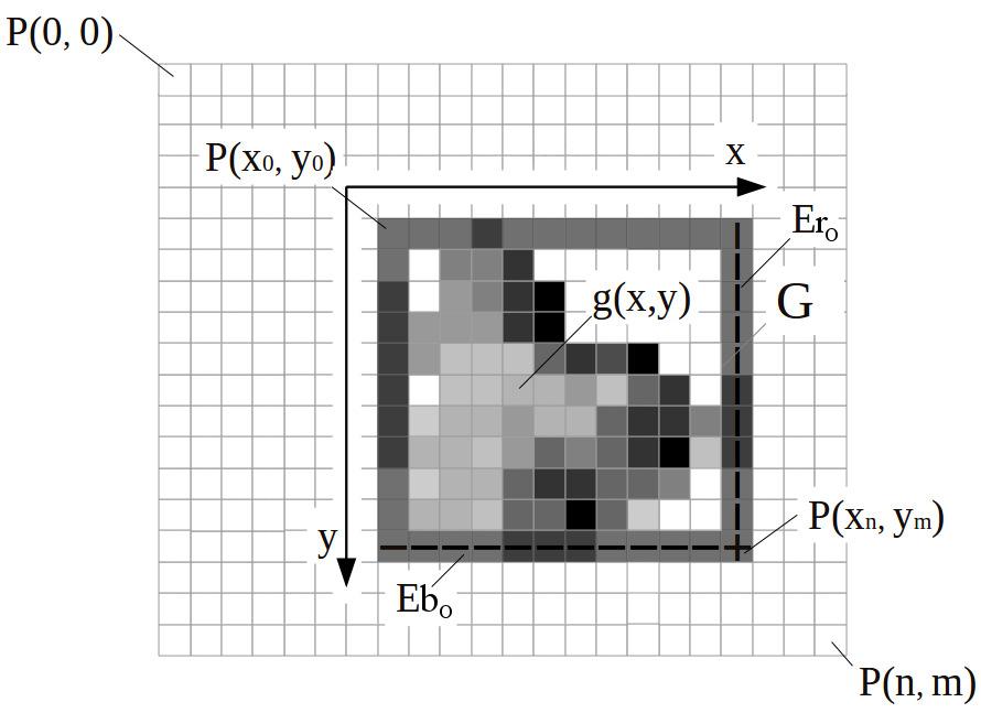
The edges of the bounding box span a local cartesian coordinate system separately for each object which is also called the Local Calculation Area of the object (see Figure 4). The rightmost x-coordinate (ri) resp. the bottommost y-coordinate (bj) of the calculation area of an object O is then defined by:
ErO and Eb
are sets of all right edge pixels
respectively of all bottom edge pixels
which have to be computed by local 3x3 edge filters applying to the object's bounding box:
Figure 4 - Gray-scaled image object (O) enclosed by an object-related coordinate system denoted as local calculation area
143
w
,
,
() ( ) ()() ()()() () ∨∧∨ = = ++ ,. ;1 ,1,1 , , gPgPgPgPelse ifgP wP ijijijij ij Oij
() ( ) () () () () () () () () () () >∨>∧>∨> > = ++ ,0000 ,1 ** ,1 * ,1 * , * , * elsePgPgPgPg PgifPw ijijijij ij Oij (4)
( ){ (}) () {} ().1max ,1max , , == == OjOij OiOij bjjwP riiwP (5)
O
rij O P ,
OibjP , ,
( ){ } () {} 1: ,1: ,, ,, =∀= =∀= OO OO OibjOibj OrijOrij EbPiwP ErPjwP (6)
Signal & Image Processing : An International Journal (SIPIJ) Vol.2, No.3, September 2011
For gray-scaled images ri*O, bj*O, Er*O, Eb*O are defined in the same way using the g* function (2). The subsequent integer arithmetic computation steps are subdivided into forward and backward calculation. The forward calculation provides the zeroth and the first moments in x and y direction. During the backward calculation the centroid pixel emerges by evaluating the zeroth and the first moments.
3.3 Forward Calculation
Figure 5 - Distributed computation of the zeroth moment
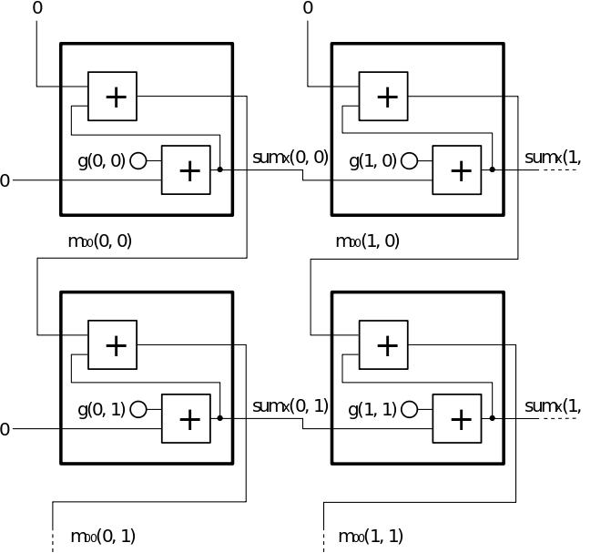
The mathematical derivation of the forward calculation in the case of binary images, including the distributed computation of the zeroth (m00) and the first moments in horizontal (m01) and vertical direction (m10), is already described in [21] and [19]. For gray-scale images the binary pixel value g(P) has to be replaced with g*(P). Figure 5 shows the scheme to cumulate the zeroth moment sum (object mass) beginning from the upper left towards the bottom right edge.
3.4 Backward Calculation
To avoid area consuming division operators, the backward computation process is distributed in a similar way as shown in Figure 5. The two-dimensional topology can be easily used to substitute the division by successive subtractions. For this purpose, the backward calculation process (here only shown for the y-coordinate) starts with the initialization of two CU-registers in the bottom right pixel nmOP , of the local calculation area. The registers are denoted as n (numerator) and d (denominator):
Furthermore, all edge state registers ey(i,j) receive a logical 1, if j = n.
Note 1. The content of register d is equal for both, the x- and y-coordinate. Therefore, no index is required.
Finally, the pixel nmOP , is left and has to be successively shifted into the object's center. In fact it virtually "marches" into the centroid, while carrying the registers ny (resp. nx) and d. The values of these registers are changed in the following way, depending on their actual position (i,j):
144
() (,)(,),,(),(). (,)(,) 00 10 OO y ifPijErPijEbdnmmnm nnmmnm ∈∧∈ = = (7)
Vol.2, No.3,
3.5 Centroid Detection
The CU-register midy(i,j) is set to a logical 1 or 0, if the following conditions occur:
else
(10)
In the case of a logical 1, midy(i,j) respectively the corresponding pixel P(i,j) is located at the ycoordinate of the center of mass axis.
Note 2. The backward calculation in x-direction is carried out on exactly the same way, only the coordinate label has to be changed. The centroid is determined by a logical AND of midy(i,j) and midx(i,j): ,(),(),() midijmidijmidij yx
(11)
In fact, the centroids mid(i,j) are binary result pixels located in a cartesian coordinate system (denoted as "centroid image") as well as the origin data. A step-by-step computation example of an object with a calculation area of 4x4 pixels can be found in [20].
4. IMAGE PRE PROCESSING
4.1 Parallel Full Buffering Scheme
The FB approach is frequently rejected because of its higher resource consumption. The problem is that several complete rows have to be buffered internally in queues (shift registers). For a comparison with a PB scheme often the Flip-Flops (FFs) and Look-up-tables (LUTs) of the FPGA are used for the implementation of the shift registers. But this is not an efficient implementation. In contrast, we recommend an implementation of the queues with the help of the FPGAs internal BRAMs (Block RAM). In today’s FPGAs, there are up to several hundred of these small memory blocks which can be efficiently concatenated to arbitrary sizes of data and address ports. By the use of BRAMs for the queue implementation, the overall resource consumption of a FB architecture can be greatly reduced.
As mentioned before, we have adapted the standard FB scheme to realize also a parallel processing of SWOs, if required, because often the image sensor frequency is higher than the system clock of the FPGA. There are also some image sensors which transfer the image data via more than one channel. Therefore, the degree of parallelization for the FB architecture in our system depends on the available pixels per system clock and can be adapted optimally.
Signal & Image Processing : An International Journal (SIPIJ)
September 2011 145 +++<+ += = . ,(,(),12,(,();1 (),,();1 ,() else nijdijifdijnij nijifeij nij yy yy y (8) + += = ,(),1. ,()(,1),,();1 dijelse dijdijifeij y (9)
< += = = ,12,(),(); ,()1 ,() ,()
ifnijdij ifnij ifdij midij y y y
=∧
Signal & Image Processing : An International Journal (SIPIJ) Vol.2, No.3, September 2011
Figure 6 - Full Buffering for parallel processing with p=2
Figure 7 - Full Buffering for parallel processing with p=4
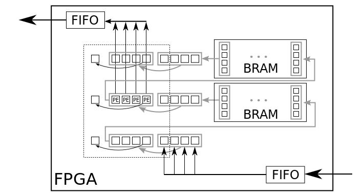
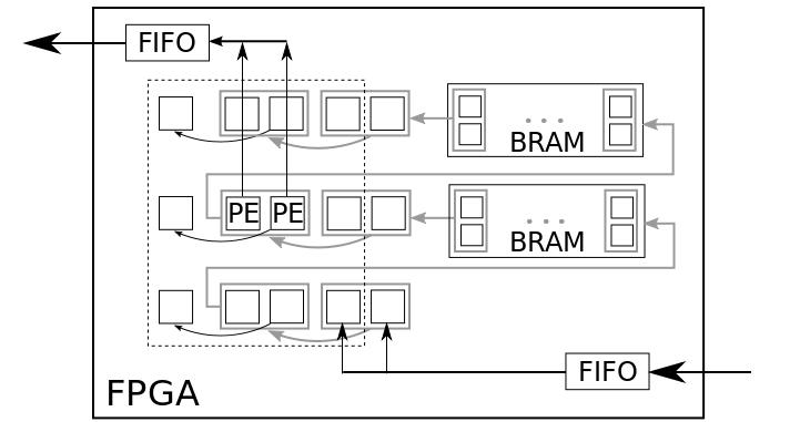
Our proposed architecture for a parallel processing with FB is outlined in Figure 6 for p = 2 and in Figure 7 for p = 4. As mentioned before, we used a fixed mask size of 3 × 3 pixels for the sliding window in our approach because it is sufficient for our field of applications. Every pixel, illustrated with small squares in the figures, contains a register for the storage of d bits. Some FIFO components can be integrated to compensate variations in the streaming process of the image data. In contrast to a standard FB approach, the shift width in our approach was adapted in order to realize a parallel processing. The shift width of the queues depends on the degree of parallelization p. This case is illustrated with gray boxes and gray arrows in the figures. Every gray box contains p pixels which are shifted within one clock cycle and there are p Processing Elements (PE) integrated for a parallel processing. Furthermore, the address and data ports of the BRAM components also depend on p. The black dashed box in the figures encloses all pixels required for the parallel SWO. The small squares on the left side of the dashed box are additional registers. Such a register preserves a right most pixel of a pixel block for the processing of the next pixel block. Every clock cycle, p new pixels are loaded from the image sensor, are processed and streamed to the Marching Pixel architecture, while shifting all buffered pixels with a shift width of p to the next pixel block location.
With this parallel FB processing approach a speedup of p compared to a standard FB implementation can be achieved with nearly the same resource consumption. The speedup is only constrained by the available pixels per system clock cycle. How this adapted FB scheme for a parallel processing can be used also for a pipelined processing of SWOs, will be presented in the following section.
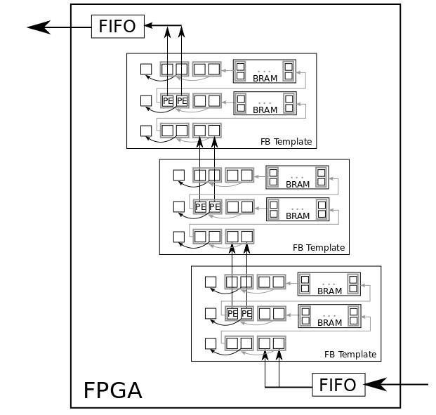
4.2 Pipelining of FB Stages
Because SWOs can be performed in a streaming fashion with an FB scheme, the result pixels of an FB stage can be directly fetched by further FB stages for the processing of further SWOs, before the image is sent to the Marching Pixel architecture. Hence, with our processing approach, a pipelining of FB stages is possible to process different image pre-processing operations based on SWOs simultaneously, with a marginal latency overhead per stage. In the following, we use the parameter it for the designation of the number of pipelined instances of our FB architecture for parallel processing and, hence, the number of simultaneously processed SWOs. The pipelining is illustrated for p = 2 and it = 3 in Figure 8.
146
Image Processing : An
(SIPIJ) Vol.2, No.3,
Figure 8 - Pipelining of FB Stages
Because every FB stage has to be initialized, an overhead of (mp + 2) clock cycles is required for every instance, where mp = m/p, before the first image pixels can be processed by the PEs. The greater the degree of parallelization is, the smaller is the number of clock cycles required for initialization. Therefore, a speedup of almost (p·it) is feasible for all performed image preprocessing operations.
4.3 FPGA Implementation
For the realization of this new parallel and pipelined FB scheme, we implemented a generic VHDL template for FPGAs and tested it on Spartan3E-1200 from the Xilinx. When using our template, the parameters m and n for the image resolution, d for the bits per pixel, p for the degree of parallelization and it for the pipeline depth have to be adapted. Furthermore, the PEs have to be specified in VHDL to realize the SWOs which should be performed. A problem which has to be solved in conjunction with SWOs, is the handling of the border pixels of the image. We made the handling of border pixels selectable for our VHDL template. The border pixels can be set to fixed values, but also an overlapping for the realization of a torus topology is possible. Therefore, the interface of a PE contains, beside the pixel information of the sliding window, also a signal which notifies if the current processing position is in the border region or not. In the current version of the VHDL template, the mask size for the SWOs is fixed to 3x3 pixels which is sufficient for the applications here. Currently, we improve the template to allow SWOs with arbitrary sizes.
As mentioned before, we implemented and tested the VHDL template for a Spartan3E-1200 FPGA. To show the flexibility of our architecture, we implemented some binary and also some gray-scale operations for the input object image of Figure 1 which is shown in more detail in Figure 9. For testing purposes, we used here only a small resolution of 128x128 pixels. In Figure 10, the binarized version of this image can be found which can be realized with Equation (1). A problem which is shown in Figure 10 are distortions and noise in the binarized version of the input image. This can lead to failures in the Marching Pixel processing, e.g. in the object centroid determination. Especially noise pixels at the image background can lead to failures by the object centroid determination with Marching Pixels. With the help of our template, the image content can be enhanced in the FPGA by remove noise or distortions with image preprocessing operations based on SWOs. It is also possible to transform gray-scale images if required.
Signal &
International Journal
September 2011 147
The reduction of noise of the objects in a binarized image with our template is illustrated in Figure 11. We used a 6-stage pipeline to perform Dilatation and Erosion operations for the realization of Open (Erosion followed by a Dilatation operation) und Close (Dilatation followed by a Erosion) operations. The result shown in Figure 11 was calculated by a Close operation to reduce object distortions, followed by a two times Open operation to reduce noise at the image background. Figure 12 shows an example of an gray-scale image transformation on the input image with the help of our template. We used a 2-stage pipeline where in the first FB stage a Median filter is applied on the gray-scale input image to reduce noise. The second FB stage realizes a Sobel filter which can be used for edge detection in gray-scale images.

We implemented and tested these two examples on a Nexys2 board from Digilent which contains a Spartan3E-1200 FPGA from Xilinx. The FPGA contains 8672 Slices, 17344 FFs and 28 18KbBRAMs (Block RAM). For testing purposes, we can transfer images via a serial interface to the FPGA and after the processing of the image with our FB pipeline it is displayed on a external monitor which is connected to the VGA interface of the board. In the following, we will present some synthesis results of our VHDL template which consists of the FB pipeline and a control unit. We used a significiant image resolution of n = m = 1024 pixels. In Table 1 the synthesis results of the template pipeline for the Open/Close operations are shown. For these operations only binary images are required, this means d = 1 and we used a 6-stage pipeline which means it = 6 for this example. In Table 2 the synthesis results of the template pipeline for the Median/Sobel filter on gray-scale input images are shown. For this example d = 8 and a 2-stage pipeline was used which means it = 2 for this example.
 Signal & Image Processing : An International Journal (SIPIJ) Vol.2, No.3, September 2011
Figure 9 - Gray-scale image from sensor Figure 10 - Binarized version of the input image
Figure 11 - Noise reduction by Open/Close Operations on the binarized input image
Figure 12 - Image transformation by applying a Median filter followed by a Sobel filter
Signal & Image Processing : An International Journal (SIPIJ) Vol.2, No.3, September 2011
Figure 9 - Gray-scale image from sensor Figure 10 - Binarized version of the input image
Figure 11 - Noise reduction by Open/Close Operations on the binarized input image
Figure 12 - Image transformation by applying a Median filter followed by a Sobel filter
148
Signal & Image Processing : An International Journal (SIPIJ) Vol.2, No.3, September 2011
Table 1 - Synthesis results for 6-stage Open/Close pipeline
Degree of parallelization p System frequency fmax Slices
FFs BRAMs
1 138 857 609 12
2 138 887 735 12
4 138 910 795 12
8 138 1067 1053 12
Table 2 - Synthesis results of a 2-stage Median/Sobel filter pipeline
Degree of parallelization p System frequency fmax
Slices
FFs BRAMs
1 56 948 673 4
2 56 1177 831 4
4 55 1619 1149 4
8 55 2569 1787 8
Both examples show the flexibility of our special buffering pipeline for image pre-processing operations. A lot of other SWOs could be implemented easily with the help of our VHDL template. As mentioned before, the input images are processed in a streaming fashion. The latency of this pre-processing depends mainly on the possible degree of parallelization and the pipeline depth and can be estimated with (mp+2)*it system clock cycles of the FPGA.
The synthesis results show that only a small amount of FPGA resources will be required for these image pre-processing operations. Hence, the FPGA could be used also for controlling purposes which are required in a stand-alone vision system, e.g. for controlling the image sensor or the Marching Pixel ASIC. After the enhancement or transformation of gray-scale or binarized input images, the Marching Pixel architecture can be used to perform MP algorithms like the Flooding algorithm for object centroid determination.
5.
MARCHING PIXEL CHIP ARCHITECTURE
5.1 Global Data Path
5.1.1 Binary image processing
The low pixel resolution (64x64) of the initial test chip design allows to read in the image data din in a line parallel fashion (see Figure 13). The local communication logic of CU cell enabled for binary pixel computation is attached at the right side of the figure. The chip operates in two global modes: either data input/output or data computation. The activity of the shift signal switches the chip to the input mode, where external image data is transferred and stored in the internal CU pixel registers.
Each CU-ALU cell contains one 1-bit register (denoted as DFF), in which the previously upper data value qpix/qmiddle state or the internal middle_state_i signal value can be stored, depending on the global mode state. In the case of an input image and a resulting centroid image identical in size, the read in / write out procedure can be carried out simultaneously. Therefore, one data register can be saved which leads to only one shared input/output DFF. During the read in phase, the signal shift is active, where each rising edge of the clock signal (clk) leads to a synchronous capturing of image data through the module Data_In_Control. The pixel registers are concatenated to a register chain leading to a vertical data transport from the upper to the lower edge of the CU array.
149
Signal & Image Processing : An International Journal (SIPIJ) Vol.2, No.3, September 2011
Figure 13 - Global datapath within CU-array, IO modules (gray)
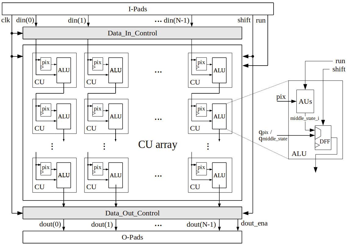
When the image capturing process is done, the signal run enables all CUs to read out the internal stored pix-value and to carry out the centroids (computation phase). After the computation latency has expired, the centroid image data are established at the AU's outputs. When releasing the global data communication path to its active state, the DFFs are chained again and the synchronous data output can occur via the Data_Out_Control unit by enabling the dout signal. At the same time new image data can be read in into the CU array.
5.1.2 Gray-scale image processing
To realize an easier global data communication, the gray-scale computation CU has separate data paths for the image and centroid data transport (see Figure 14). The single bit CU has to be replaced with the module, shown in Figure 14 which is able to process n-bit pixel values. The read in phase is characterized due to the storage of the n-bit image data into the pix-register. During the computation phase the stored bits rotate in counter-clockwise direction within the pix register. The internal ALU operands have deeper bit widths as the pixel operand. Therefore, a constant number of serial zero-bits have to be preceded, before the pixel's LSB can be computed. The number of the inserted bits depends on the pixel gray scale depth and the image resolution. If the computation of the centroids has be done, the procedure to output the centroid image is organized as explained above.
150
Signal & Image Processing : An International Journal (SIPIJ) Vol.2, No.3, September 2011
Figure 14 - Local datapath within a gray-scale pixel computing CU
5.2 Local data path
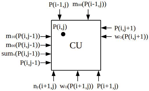
The local data path of the MP architecture is characterized by orthogonal serial data connections between the CUs. In Figure 15 a CU black box representation is shown. The figure depicts all neighboured input data to compute the y-coordinate of the object's centroid. For more details about the local datapath we refer to [3].
Figure 15 - Data Inputs for Flooding-CU
5.3 Prototype Chip
The physical implementation of the MP-Chip had been done for the binary image processing flow as described in subsection 5.1.1. The bit-serial working CU was designed only once, because after designing a CU chip layout it is reusable for any image resolution. The behavioral description of the entire chip is designed in a consistently generic way for both the vertical and the horizontal MP array resolutions n and m. Table 3 summarizes the layout results for one CU, one CU-line and the entire 64x64 MP chip design driven by a 50 MHz clock.
151
Signal & Image Processing : An International Journal (SIPIJ) Vol.2, No.3, September 2011
Table 3 - Layout parameters of the chip modules using a 90 nm CMOS technology
Parameter CU CU line Chip Ports
Inputs Data Control Outputs Data Control 18 6 12 640 6 768 64 4 64 1
Used metal layers Standard cells/marco blocks Gates 3 172 536 6 25/64 34413 7 767/64 2207516
Physical dimensions
Height/µm Width/µm 41.22 41.60 45.14 2755.00 3636 3424
Critical Path latency/ns 1.48 2.59 9.67
In Figure 16 the resulting prototype chip is shown as a GDSII database representation. The squared chip core is formed by 64x64 MP calculation units. The pad ring consists of the data inand output pads (64 pads each) located at the top and bottom chip edge. The left and right pad ring segments contain eight pairs of core power supply pads (four each).
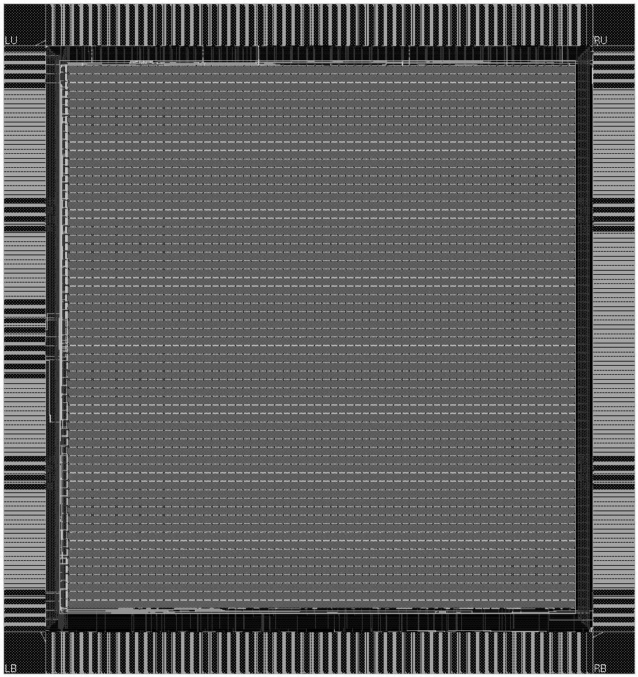
Figure 16 - Chip prototype layout (without bonding pads)
5.4 Benchmark comparison
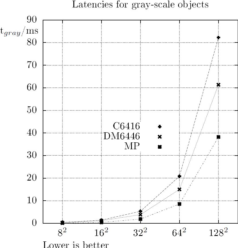
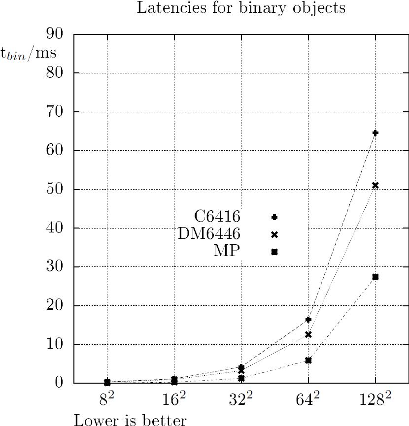
To demonstrate the performance of chip architectures derived from our MP design strategy, a comparison with simulation results of two different TMS320 DSP platforms had been carried out. The older C6416 as well as the actual DaVinci platform (DM6446) had been simulated at a virtual CPU clock of 500 MHz. Therefore, a software benchmark running on the DSP cores models has been created by manually optimized C code programming. The computation of centroids bases on projections of binary and gray-scale image objects (with a bit-width of eight), where the algorithmic approach is similarly to [13]. In addition to the absolute worst case latencies shown in Figure 17, the achieved speedups (Figure 18) are plotted as a function of squared worst case object resolutions N2. The MP-algorithm's worst case is the largest possible L-shaped image object with a width of exactly one pixel. As shown in the figures, a speedup of up to eight can be achieved with the MP ASIC compared to the used medium DSP platforms.
152
Signal & Image Processing : An International Journal (SIPIJ) Vol.2, No.3, September 2011

6. CONCLUSION
This paper depicts an processing pipeline for embedded image processing systems based on Marching pixels. An efficient buffering strategy for the realization of image pre-processing operations in a low-power FPGA, to enhance the captured images for the Marching Pixel architectures, was presented. We illustrated, how several image pre-processing operations can be realized with an adapted full buffering scheme in a parallel and pipelined fashion. Furthermore, we explained the Marching Pixel architecture as well as the design strategy to realize a Marching Pixels prototype chip in detail. The Marching Pixels concept is an alternative design paradigm to determine global image information, like centroids of objects, in an elegant fashion using a dedicated hardware platform. We showed, that an array of simple structured hardware modules is able to extract centroids of image objects of any shape and size faster than commonly used DSP platforms. We denote that the benchmark comparison results are based on a serial data input and the largest possible worst case object, depending on the MP array resolution. The computation latencies decrease dramatically using the line-parallel data input scheme supported by our chip architecture and several image objects with smaller form factors than the worst case object.
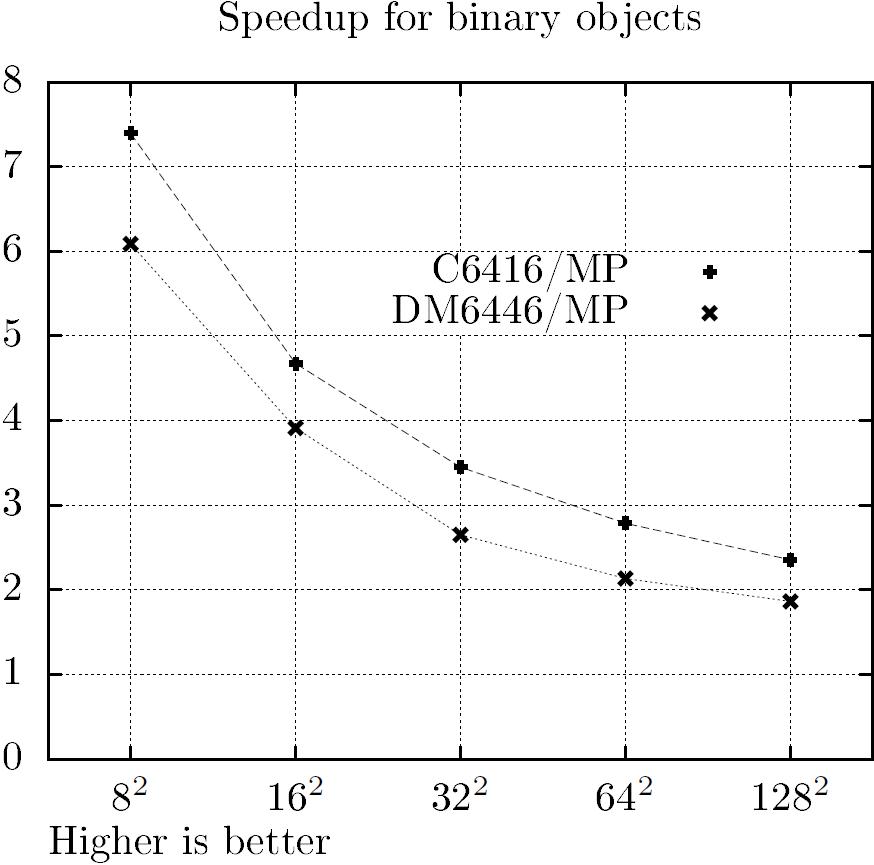 Figure 17 - MP-latencies vs. DSP-benchmarks for squared worst case objects
Figure 18 - Speedups for squared worst case objects
Figure 17 - MP-latencies vs. DSP-benchmarks for squared worst case objects
Figure 18 - Speedups for squared worst case objects
153
Signal & Image Processing : An International Journal (SIPIJ) Vol.2, No.3, September 2011
Together, both presented architectures can be used to build up a processing pipeline for standalone machine vision systems utilizing Marching Pixel approaches.
ACKNOWLEDGEMENTS
The work was partially supported by funding from the Application Centre from the Embedded Systems Initiative, a common institution of the Fraunhofer-Institute for integrated circuits and the Interdisciplinary centre for Embbeded Systems (ESI) at Friedrich-Alexander-University ErlangenNuremberg supported by the Bayerisches Staatsministerium für Wirtschaft, Infrastruktur, Verkehr und Technologie
REFERENCES
[1] T. Bräunl, Parallel Image Processing. Berlin, Germany: Springer-Verlag, 2000.
[2] L. T. Yang and M. Guo, High-performance computing:paradigm and infrastructure, ser. Wiley Series on Parallel an Distributed Computing, A. Y. Zomaya, Ed. Wiley-Interscience, 2005.
[3] A. Loos, M. Reichenbach and D. Fey, “ASIC Architecture to Determine Object Centroids from GrayScale Images Using Marching Pixels,” Advances in Wireless, Mobile Networks and Applications, vol. 154, pp. 234–249, 2011.
[4] X. Liang, J. Jean, and K. Tomko, “Data buffering and allocation in mapping generalized template matching on reconfigurable systems,” The Journal of Supercomputing, vol. 19, no. 1, pp. 77–91, 2001.
[5] X. Liang and J. S.-N. Jean, “Mapping of generalized template matching onto reconfigurable computers,” IEEE Transactions on Very Large Scale Integration (VLSI) Systems, vol. 11, pp. 485–498, 2003.
[6] F. Cardells-Tormo and P.-L. Molinet, “Area-efficient 2-d shift-variant convolvers for fpga-based digital image processing,” IEEE Transactions on Circuits and Systems II: Express Briefs, vol. 53, no. 2, pp. 105–109, 2006.
[7] M. Javadi, H. Rafi, S. Tabatabaei, and A. Haghighat, “An area-efficient hardware implementation for real-time window-based image filtering,” in Third International IEEE Conference on Signal-Image Technologies and Internet-Based System, 2007, pp. 515–519.
[8] H. Zhang, M. Xia, and G. Hu, “A multiwindow partial buffering scheme for fpga-based 2-d convolvers,” IEEE Transactions on Circuits and Systems II: Express Briefs, vol. 54, pp. 200–204, 2007.
[9] H. Yu and M. Leeser, “Automatic sliding window operation optimization for fpga-based computing boards,” Annual IEEE Symposium on Field-Programmable Custom Computing Machines, vol. 0, pp. 76–88, 2006.
[10] C. Torres-Huitzil and M. Arias-Estrada, “Fpga-based configurable systolic architecture for windowbased image processing,” EURASIP Journal on Applied Signal Processing, vol. 7, pp. 1024–1034, 2005.
[11] D.L. Standley, “An object position and orientation ic with embedded imager,” IEEE Journal of SolidState Circuits, vol. 26, pp. 1853–1859, 1991.
[12] Y. Watanabe, T. Komuro, S. Kagami and M. Ishikawa, “Parallel extraction architecture for information of numerous particles in real-time image measurement,” Journal of Robotics and Mechatronics, vol. 17, no. 4, pp. 420–427, 2005.
[13] F. Schurz and D. Fey, “A programmable parallel processor architecture in fpgas for image processing sensors,” Integrated Desgin & Technology, Society for Design and Process Science, 2007
[14] G. Costantini, D. Casali and R. Perfetti, “A new cnn-based method for detection of symmetry axis,” 10th International Workshop on Cellular Neural Networks and Their Applications, pp. 1–4, 2006.
154
Signal & Image Processing : An International Journal (SIPIJ) Vol.2, No.3, September 2011
[15] P. Dudek and M. Geese, “Autonomous long distance transfer on simd cellular processor arrays, ” 12th IEEE International Workshop on Cellular Nanoscale Networks and Their Applications, pp. 1–6, 2010.
[16] D. Fey and D. Schmidt, “Marching pixels: a new organic computing paradigm for smart sensor processor arrays,” Second Conference on Computing Frontiers, pp. 1–9, 2005.
[17] M. Komann and D. Fey, “Marching pixels - using organic computing principles in embedded parallel hardware,” International Symposium on Parallel Computing in Electrical Engineering, pp. 369–373, 2006.
[18] D. Fey, M. Komann, F. Schurz and A. Loos, “An organic computing architecture for visual microprocessors based on marching pixels,” IEEE International Symposium on Circuits and Systems, pp. 2686–2689, 2007.
[19] M. Komann, A. Kröller, C. Schmidt, D. Fey and S.P. Fekete, “Emergent algorithms for centroid and orientation detection in high-performance embedded cameras,” Conference on Computing Frontiers, pp. 221–230, 2008.
[20] D. Fey, C. Gaede, A. Loos and M. Komann, “A new marching pixels algorithm for applicationspecific vision chips for fast detection of objects' centroids,” Parallel and Distributed Computing and Systems, 631-805, 2008.
[21] C. Gaede, “Vergleich verteilter algorithmen für die industrielle bildvorverarbeitung in fpgas,” Master's thesis, Friedrich-Schiller University Jena, Germany, 2007.

Authors
Michael Schmidt received his diploma degree in computer science in 2005 from the University of Jena, Germany. From 2005 to 2009 he was a member of the research staff at the Chair of Computer Architecture at University of Jena. Since 2009 he is working at the Unversity of ErlangenNuremberg, Germany. His main research interests are embedded systems and FPGAs. He is currently working on efficient FPGA hardware architectures for image processing and robotics.
Marc Reichenbach studied Computer Science at University Jena, Germany. Since 2010 he is working at University Erlangen-Nuremberg, Germany, as a member of the research staff at the Chair of Computer Architecture. His main research interests are image processing in embedded systems, FPGA- and ASIC architectures and heterogeneous multi- and many-core architectures.
155
Signal & Image Processing : An International Journal (SIPIJ) Vol.2, No.3, September 2011
Dr. Ing. Andreas Loos, born in 1972 in Germany, studied Electrical Engineering at the University of Applied Sciences Jena. He graduated as Dipl.-Ing. (FH) in 2000. During a postgraduate course in technical computer science at Friedrich Schiller University Jena he worked on projects to develop and to integrate highly parallel digital image processing algorithms in ASIC hardware. His later research work focused on the integration of biological inspired algorithms to extract global object features in images. In 2011 he received his PhD in Computer Science from the Friedrich Schiller University Jena. Since Spring 2011 he works at TES Electronic Solutions GmbH in Munich, Germany.

Prof. Dr. Ing. Dietmar Fey studied computer science at the University Erlangen-Nuremberg. The topic of his PhD thesis in 1992 was about Optical Computing Architectures. From 1999 to 2001 he was researcher and lecturer at the Universities Jena and Siegen in Germany. In 2001 he became a professor for Computer Engineering at the University of Jena. Since 2009 he has the Chair of Computer Architecture at the University of Erlangen Nuremberg, Germany. His research interests are in the areas of parallel embedded processor architectures, heterogeneous parallel architectures, Cluster and Grid computing and Nanocomputing.

156