
COMPARISON OF GPU AND FPGA HARDWARE ACCELERATION OF LANE DETECTION ALGORITHM
Mohamed Alshemi1, Sherif Saif2 and Mohamed Taher3
1Computer and Systems Engineering Department, Ain Shams University, Cairo, Egypt
1STMicroelectronics, Cairo, Egypt
2 Computer and Systems Department, Electronics Research Institute, Cairo, Egypt
3 Computer and Systems Engineering Department, Ain Shams University, Cairo, Egypt
ABSTRACT
The two fundamental components of a complete computer vision system are detection and classification. The Lane detection algorithm, which is used in autonomous driving and smart vehicle systems, is within the computer vision detection area. In a sophisticated road environment, lane marking is the responsibility of the lane detection system. The warning system for a car that leaves its lane also heavily relies on lane detection. The two primary stages of the implemented lane detection algorithm are edge detection and line detection. In order to assess the trade-offs for latency, power consumption, and utilisation, we will compare the state-of-the-art implementation performance attained with both FPGA and GPU in this work. Our analysis highlights the benefits and drawbacks of the two systems.
KEYWORDS
Lane Detection, Computer Vision, FPGA, GPU, CUDA
1. INTRODUCTION
Lane detection has long been a significant issue with driver assistance systems (ADAS). Lane detection, the initial stage of road segmentation, makes it easier for autonomous vehicles to comprehend the scene. For instance, many automotive features like lane departure warning (LDW), adaptive cruise control, lane centring, and lane change assist require lane detection. In recent years, there have been some improvements made to the lane detecting problem.
Power consumption can be considerable to achieve real-time performance in a lane detection solution because of the computational complexity of the lane detection method. Even while power consumption isn't a factor in every design, low power options are frequently needed for embedded or edge computing solutions. Graphical processing units (GPUs) were formerly used to process computationally difficult images, but because to advancements in field programmable gate array (FPGA) technology, these tasks are now more practical with FPGA devices that use less power
So through this paper, two lane detection hardware implementation solutions are developed and compared. One solution is implemented on a ZYNQ-7 ZC706 Evaluation Board FPGA [1] and the other solution is implemented on Google Colab NVidia K80 Super GPU [2]. The implementation for both FPGA and GPU will be shown in Figure 1
Signal & Image Processing: An International Journal (SIPIJ) Vol.13, No.6, December 2022
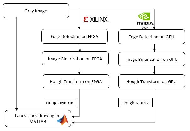
The implementation includes the following steps.
Step 1: Sobel edge detection for a gray image.
Step 2: Applying the image binarization.
Step 3: Obtaining the Hough matrix as a result of the Hough transform.
Step 4: MATLAB functions are used to process the Hough matrix to draw the lane lines.
2. THE ALGORITHM EMPLOYED FOR LANE DETECTION
Lane detection is divided into three parts [3].
2.1. Sobel Edge Detection
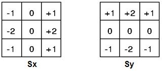
In order to extract features from images, such as edges, the Sobel edge detection technique is utilised [4]. It works by figuring out the gradient of image intensity for each pixel in the image. The output indicates how abruptly or gradually the image changes at each pixel, and consequently, how much that pixel resembles an edge. It also indicates how that edge is oriented. It detects the direction with the largest change from light to dark and the change rating in that direction. A vector that transitions from darker to brighter values across an edge is produced when a Sobel filter is applied to a pixel on the edge
According to Figure 2, the Sobel filter employs two 3 x 3 matrix kernels. With one, changes in the horizontal direction are calculated, and with the other, changes in the vertical direction. The derivative approximations are calculated by convolving the two kernels with the initial grayscale pixel image. Where the approximated magnitude is
2.2. Image Binarization
Binarizing images before further processing is the objective of this method. After that, every pixel in the image will either be 255 or 0. (A pixel is normally represented by 8 unsigned bits, making 255 the highest value in the 8-bit data format)
2.3. Hough Transform
The Hough transform is used to determine the two lines of the lane after image binarization [4]. The Hough transform is the most crucial method for identifying forms in pictures. It has been used particularly to extract random shapes like circles, lines, and squares. In other words, the Hough transform algorithm is the best approach for line identification because it has been acknowledged as a promising method for shape and motion analysis in images [5]. A line is represented by the following equation:
In [r, ] coordinates, a line can be:
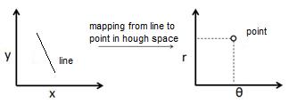
Where parameter is the angle of the line, and parameter r is the distance from the line to the origin. Thus, the line can be represented by a single point of Polar (r, ) coordinate in Hough space. In this way, a line in the Cartesian (x, y) coordinate system can be mapped to a single point in (r, ) Hough space, as indicated in Figure 3.
Signal & Image Processing: An International Journal (SIPIJ) Vol.13, No.6, December 2022
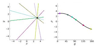
Conversely, a point in the (x, y) coordinate system represents all lines passing through that point. This way a point maps all possible lines that pass through it in Hough space. As shown in Figure 4, a point maps to a line that looks like a sinewave in the Hough space [5].
Each point in the binarized generated image votes to its corresponding possible lines, which are pairs of (r, Ө) in Hough space, in order to identify straight lines inside an image. An accumulator array is created after each pixel in the input image has been processed. The line with the highest count value is the one with the greatest number of pixels on it. The process of picking the line with the most pixel value is called Hough Peak which is done in Matlab.
3. HARDWARE IMPLEMENTATION ON FPGA
3.1. Sobel Edge Detection FPGA Implementation
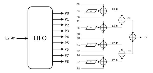
To ensure that the output image size is the same as the input image after receiving the grayscale image, the first step is to perform zero padding on the original image.
Figure 5 depicts a general architecture for computing kernel-based convolution. Adders and left shifters are used to implement the Sobel filter because its parameters only have three possible forms: 1, 2, and 0.
Hardware resource usage can be decreased by replacing multipliers with left shifting by 1 to realise multiplication by 2 (Area optimization).
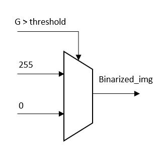
3.2. Image Binarization FPGA Implementation
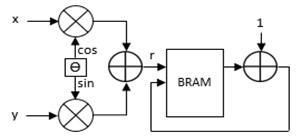
Image binarization on hardware is implemented by using a multiplexer and an unsigned comparator as shown in Figure 6.
3.3. Hough Transform FPGA Implementation
After Image binarization, lines from all possible directions are counted for every pixel that is equal to 255. The range of the line angles is [0, 180], and each angle's distance from the origin is calculated using the structure depicted in Figure 7, which may be thought of as the basic processing component of the Hough transform. Since there is a degree resolution of one degree between angles, 180 of these processing pieces are required to compute over a range of 180 degrees. Each processing element's output is counted up and stored in memory [6].
Figure 7 demonstrates that each processing element cell requires two multipliers, and since there are 180 of these processing elements used, a total of 360 multipliers are required. By modifying the sine and cosine functions' characteristics, we further improve the use of multipliers [7]. The following equations provide expression to such features:
Where Ө1 + Ө2 = 180, sin (Ө1) = sin (Ө2), and cos (Ө1) = -cos (Ө2). In other words, once sin (Ө1) and cos (Ө1) are calculated, sin (Ө2) and cos (Ө2) can be done by simple add/minus operations. In this way, only 180 multipliers are used instead of 360, saving 50% of the total number of multipliers.
4. HARDWARE IMPLEMENTATION ON GPU
Our GPU implementation was based on Google Colab NVidia Tesla K80 Super GPU connected to a host CPU via PCIe. The GPU has 4992 NVIDIA CUDA cores with a base clock of 562 MHz it has 12GB global memory operating on a memory clock of 1253 MHz CUDA was used to program the GPU.
With less modifications to C, NVidia's Compute Unified Device Framework (CUDA) offers a general architecture for GPUs that enables flexible programming. CUDA’s view of a GPU has plentiful Streaming Multiprocessors. Each multiprocessor has a shared memory which is a fast local memory shared by its streaming processors. All multiprocessors also have access to a global or device memory. A thread block can be formed by many threads on a streaming multiprocessor. A thread block maps to a Streaming Multiprocessor physically although the threads number inside a block can be bigger than the number of Streaming processors, in which case threads are split into multiple warps where only one warp is active at a time. Active threads can execute the same instruction in parallel.
The components of the Lane Detection must be carefully mapped to the GPU computing architecture in order to make optimum use of GPU computing resources and to reduce the access cost of device memory access.
Two principles guided our mapping:
1. Avoid unnecessary device memory access and prefer shared memory for repeated memory access and
2. Avoid branches to keep all the processors doing useful computation work.
Currently available GPUs have a limited amount of shared memory per multiprocessor, with the majority of them providing roughly 48KB of shared memory per block [8].
4.1. Sobel Edge Detection GPU Implementation
After receiving the gray image, we start with doing the zero padding for the original image and store it inside the device memory then we use a 2D grid which contains a 2D Block with a size of 16*16 threads, as in the following equation
Where width and height are the dimensions of the original gray image. Each block will perform the Sobel operator convolution on the gray image and all the grid blocks will perform the computations in parallel.
4.2. Image Binarization GPU Implementation
Each block thread will be responsible for the threshold of the post-Sobel pixels to be 255 or 0.
4.3. Hough Transform GPU Implementation
The Hough transform voting space (r, ) is divided into partitions for each and the voting method for each partition is performed concurrently. A thread block in the GPU implementation [9], is assigned to each where threads in the thread block concurrently vote for input postbinarization pixels. Partitioning the voting space for each where each voting space can be stored in the shared memory. Therefore, the voting mechanism is performed to the voting space in the block shared memory. In the GPU implementation, the voting space is partitioned into 180 spaces where thread blocks can vote in parallel. The values of the trigonometric functions cos and sin are initially computed in each thread block since the values are commonly used for every thread in a thread block. Then threads read the coordinates of input pixels stored in the global memory.
Some threads may vote to the same r simultaneously in the parallel voting procedure. To avoid it, we use the atomic add operation supported by CUDA [10].
5. EXPERIMENTAL RESULTS
The two systems’ performance was evaluated based on latency, power consumption, and resource utilization.
1- Latency was measured for both implementations between the first valid pixel of the image entering the system and the generation of the Hough Matrix.
2- Power was measured for both implementations as an average power using the devices’ specific tools.
Signal & Image Processing: An International Journal (SIPIJ) Vol.13, No.6, December 2022
3- Memory resource utilization for both implementations was measured for the Hough transform as BRAM memory in FPGA and shared memory in GPU.
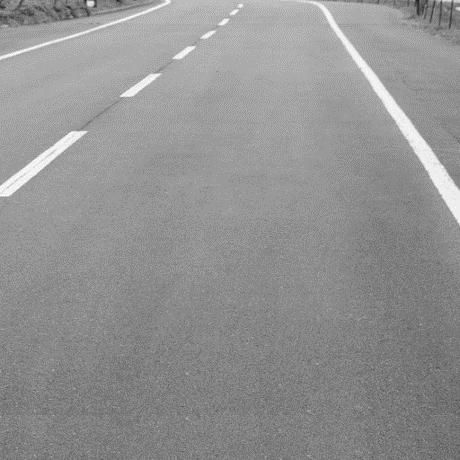
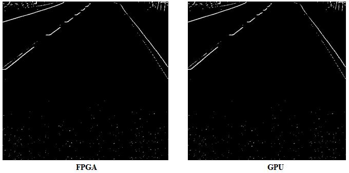
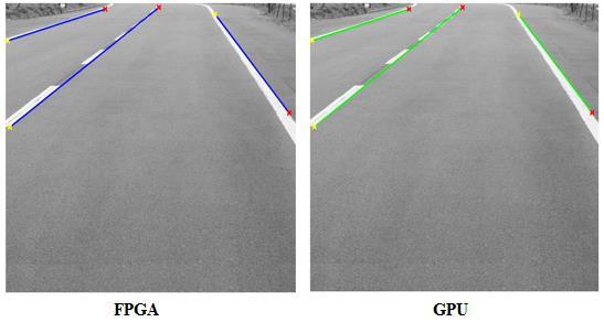
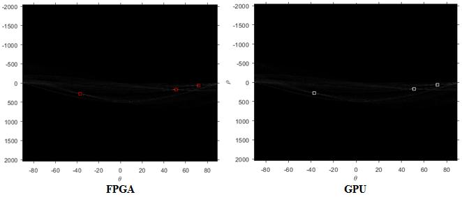
The results obtained for the proposed lane detection algorithm for the gray image in Figure 9 and the Sobel detection and binarization output for both implementations as in Figure 10. Some MATLAB built-in functions were used to detect the Hough peaks as in Figure 11. For the Hough Matrix generated from both FPGA and GPU and Hough lines as in Figure 12 to draw the lane lines.
Table 1 shows the resource utilization of the Lane Detection Algorithm on ZYNQ-7 ZC706 Evaluation Board FPGA for 100 MHz frequency whereas Table 2 shows the performance comparison of the Lane Detection Algorithm between FPGA and GPU.
Signal & Image Processing: An International Journal (SIPIJ) Vol.13, No.6, December 2022
6. CONCLUSION
Two lane detection implementations were designed in this paper using two different types of hardware acceleration. Tests were performed out applying only the acceleration component of the lane detecting method, and the two types of hardware acceleration used were an FPGA and a GPU.
According to tests, FPGAs have low latency, whereas GPUs have low relative memory resource use. In terms of memory resource usage, GPUs handle resolution scaling equally well or better than FPGAs. In terms of latency, FPGAs handle resolution scaling equally well or better than GPUs. GPU is definitely a better option if your project will be implemented in this job and you need high resolution, which may be required later in the project. If performance and latency are critical and resolution may be limited, FPGAs are probably a better choice.
Finally, the results demonstrated that the FPGA outperformed the GPU in terms of latency, power consumption, and resource utilisation for [512x512] pixel images, but that the GPU handled resolution scaling better than the FPGA in terms of memory resource consumption.
7. FUTURE WORK
In future work, it would be beneficial to use canny edge detector instead of Sobel edge detector and analyze its effect on the performance of the output image after the edge detection.
REFERENCES
[1] Xilinx Inc, “ZC706 Evaluation Board for the Zynq-7000 XC7Z045 SoC User Guide (v1.8).” 2019.
[2] S. Mittal and J. S. Vetter, “A survey of CPU-GPU heterogeneous computing techniques,” ACM Computing Surveys, vol. 47, no. 4, pp. 1–35, 2015.
[3] C. Lee and J.-H. Moon, “Robust lane detection and tracking for real-time applications,” IEEE Transactions on Intelligent Transportation Systems, vol. 19, no. 12, pp. 4043–4048, 2018.
[4] R. C. Gonzalez and R. E. Woods, Digital Image Processing. Uttar Pradesh, India: Pearson, 2018.
[5] Y. Zhou, “Computer Vision System-On-Chip Designs for Intelligent Vehicles,” Ph.D. dissertation, UC Davis, 2018.
[6] D. Northcote, L. H. Crockett, and P. Murray, “FPGA implementation of a memory-efficient Hough parameter space for the detection of lines,” 2018 IEEE International Symposium on Circuits and Systems (ISCAS), 2018.
[7] X. Zhou, Y. Ito, and K. Nakano, “An efficient implementation of the Hough transform using DSP slices and block rams on the FPGA,” 2013 IEEE 7th International Symposium on Embedded Multicore Socs, 2013.
[8] “Cuda C++ Programming Guide,” NVIDIA Documentation Center. [Online]. Available: https://docs.nvidia.com/cuda/cuda-c-programming-guide/index.html. [Accessed: 04-Nov-2022].
[9] S. Bagchi and T.-J. Chin, “Event-based star tracking via multiresolution progressive Hough transforms,” 2020 IEEE Winter Conference on Applications of Computer Vision (WACV), 2020.
[10] X. Zhou, N. Tomagou, Y. Ito, and K. Nakano, “Implementations of the hough transform on the embedded multicore processors,” International Journal of Networking and Computing, vol. 4, no. 1, pp. 174–188, 2014.