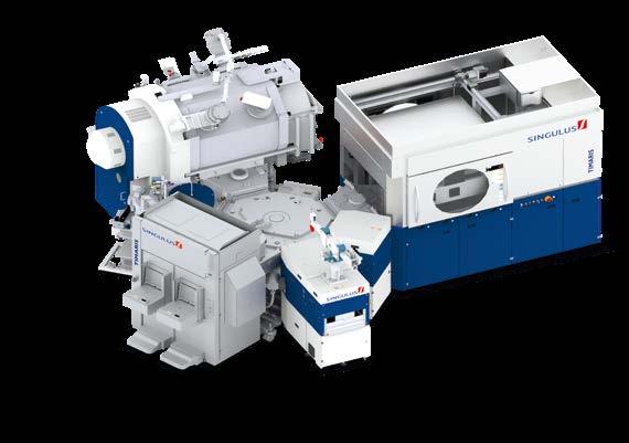
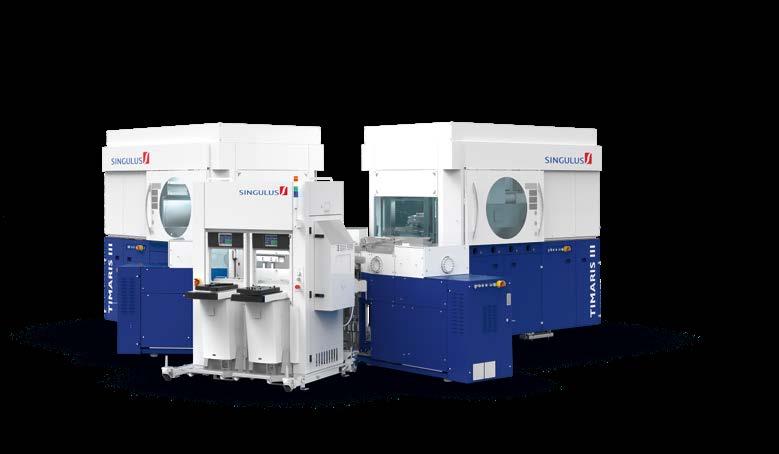
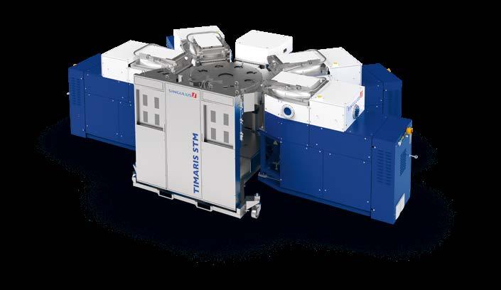
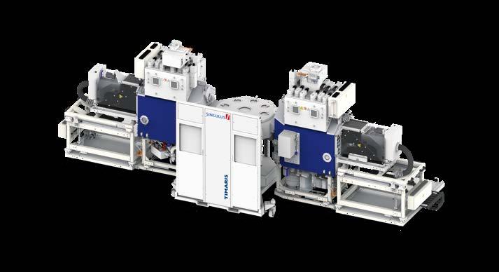
Example Configurations
(all configurations are available for 200 mm and 300 mm)
»
Applications:
Applications:
»
» Electrostriction application
Headquarters
SINGULUS TECHNOLOGIES AG Hanauer Landstrasse 103
63796 Kahl, Germany
Tel. +49 6188 440-0 sales@singulus.de www.singulus.com
Subsidiaries
China
SINGULUS TECHNOLOGIES (SHANGHAI) Co. Ltd.
Tel. +86 21
South America
SINGULUS TECHNOLOGIES
LATIN AMERICA LTDA.
Tel. +55 11 2165 2410 sales@singulus.com.br
South East Asia
SINGULUS TECHNOLOGIES
ASIA PACIFIC PTE LTD.
Tel. +65 67411912 sales@singulus.com.sg
Taipei Office
SINGULUS TECHNOLOGIES
TAIWAN LIMITED
Tel. +886 2 8692 6996 sales@singulus.com.tw
SINGULUS TECHNOLOGIES - Thin-Film Coating and Surface Treatment
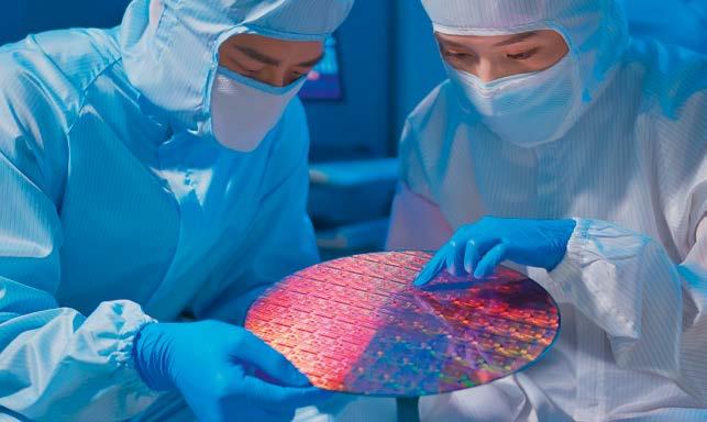
SINGULUS TECHNOLOGIES develops and assembles innovative machines and systems for efficient thin-film coating and surface treatment processes, which are used worldwide in the Photovoltaics, Semiconductor, Medical Technology, Packaging, Glass & Automotive as well as Battery & Hydrogen markets.
The company’s core competencies include various processes of coating technology (PVD sputtering, PECVD, evaporation), surface treatment as well as wet-chemical and thermal production processes.
SINGULUS TECHNOLOGIES sees sustainability as an opportunity to position itself with innovative products. In the focus are environmental awareness, efficient use of resources and avoidance of unnecessary CO₂ pollution.
SINGULUS TECHNOLOGIES attaches great importance to responsible and sustainable corporate governance.
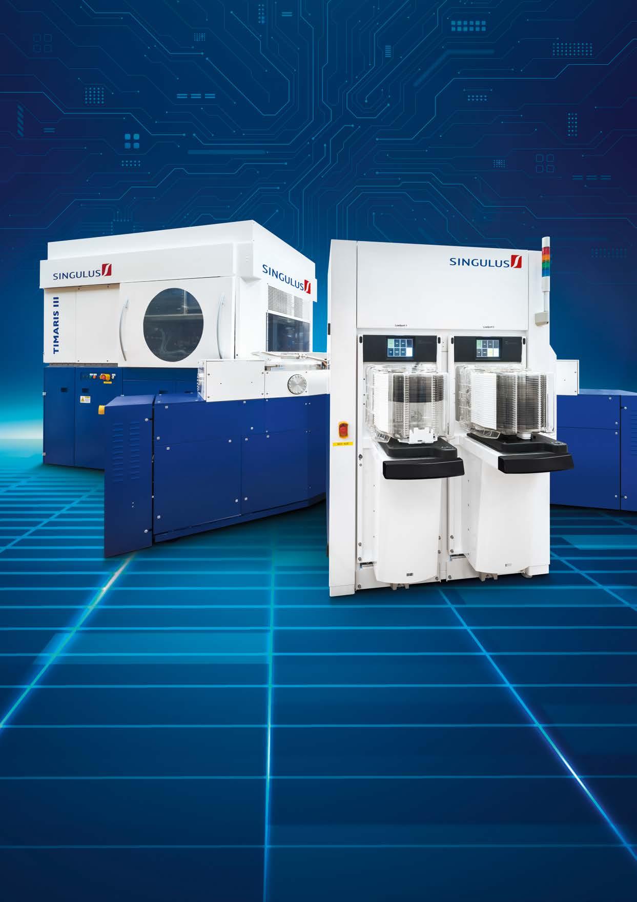
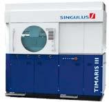
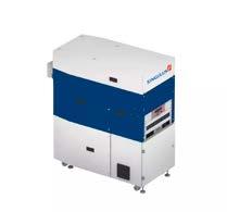
TIMARIS
Multi-Cathode Deposition Platform for Various Semiconductor, Advanced Packaging and Magnetic Applications
SINGULUS TECHNOLOGIES is a leading provider of cutting-edge vacuum deposition equipment, designed to meet the stringent requirements of semiconductor specialists. Our TIMARIS platform supports a wide range of thin-film deposition technologies, including sputtering, etching, as well as integrated heating and pre/post-processing steps.
Engineered for both front-end and back-end applications, our solutions deliver unmatched precision, reliability, and scalability for advanced semiconductor, packaging, and magnetic device production.
As a trusted industry partner, we continuously innovate to expand our capabilities and set new standards in thin-film deposition for next-generation technologies.
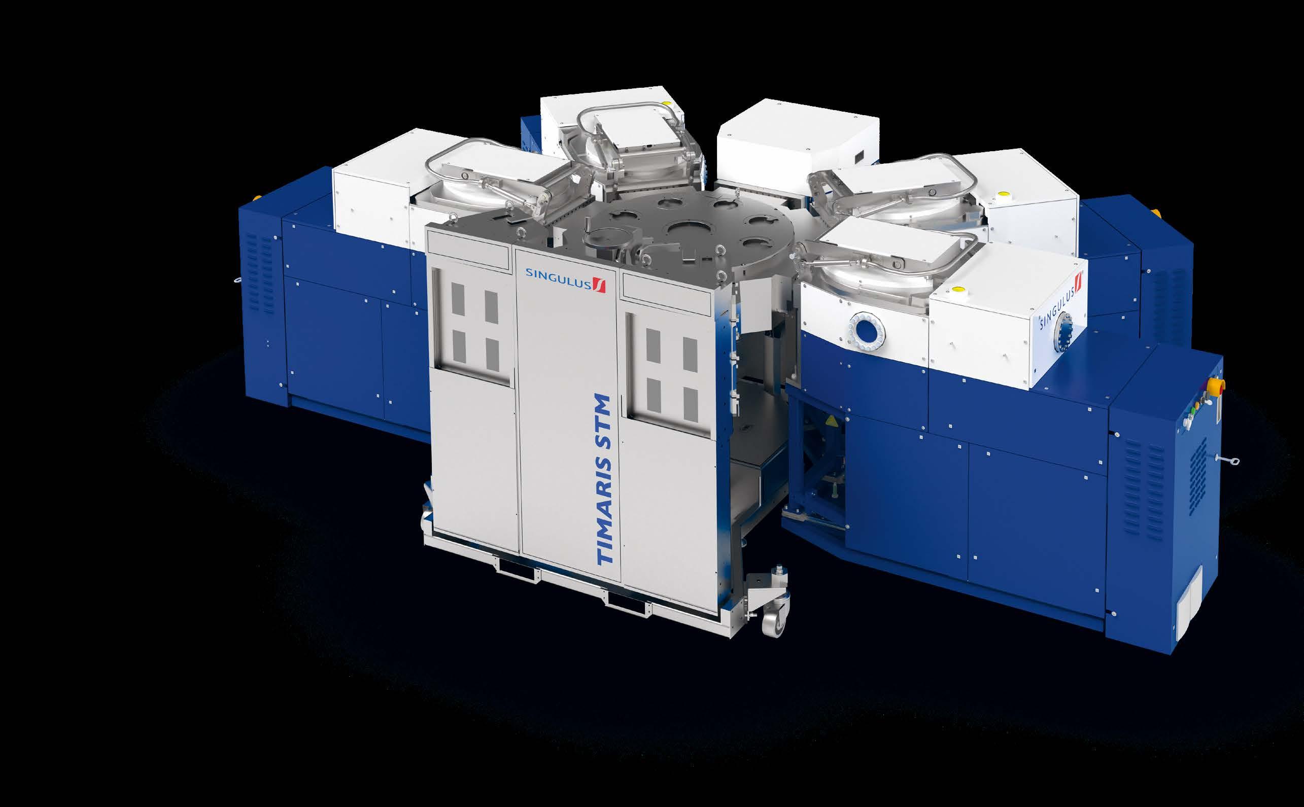
TIMARIS Cluster Tool System
The TIMARIS cluster tool platform addresses various semiconductor and magnetic applications.
Depending on the requirement, the cluster tool can be configured with different process modules which are optimized for each process.
The platform processes thicknesses ranging from a fraction of a nm up to several μm with a very precise control of the thicknesses and uniformities on the wafer.
All TIMARIS PVD modules incorporate the full scope of sputtering techniques such as:
DC magnetron, pulsed DC magnetron and RF magnetron sputtering as well as combinations of these modes that are selectable by recipe.
This allows the deposition of metallic and dielectric materials.
The TIMARIS cluster tool provides process features like:
» Multi-layer deposition
» Single layer deposition
» Co-sputtering of up to 4 targets
» Pre-clean combining Bias and ICP
» Plasma treatment/oxidation
» Heating
» Cooling
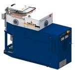
Multi-Target-Module with 10 DC/RF cathodes
The TIMARIS cluster tool perfectly fits to a wide range of applications for example:
» Magnetic sensors
» Integrated inductors
» Advanced packaging
» MRAM
» MEMS
» Thin-film heads
» μLED
» Power electronics
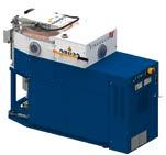
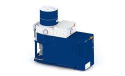
Four-Target-Module with 4 DC/RF cathodes
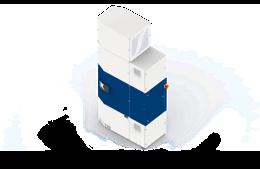
Rotating-Substrate-Module with 12 DC/RF cathodes Co-sputtering of up to 4 targets
MAIN CHARACTERISTICS
» High throughput for single layer and multilayer deposition
» Minimized break times for multilayer deposition
» Low cost of ownership
» Outstanding homogeneity due to the patented Linear Dynamic Deposition (Patent US 7,799,179)
» Excellent sub-Å thickness control with high repeatability
» Very long target life with optimized coating efficiency
» Qualified production processes
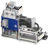
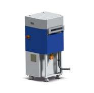
Single-Target-Module High-rate sputter deposition of metallic and non-conducting materials
Pre-Clean-Module Cleaning of wafer prior to deposition
ICP-Pre-Clean-Module Soft etching of wafer prior to the deposition
Oxidation-Process-Module Oxidation of wafer
Batch Thermal-Process-Module Parallel degassing of wafer batches
Thermal-Process-Module In-situ thermal processing of single wafers
Rapid-Cooling-Module Very fast cooling of the wafer down to -100 °C