SPUTTERING TECHNOLOGY
for Solar, Display, Glass, Semiconductor, Hydrogen, Decorative & Functional Coatings


for Solar, Display, Glass, Semiconductor, Hydrogen, Decorative & Functional Coatings
SINGULUS TECHNOLOGIES has delivered far more than 8,500 vacuum sputtering systems since its foundation in 1995. The machines range from ultra-high vacuum deposition equipment applying extremely thin layers of around 0.2 nm for the semiconductor industry down to highthroughput sputter machines for metallizing of small devices in 0.3 s.
PVD Systems from SINGULUS TECHNOLOGIES are mainly used in photovoltaics, data storage, sensor technology and decorative coatings but also in other applications such as hydrogen, battery, automotive, electrical shielding and advanced packing applications in the semiconductor industries.
A close cooperation with scientific institutes like Fraunhofer ISE, Helmholtz-Zentrum Berlin (HZB), and SERIS as well as with research organizations and institutes in Europe, the USA and Asia allow SINGULUS TECHNOLOGIES to participate and make use of the latest solar research results worldwide.
Well known sputtering methods are direct current (DC) sputtering for electrically conductive targets and radio frequency (RF) sputtering for nonconductive targets. Magnetron sputtering is available on the market in different modes like DC, pulsed DC, bipolar and RF. Due to its versatility, the convenient control of the process and the possibility to apply it on a large scale at low cost, sputter deposition or sputtering is widely used in different industries as well as in R&D applications.
» Over 8,500 sputtering devices worldwide
» Deposition systems for substrates larger than 2 m²

» In-house cathode design with magnetron development
» Simulation of sputtering processes with lab equipment in-house
» Software development
» Cooperation with scientific institutes in Europe, USA and Asia

» R&D department and lab dedicated to PVD and PECVD applications/activities
» Electrical and mechanical design department with high experience in thin-film technology and vacuum process technology

» Systems for vertical and horizontal substrate transport orientation
» Magnetron sputtering in diverse modes like DC, pulsed DC, bipolar and RF available
» Modular process chamber configuration
» Metals, oxides, nitrides and TCOs
» Reflector, contact, isolating and semiconductor layers
» Optical layers (AR, reflector)
» Protective layers (diffusion barriers, scratch resistant layers)
» Special magnetic layer stacks (spintronics, inductors etc.)
» Decorative coatings

» Antibacterial coating (e.g. Cu based)
» Thermal protection layers (low-E)
SINGULUS TECHNOLOGIES develops and assembles innovative systems and technologies for efficient and resource-saving production processes, which are used worldwide in the Photovoltaics, Semiconductor, Medical Technology, Packaging, Glass & Automotive as well as Battery & Hydrogen markets. The company’s core competencies include various processes of coating technology, surface treatment as well as wet-chemical and thermal production processes.

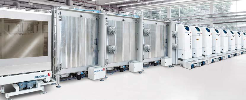
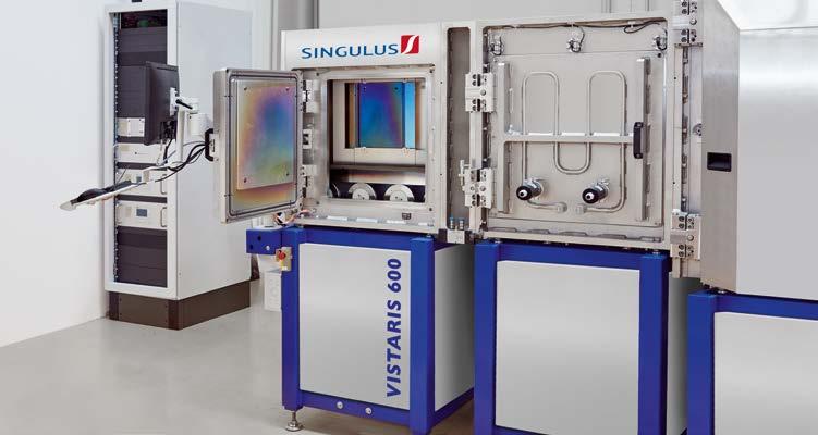
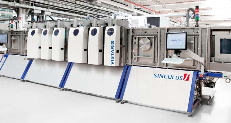
SINGULUS TECHNOLOGIES offers proven sputtering systems with vertical substrate transport with the brand name VISTARIS PVD. One major application is today’s CIGS & CdTe thin-film solar module production. These systems have been developed to enhance the efficiency of thin-film solar modules, while cutting production costs by using state-of-the-art technologies. For photovoltaic technology, SINGULUS TECHNOLOGIES develops and manufactures coating systems which apply special layers and layer stacks on different substrates. In addition to applications in the solar sector, the VISTARIS PVD offers ideal conditions for other applications such as large glass surfaces. Examples are transparent front or metallic back contact layers as well as multilayered precursors with a broad range of different materials. The VISTARIS PVD is designed for sputtering materials like ITO, AZO and metallic layers like Mo, Al, Cu, Ag, NiV, etc. The main advantage of the system is the use of vertical vacuum-based coating of glass substrates in various industries.
» For particle-free process requirements
» Carrier usage for transport of the substrates
» Tact time: up to 45 s per carrier
» Usage of rotatable cylindrical magnetrons for highest utilization of target material
» Temperature processing before and during deposition available
» DC, pDC, BP and RF process available
» Sputtering material: ITO, AZO and metallic layers like Mo, Al, Cu, Ag, NiV, etc.
» Vacuum base pressure: < 1 x 10⁻⁶ mbar
» Typical process pressure: 2 - 8 x10⁻³ mbar
» No carrier return system (CRS) required
» Temperature range for deposition: up to 200 °C
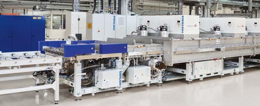
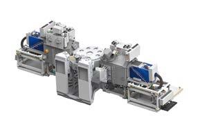
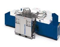
The HISTARIS PVD system was developed for the requirements in the photovoltaic industry but also for applications in large area sputtering like architectural glass, fuel cells, mobile devices, etc. The HISTARIS PVD was designed to enhance the efficiency and cutting production costs by using state-of-the-art technologies. The modular design includes process chambers equipped with rotatable magnetrons for the sputter deposition of high-performance TCO layers or several other materials, such as metals and metal oxides. Pre-treating modules for cleaning or etching can be added. With its unique modular design, the HISTARIS PVD system is ideally suited for challenging layer stacks and flexible product mixes.
Examples are transparent front or metallic back contact layers as well as multilayered precursors with a broad range of different materials. The main advantage of the HISTARIS PVD is that it can be used for horizontal vacuum-based coating of glass substrates in solar, display and many other industries. Typical applications include anti-reflection layers, barrier layers and precursor layers but also different metallic layers such as Al, Cu, NiV, etc.
The HISTARIS PVD is using an inline process in which the substrates are transported on specially designed carriers or directly on a customized roller drive system. Different automation options for loading and unloading are available.
TYPICAL PERFORMANCE CHARACTERISTICS
» Sputtering material: ITO, AZO and metallic layers like Mo, Al, Cu, Ag, NiV etc.
» Parallel processing of several substrates
» Available in three versions: HISTARIS PVD LAB / STANDARD / SPEED
» Modular configuration
» Low cost of ownership and high uptime
» Top down and bottom-up sputtering configurable
» Sputter sequence configurable
» DC, pDC, BP and RF process available
» Rotatable cylindrical magnetrons for highest utilization of target material
» Single end and double end version selectable
» Manual or semi-automated lab versions
» Tact time: up to 20 s per batch (without carrier)
» Highest deposition rates
» Temperature processing during deposition available
» Gas separation by dynamic slit valves and/or by individual lock chambers
» Vacuum base pressure: ‹ 1 x 10⁻⁶ mbar, typical process pressure: 2 - 5 x10⁻³ mbar
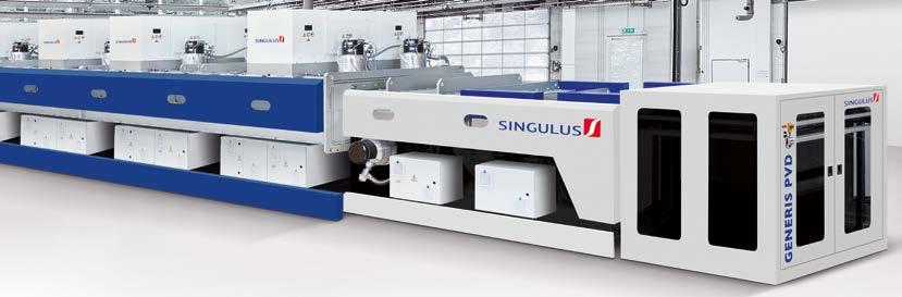
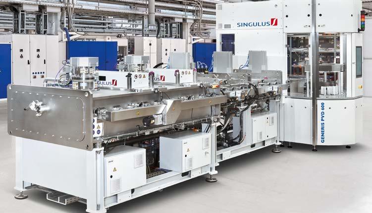
Numerous SINGULUS TECHNOLOGIES vacuum sputtering machines are in operation in the solar industry, where SINGULUS TECHNOLOGIES provides the GENERIS PVD as a high throughput inline sputtering system platform with horizontal substrate transport. The GENERIS PVD ideally meets the key requirements of the heterojunction solar cell technology with respect to sophisticated transparent conductive oxide layers (TCO) such as ITO (Indium Tin Oxide) and AZO (Aluminum doped Zinc Oxide). The solar cells are automatically transported through the process chambers of the GENERIS PVD, following the inline principle, and applying coatings on both sides. The sputtering system safeguards a high level of layer thickness uniformity with high layer reproducibility, high productivity and at the same time very low operating expenses (OPEX).
With the latest system generation GENERIS PVD, SINGULUS TECHNOLOGIES can assure capacities up to 8,000 wafers per hour of G12 HJT cells. There are further savings due to the smaller footprint of the equipment and related smaller building and cleanroom space requirements. The dual-sided processes of the GENERIS PVD require less wafer handling resulting in reduced wafer breakage, wafer damage and wafer marks. SINGULUS TECHNOLOGIES takes advantage of in-house engineering of crucial components such as sputtering magnetrons, simulation and optimization of different sputtering processes
and processes developed using state-of-theart sputtering lab equipment at SINGULUS TECHNOLOGIES R&D center. Newly developed processes can be directly industrialized to the GENERIS PVD mass production platform.
TYPICAL PERFORMANCE CHARACTERISTICS
» Sputtering materials: TCOs and other reactively sputtered layers: ITO, AZO, NiO, TiO2, SiN and more metallic layers: Ag, Cu, Cr, Mo, Ni and more
» Applications include anti-reflection layers, barrier layers, electrical contacting or insulating layers
» Available in different throughput versions of lab, pilot & mass production
» Wafer size: up to G12 & half cut formats
» Substrates thickness down to 60 µm
» Typical tact time: 40 - 75 s per carrier
» Parallel processing of substrates (e.g. display, glass, Si wafers) via carrier tray
» High-speed automatization for carrier tray loading and unloading (single or double side)
» Top-down and bottom-up sputtering configurable – dual side sputtering without vacuum breakage
» Full substrate temperature control
» Low cost of ownership and high uptime
» Patented features such as fast venting systems and carrier
» Rotatable cylindrical magnetrons with highest utilization of target material
» Carrier return system (CRS) underneath
» Vacuum base pressure: ‹ 1 x 10⁻⁶ mbar
Whether in cosmetic, white goods or automotive –metallic quality surfaces are needed more than ever in the decorative sector. However, the coating (sputtering) of sensitive layers is usually an expensive step. A fully automated inline sputtering system with the brand name POLYCOATER is being successfully introduced to resign products and parts for different applications.
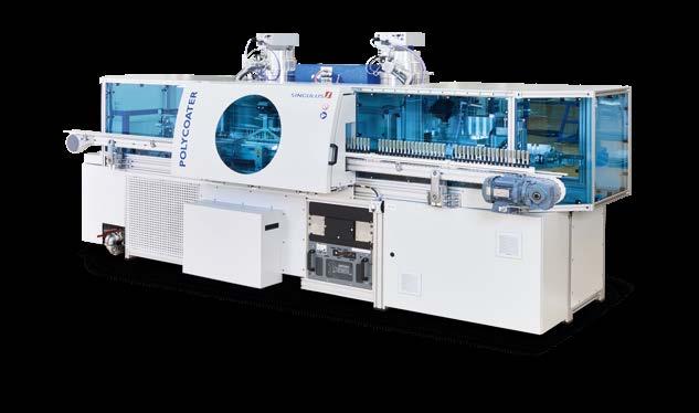
SINGULUS TECHNOLOGIES offers with the POLYCOATER the second generation of inline coating solutions for fully automated handling and coating of 3-dimensional parts. From loading to packaging, the process is fully automated at a cycle time of down to 6 seconds per carrier. This manufacturing solution is interesting for automotive, consumer goods, mobile phones and packaging for the cosmetics or beverage industry.
The sputtering module can be interlinked with different innovative handling concepts, which provide the possibility of incorporation of additional production modules (e.g. pretreatment, lacquering module, robot handling systems). The POLYCOATER can be integrated into the existing production flow. An exchange handling system is loading new parts and is unloading the metallized parts to an interface position. The POLYCOATER is the result of the combination of proven coating technologies, high performance expertise and unique experience bundled with a revolutionary concept for the application of 3-dimensional coating onto parts. Not only decorative, but also functional layers can be applied. Possible approaches are antibacterial coatings, EMV-shielding, electrically conductive layers (e.g. on electroplating components before the process) or antennas. Each electrically conductive and nonmagnetic metal and its alloys
can be used as a metallic layer. This is a clear unique selling point, compared to batch processes, in which the selection of possible coating materials is much more limited. The POLYCOATER offers a reproducible layer uniformity and high deposition rates with highest coating quality and a high uptime resulting from a permanent sputtering process control.
» Inline or standalone metallizer system
» Cycle time per carrier: down to 6 s
» Up to 18 substrates per carrier
» Substrate rotation during sputtering process
» Equipped with two cathodes (1x top, 1x side)
» Substrate diameter 68 mm or 90 mm
» Reactive sputtering process possible
» Target materials e.g.: Al, Cu, Stainless Steel, Cr, Zr, CuAl, Ag, Au, SiOx, TiOx, (all electrically conductive metals, non-magnetic)
POLYCOATER 68
» Production cycle time: down to 6 s per carrier
» 1 substrate per carrier: 480 x 130 x 68 mm
» 6 substrates per carrier: Ø 68 x 130 mm
» 9 substrates per carrier: Ø 45 x 130 mm
» 18 substrates per carrier: Ø 22 x 130 mm
» Substrate diameter: 68 mm
» Substrate height max.: 130 mm
POLYCOATER 90
» Production cycle time: down to 10 s per carrier
» 1 substrate per carrier: 480 x 130 x 90 mm
» 4 substrates per carrier: Ø 90 x 130 mm
» 6 substrates per carrier: Ø 68 x 130 mm
» 9 substrates per carrier: Ø 45 x 130 mm
» 18 substrates per carrier: Ø 22 x 130 mm
» Substrate diameter: 90 mm
» Substrate height max.: 130 mm
SINGULUS TECHNOLOGIES IS MARKET AND TECHNOLOGY LEADER FOR MAGNETIC STRUCTURES AND SPINTRONIC, E.G.:
» MRAM
» Thin-film heads
» Magnetic sensors
» Integrated inductors
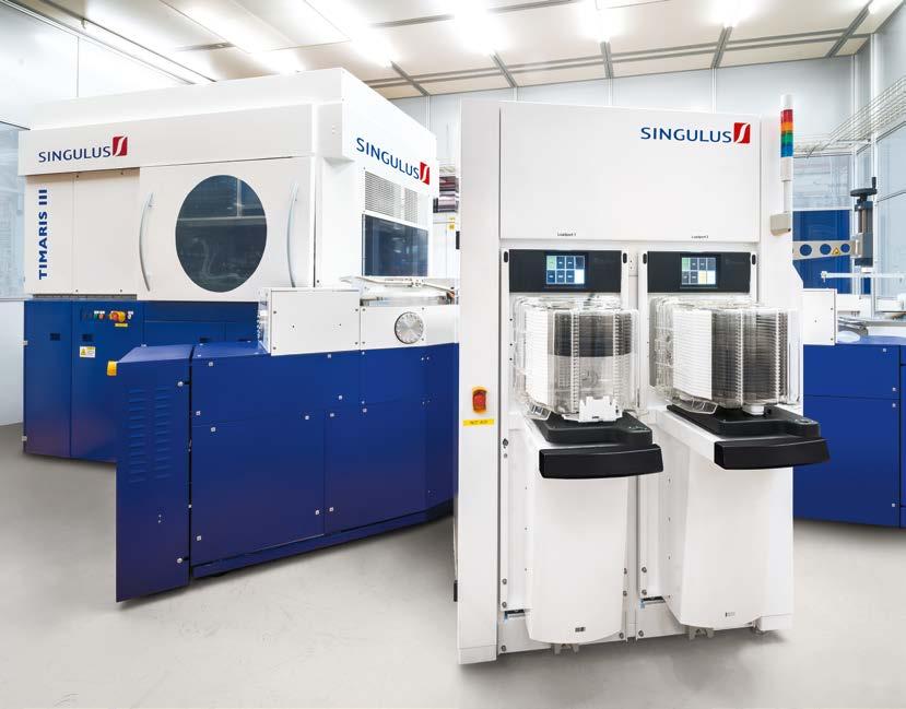
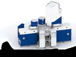
THE TIMARIS CLUSTER TOOL IS PERFECTLY FITTING TO A WIDE RANGE OF APPLICATIONS FOR EXAMPLE:
» Advanced packaging
» µLED
» Power electronics
» MEMS
» RF-filter
VERSATILE
Thanks to the broad spectrum of available deposition and conditioning modules the TIMARIS Cluster Tool is the ideal PVD production platform for a wide range of applications in the semiconductor industry.
FUTURE-PROOF
It fulfills all connectivity standards of modern 200 mm and 300 mm foundries and is compatible with GEM300 and SECS/GEM host interfaces and allows advanced process control (APC) necessary for state-of-the art quality control. All modules are capable to handle 200 mm and 300 mm wafers (smaller wafers via adapters).
COST EFFICIENT
SINGULUS TECHNOLOGIES offers modules with several targets and integrated heating/cooling/ aligning magnetic field (AMF). This allows to very efficiently manufacture complex multi-layerstructures in just one module, saving cleanroom space as well as production time through reduction of unnecessary inter-module transfers.
PRECISE
Thanks to the patented Linear-DynamicDeposition-Technology (LDD) the TIMARIS Cluster Tool is perfect the deposition film with ultraprecise thickness control down to 0,01 nm and high uniformity. However, this technology can also be used for applications with thicknesses in the micrometer range. The high target utilization allows long lifetime before a target change.
As of today, more than ten process modules are available to configure a TIMARIS system according to customer needs. These modules include the MultiTarget-Module, Oxidation-Process-Module, PreClean-Module, Combi-Process-Module, Four-TargetModule and Static-Deposition-Module as well as the Rotating-Substrate-Module. The RotatingSubstrate-Module is extremely versatile with up to twelve cathodes, possibility to co-sputter, DC and RF. The TIMARIS PVD modules incorporate the full scope of sputtering techniques as: DC magnetron sputtering, pulsed DC magnetron sputtering and RF magnetron sputtering as well as combinations of these modes are selectable by recipe.
The TIMARIS Cluster Tool is dedicated for the deposition of ultra-thin metallic and insulating films down to a thickness of one nanometer and below and stacks of such films with very precise material thickness and high uniformity specifications. SINGULUS TECHNOLOGIES has already established and qualified the second and third generation of the TIMARIS PVD Cluster Tool platform in the market and is offering a complete portfolio of process modules for different applications. As of today, more than ten process modules are available to configure a TIMARIS system according to customer needs. These modules include the Multi-Target-Module, Oxidation-ProcessModule, Pre-Clean-Module, Combi-Process-Module, Four-Target-Module and Static-Deposition-Module as well as the Rotating-Substrate-Module. The TIMARIS PVD modules incorporate the full scope of sputtering techniques as: DC magnetron sputtering, pulsed DC magnetron sputtering and RF magnetron sputtering as well as combinations of these modes are selectable by recipe.
» Up to 10 targets in one deposition chamber
» High throughput for multilayer deposition with short change time between the materials
» Outstanding homogeneity due to the patented Linear Dynamic Deposition (Patent US 7,799,179)
» Excellent sub-Å thickness control with high repeatability
» Very long target life with optimized coating efficiency
» Low cost of ownership
» Qualified processes for production
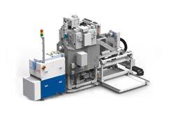
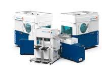
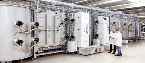
GENERIS PVD 600 – PVD sputtering system with automatic substrate loading, e.g. for mobile applications
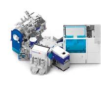
VISTARIS PVD 600 – PVD sputtering system for R&D with vertical cathode arrangement
SINGULUS TECHNOLOGIES develops technologies for economic and resource-efficient production processes. The applications include vacuum sputtering, surface engineering as well as thermal process technologies.
SINGULUS TECHNOLOGIES continues to emphasize on the new and further development of PVD production equipment for new applications. The core competence of SINGULUS TECHNOLOGIES is the development of new vacuum deposition systems for use in mass production, pilot production and laboratory applications. The implementation of individual customer requirements is tested in R&D as well as in pilot production and the results are transferred to inline mass production.
For example, single substrates deposition machines are used for R&D and testing of new applications, display and touch screen devices with applications like ITO coatings, AR coatings, EMI shielding and coatings for so called one glass solution technology. The transfer from R&D to inline sputtering machines secures the use of layers systems of high conductivity and transparency and various other metal coatings at the same time.
Your direct contact: www.singulus.com
Headquarters
SINGULUS TECHNOLOGIES AG
Hanauer Landstrasse 103
63796 Kahl, Germany
Tel. +49 6188 440-0
Fax +49 6188 440-1130 sales@singulus.de
Subsidiaries
China
SINGULUS TECHNOLOGIES
(SHANGHAI) Co. Ltd.
Room B412-413
No. 1400 Jiangchang Road
Jingan District, Shanghai Zip Code: 200072
Tel. +86 21 61073997 sales@singulus.cn
SINGULUS TECHNOLOGIES
Guangzhou Office
Room 539, 5F Block B Nanlong Commercial Center
Dalong No.31 Shilian Road, Panyu
Guangzhou 511450
Tel. +86 13822138376 sales@singulus.cn
France
SINGULUS TECHNOLOGIES
FRANCE S.A.R.L.
Tel. +33 3 8931 1129 laurent.ferrer@singulus.fr
North America
SINGULUS TECHNOLOGIES INC.
Tel. +1 860 683 8000 sales@singulus.com
South America
SINGULUS TECHNOLOGIES
LATIN AMERICA LTDA. Tel. +55 1121 6524-10 sales@singulus.com.br
Southeast Asia
SINGULUS TECHNOLOGIES
ASIA PACIFIC PTE LTD.
Tel. +65 67411912 sales@singulus.com.sg
Taipei Office
SINGULUS TECHNOLOGIES
TAIWAN LTD.
Tel. +886 2 8692 6996 sales@singulus.com.tw
SINGULUS TECHNOLOGIES develops and assembles innovative machines and systems for efficient thin-film coating and surface treatment processes, which are used worldwide in the Photovoltaics, Semiconductor, Medical Technology, Packaging, Glass & Automotive as well as Battery & Hydrogen markets. The company’s core competencies include various processes of coating technology, surface treatment as well as wet-chemical and thermal production processes. SINGULUS TECHNOLOGIES sees sustainability as an opportunity to position itself with innovative products. In the focus are:
» Environmental awareness
» Efficient use of resources
» Avoidance of unnecessary CO₂ pollution
SINGULUS TECHNOLOGIES attaches great importance to responsible and sustainable corporate governance.