TYPICAL PERFORMANCE CHARACTERISTICS
» Sputtering materials: TCOs and other reactively sputtered layers: ITO, AZO, NiO, TiO2, SiN and more metallic layers: Ag, Cu, Cr, Mo, Ni and more
» Applications include anti-reflection layers, barrier layers, electrical contacting or insulating layers
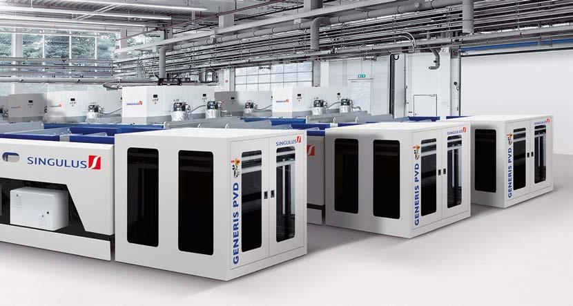
» Available in different throughput versions of lab, pilot & mass production
» Wafer size: up to G12 & half cut formats
» Substrates thickness of down to 60 µm
» Typical tact time: 40 - 75 s per carrier
» Parallel processing of substrates, e.g. display, glass, Si wafers, via carrier tray
» High-speed automatization for carrier tray loading and unloading (single or double side)
» Top-down and bottom-up sputtering configurable – dual side sputtering without vacuum breakage
» Full substrate temperature control
» Low cost of ownership and high uptime
» Patented features such as fast venting systems and carrier
» Rotatable cylindrical magnetrons with highest utilization of target material
» Carrier return system (CRS) underneath
» Vacuum base pressure: ‹ 1 x 10⁻⁶ mbar

Your direct contact: www.singulus.com
Headquarters
SINGULUS TECHNOLOGIES AG
Hanauer Landstrasse 103
Kahl, Germany
6188 440-1130 sales@singulus.de
Subsidiaries
China SINGULUS TECHNOLOGIES
(SHANGHAI) Co. Ltd.
Room B412-413
No. 1400 Jiangchang Road
Jingan District, Shanghai Zip Code: 200072
Tel. +86 21 61073997 sales@singulus.cn
SINGULUS TECHNOLOGIES
Guangzhou Office
Guangzhou Office Room 539, 5F Block B
Nanlong Commercial Center
Dalong No.31 Shilian Road, Panyu Guangzhou 511450
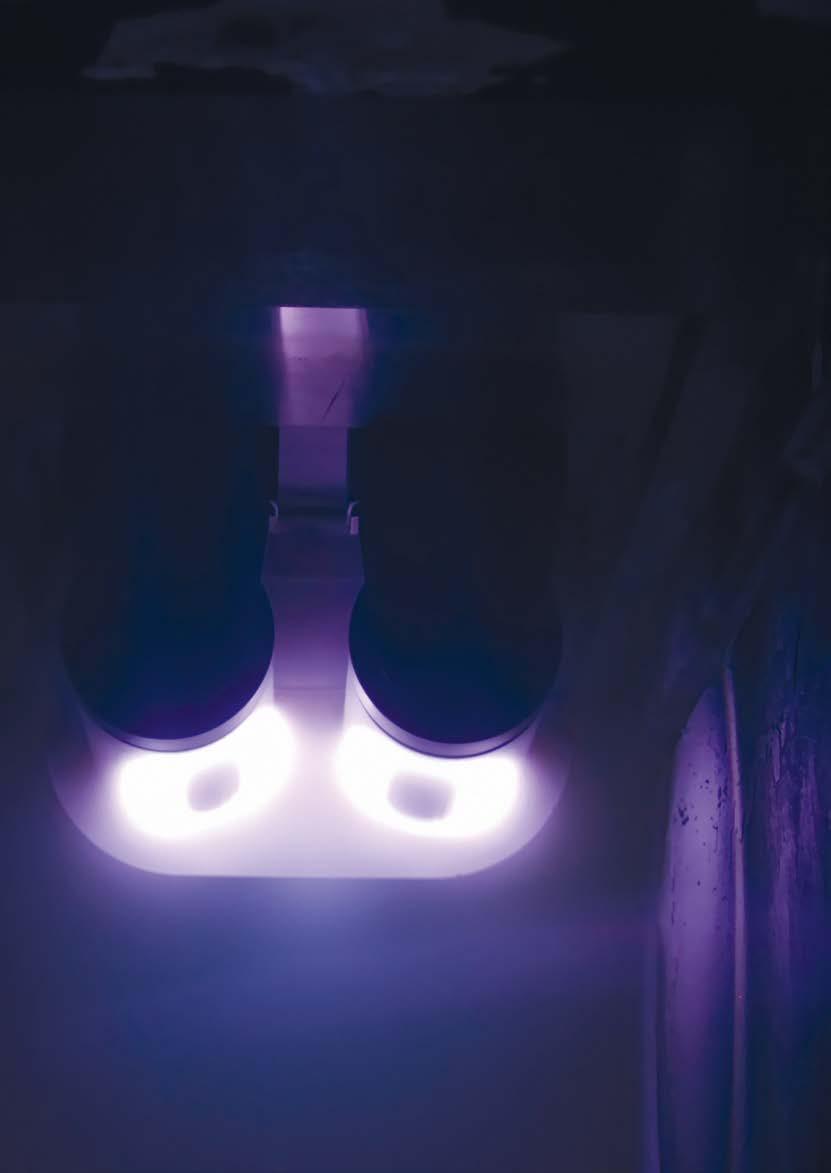
ROTARY MAGNETRONS WITH INTENSIVE COOLING AND HIGHEST MATERIAL/TARGET UTILIZATION
» Target utilization about 80 % for rotatable cathodes compared with only 30 % for planar cathodes
» Stable processes with ceramic targets
» Long-life rotary seals
» Maintenance on customers’ site
» Advanced water fill and drain features
» Flexible target attachment method and non-proprietary target design
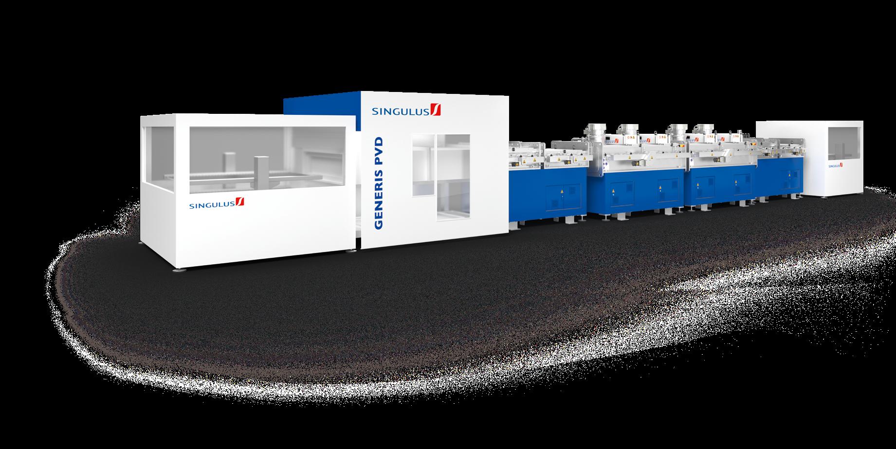
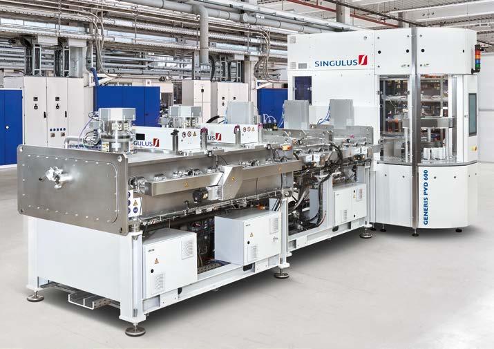
GENERIS PVD
Technical Data
Application Heterojunction solar cells & other high-performance products
Substrate size Up to G12 & half cut formats
Cycle time 40 - 75 s per carrier, depending on configuration
Carrier size 80 wafers (M6) per carrier
Sputtering materials TCOs and other reactivly sputtered layers: ITO, AZO, NiO, TiO2 and metallic layers: Ag, Cu, Cr, Mo, Ni and more
Sputter orientation Top down/bottom up
Vacuum base pressure 1 x 10⁻⁶ mbar
Variable configurations Pretreatment solutions, gas separations, top-down and bottom-up deposition, multiple heating concepts
Tel. +86 13822138376 sales@singulus.cn
France SINGULUS TECHNOLOGIES
FRANCE S.A.R.L.
Tel. +33 3 8931 1129 laurent.ferrer@singulus.fr
South America
SINGULUS TECHNOLOGIES
LATIN AMERICA LTDA.
Tel. +55 1121 6524-10 sales@singulus.com.br
Southeast Asia
SINGULUS TECHNOLOGIES
ASIA PACIFIC PTE LTD.
Tel. +65 67411912 sales@singulus.com.sg
Taipei Office
SINGULUS TECHNOLOGIES
TAIWAN LTD.
Tel. +886 2 8692 6996 sales@singulus.com.tw
North America
SINGULUS TECHNOLOGIES INC.
Tel. +1 860 683 8000 sales@singulus.com
SINGULUS TECHNOLOGIES - Thin-Film Coating and Surface Treatment
SINGULUS TECHNOLOGIES develops and assembles innovative machines and systems for efficient thin-film coating and surface treatment processes, which are used worldwide in the Photovoltaics, Semiconductor, Medical Technology, Packaging, Glass & Automotive as well as Battery & Hydrogen markets.
The company’s core competencies include various processes of coating technology, surface treatment as well as wet-chemical and thermal production processes.
SINGULUS TECHNOLOGIES sees sustainability as an opportunity to position itself with innovative products. In the focus are:
» Environmental awareness
» Efficient use of resources
» Avoidance of unnecessary CO₂ pollution
SINGULUS TECHNOLOGIES attaches great importance to responsible and sustainable corporate governance.