
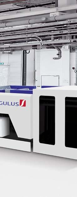
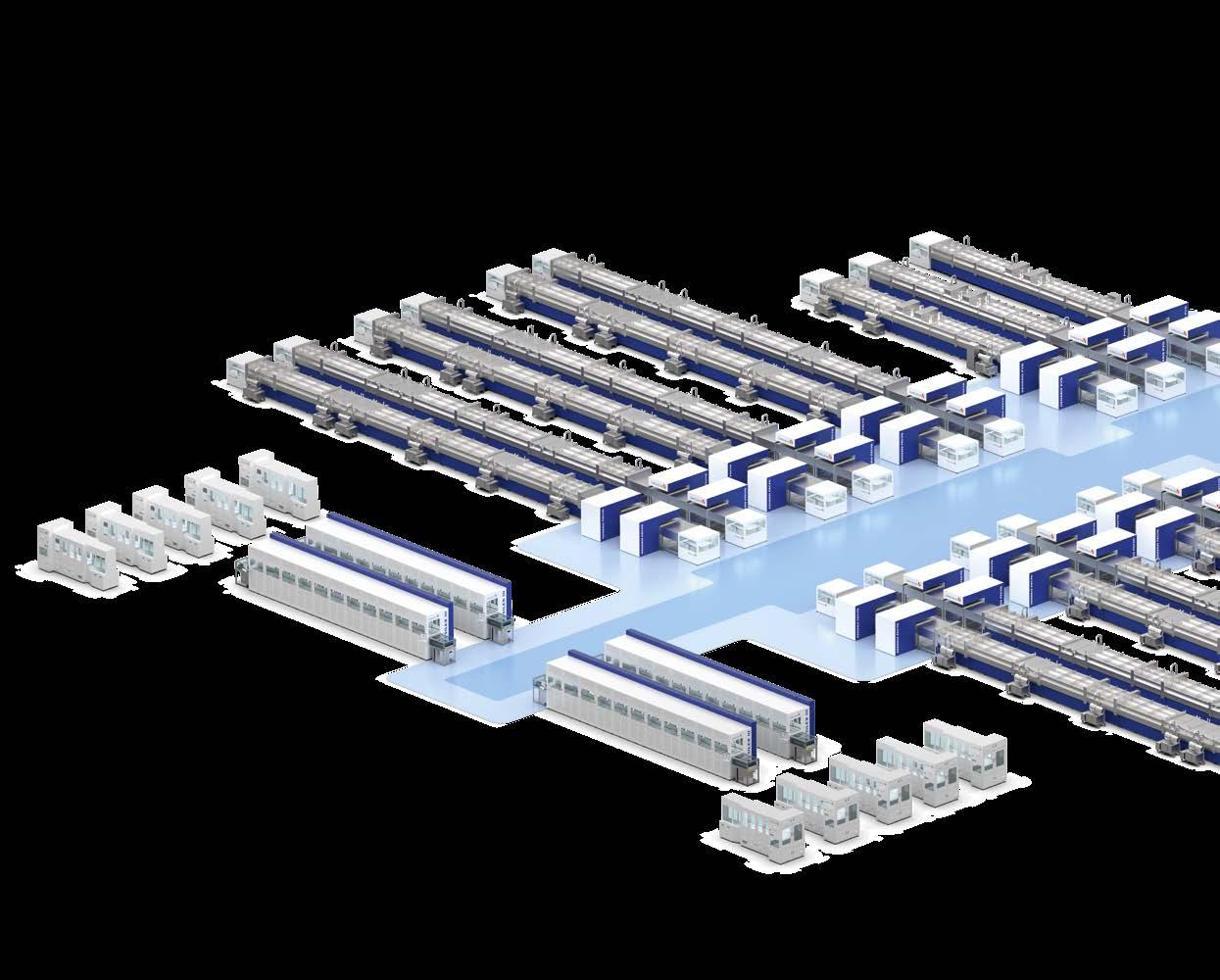
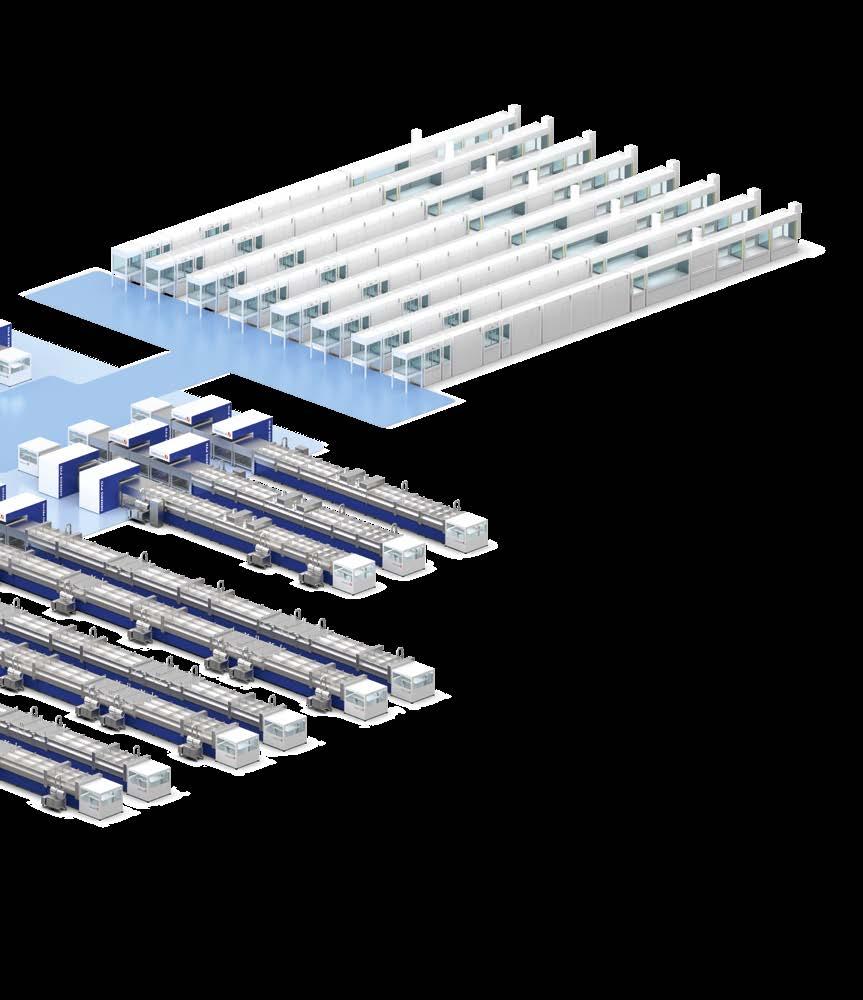
EQUIPMENT FOR GW CELL PRODUCTION
...for HJT, Perovskite and more
...for HJT, Perovskite and more
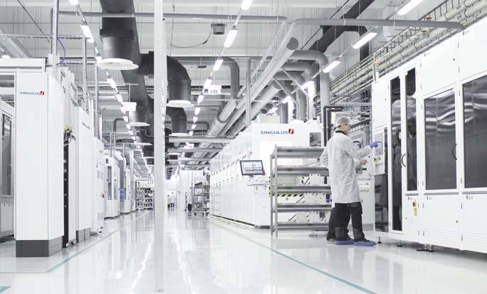
SINGULUS TECHNOLOGIES develops innovative systems and technologies for efficient and resource-friendly production processes, taking advantage of its existing core technologies including vacuum thin-film coating, surface engineering, wet-chemical and thermal processes as well as automation and process control. The company offers machines worldwide in the market sectors Photovoltaics, Semiconductor, Medical Technology, Packaging, Glass & Automotive as well as Battery & Hydrogen.
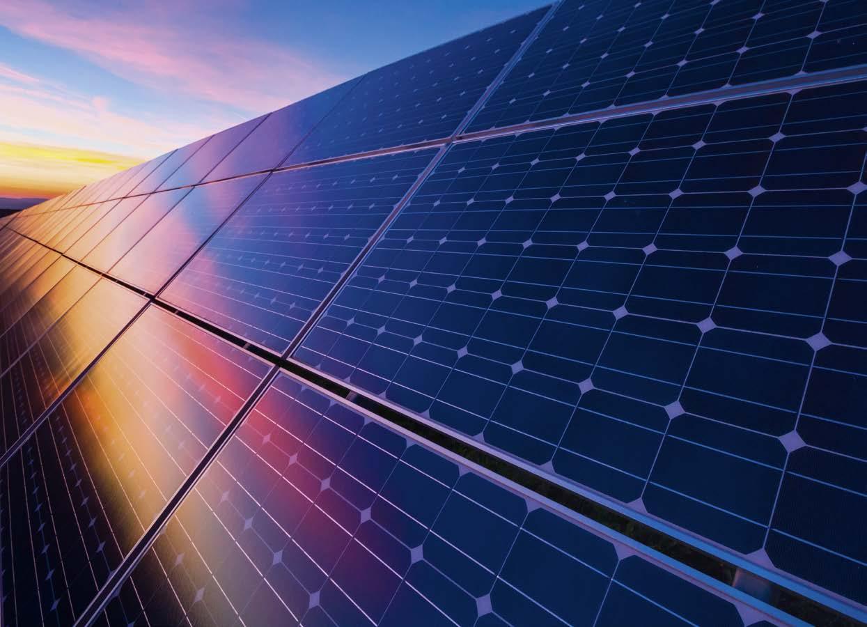
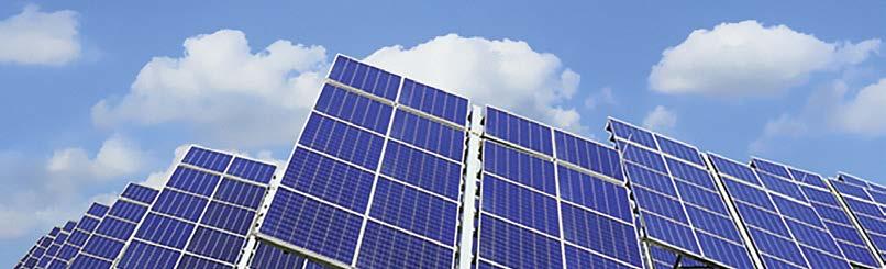
A carbon neutral energy system is one of the biggest challenges in the world. Solar power is at the forefront of being one important pillar for sustainable energy supply. Highly efficient photovoltaic cells will pave the road to this destination. Modern storage and battery technologies will sharply increase the use of environmentally friendly energy.
SINGULUS TECHNOLOGIES production equipment follows the requirements of the latest PV cell processes, high throughput, low material and media consumption, thus enabling to improve cell efficiency, to save energy and raw materials and to reduce manufacturing costs for highly efficient solar cells.
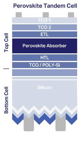
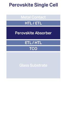
New cell concepts such as perovskite-silicon and perovskite tandem cells combine complementary absorber materials to capture a broader spectrum of sunlight. This enables record efficiencies well above conventional silicon limits, with current laboratory results exceeding 30 % for perovskitesilicon tandems and promising further gains. The technology offers significant potential for reducing the levelized cost of electricity (LCOE) through higher power output per module and improved performance under low-light conditions.
The transfer of this new, highly efficient solar cell concepts into industrial mass production, requires reliable machines covering the following process steps:
Perovskite and Tandem PV
» PVD sputtering
» Evaporation
» PECVD (Plasma Enhanced Chemical Vapour Deposition)
» PET passivation
» Wet-chemical processes
» Specific thermal processes to achieve optimum layer properties
» Turn-key production lines
» A combination of vacuum, wet-chemical, and thermal process technologies for the fabrication of tandem solar cells
New Functions Processes
TCO
Buffer layer
ETL
Absorber
HTL
Interface layers between silicon and perovskite cell
Optimized surface structure of silicon bottom cell
Soft sputtering
Probably avoidable (soft sputtered TCO)
Evaporation
Evaporation or hybrid process
Sputtering (evaporation)
Hybrid sputtering and self assembled monolayer
Wet-chemical processes, batch or inline
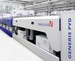
Numerous SINGULUS TECHNOLOGIES vacuum sputtering machines are in operation in the solar industry, where SINGULUS TECHNOLOGIES provides the GENERIS PVD as a high throughput inline sputtering system platform with horizontal substrate transport. The GENERIS PVD ideally meets the key requirements of the heterojunction solar cell technology with respect to sophisticated transparent conductive oxide layers (TCO) such as ITO (Indium Tin Oxide) and AZO (Aluminum doped Zinc Oxide). The solar cells are automatically transported through the process chambers of the GENERIS PVD, following the inline principle, and applying coatings on both sides. The sputtering system safeguards a high level of layer thickness uniformity with high layer reproducibility, high productivity and at the same time very low operating expenses (OPEX).
With the latest system generation GENERIS PVD, SINGULUS TECHNOLOGIES can assure capacities up to 8,000 wafers per hour of G12 HJT cells. There are further savings due to the smaller footprint of the equipment and related smaller building and cleanroom space requirements. The dual-sided processes of the GENERIS PVD
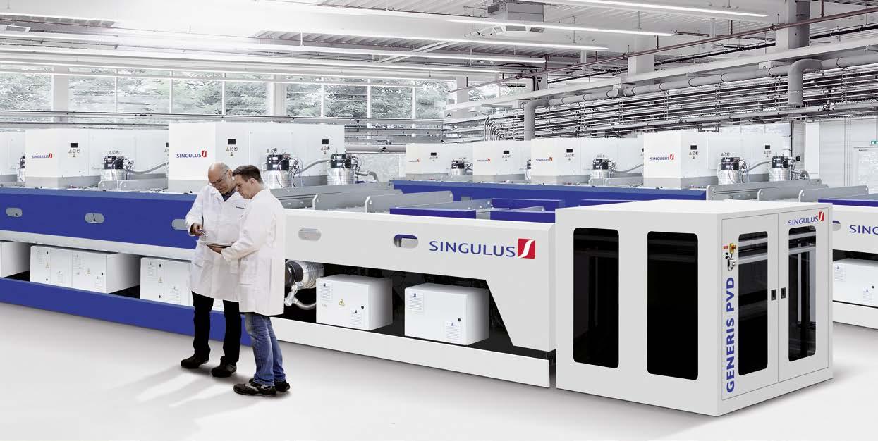
require less wafer handling resulting in reduced wafer breakage, wafer damage and wafer marks. SINGULUS TECHNOLOGIES takes advantage of in-house engineering of crucial components such as sputtering magnetrons, simulation and optimization of different sputtering processes and processes developed using stateof-the-art sputtering lab equipment at SINGULUS TECHNOLOGIES R&D center. Newly developed processes can be directly industrialized to the GENERIS PVD mass production platform.
TYPICAL PERFORMANCE CHARACTERISTICS
» Sputtering materials: TCOs and other reactively sputtered layers: ITO, AZO, NiO, TiO2, SiN and more metallic layers: Ag, Cu, Cr, Mo, Ni and more
» Applications include anti-reflection layers, barrier layers, electrical contacting or insulating layers
» Available in different throughput versions of lab, pilot & mass production
» Wafer size: up to G12 & half cut formats
» Substrates thickness of down to 60 µm
» Typical tact time: 40 - 75 s per carrier
» Parallel processing of substrates (e.g. display, glass, Si wafers) via carrier tray
» High-speed automatization for carrier tray loading and unloading (single or double side)
» Top-down and bottom-up sputtering configurable – dual side sputtering without vacuum breakage
» Full substrate temperature control
» Low cost of ownership and high uptime
» Patented features such as fast venting systems and carrier
» Rotatable cylindrical magnetrons with highest utilization of target material
» Carrier return system (CRS) underneath
» Vacuum base pressure: ‹ 1 x 10⁻⁶ mbar
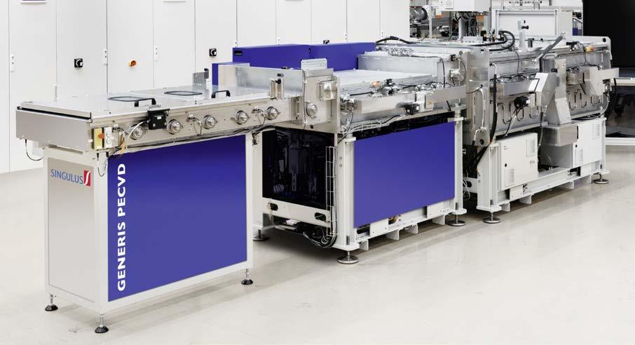
SINGULUS TECHNOLOGIES employs inductively coupled plasma (ICP) and capacitively coupled (CCP) sources for inline PECVD coating applications. ICP is a method that offers a high electron and activation density in conjunction with low ion energy, which allows very high deposition rates over a large width and extraordinary layer quality with wide process windows at low substrate damage. Therefore, ICP plasma sources are ideally suitable for high-rate and low-damage mass production of electronic devices like solar cells. CCP is an ideal method for depositing of thin or thick conductive layers, highly doped as needed in the PV cell technology.
SINGULUS TECHNOLOGIES has developed new, large-scale linear plasma sources based on ICP and CCP technology. Both technologies are used for processes developed using state-ofthe-art PECVD lab equipment at SINGULUS TECHNOLOGIES R&D center.
SINGULUS TECHNOLOGIES has also delivered systems for the deposition of functional layers for the production of gallium arsenide (GaAs) photovoltaic cells. The PECVD coating step is a crucial quality factor for GaAs solar cells that are renowned to achieve very high efficiency in excess of 35 % in multi-junction setup and that are used in space applications for the power generation of satellites.
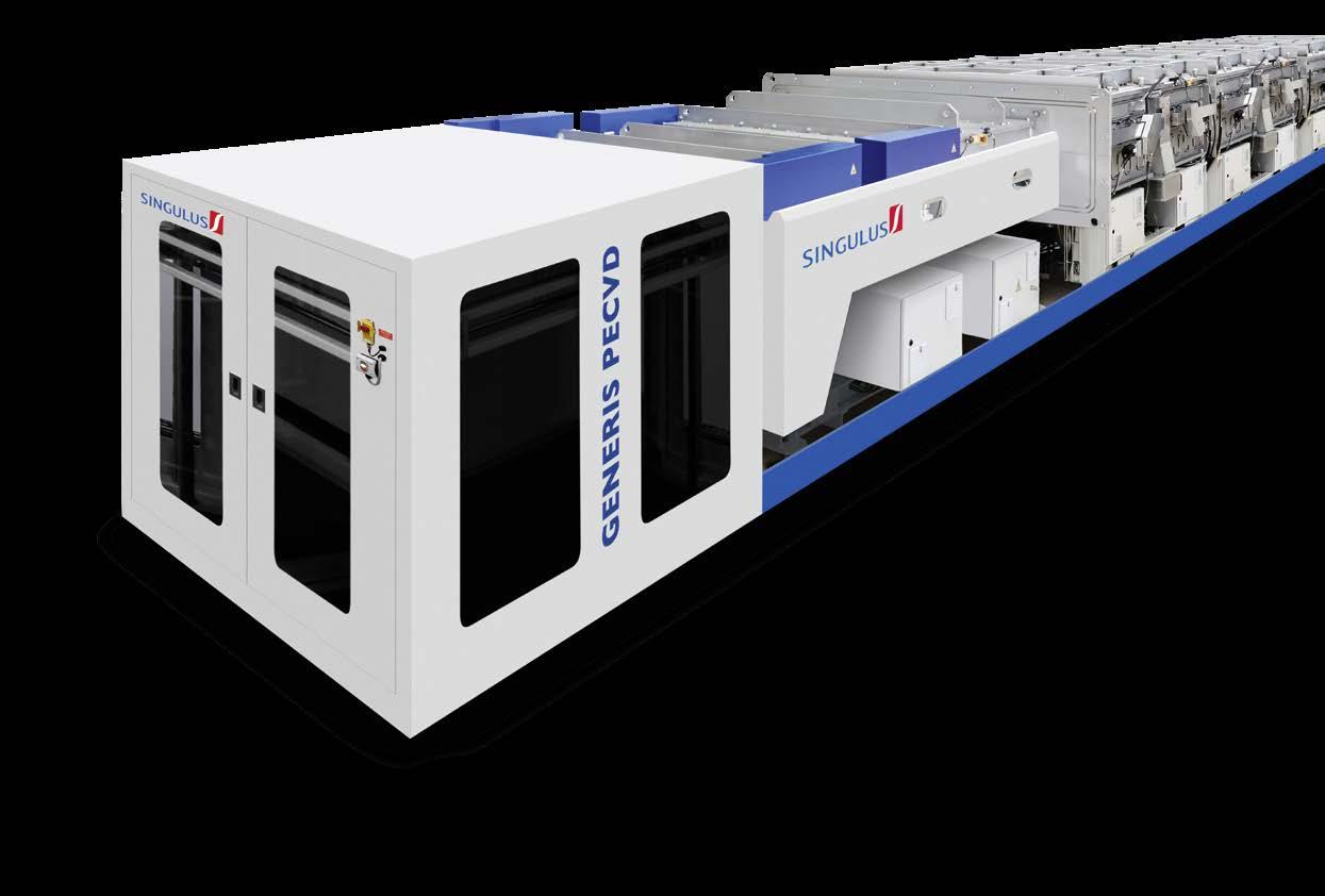
The GENERIS PECVD is a modular horizontal inline tool designed for the special needs in mass production of state-of-the-art crystalline silicon solar cells with highest efficiencies, such as passivated emitter and rear cells (PERC) and cells with passivated contacts (e.g., TOPCon, POLO and HJT). PERC solar cells are coated on both sides with dielectric passivation layers. Rear side passivation is achieved by deposition of a thin
aluminum oxide (AlOx) layer capped by hydrogen rich silicon nitride (SiNx:H). On the front side, a layer of SiNx:H serves as both, passivation, and anti-reflective coating (ARC).
Cells with passivated contacts are coated with conducting amorphous a-Si:H(n,p) or polycrystalline silicon poly-Si:H(n,p) layers single sided in the case of TOPCon or POLO cell structures or both sides in the case of HJT technology. The modular systems are ideally suited for cost effective mass production with high throughput, high uptime, short cleaning interruptions and maximum utilization of raw materials. The substrate temperature is fully controlled during the whole process, which enables optimum layer performance at temperatures from 200 °C to 500 °C for HJT, PERC and TOPCon cells. The thermal properties can be adapted in a wide range for other layer stacks and applications. SINGULUS TECHNOLOGIES carriers allow single side deposition with close to zero wrap-around.
The GENERIS PECVD allows for deposition on both sides of the wafer without vacuum interruption. The application of both processes AlOx and SiNx are realized in one common system with a gas separation chamber. Same gas separation chamber enables the deposition of intrinsic and doped amorphous layers without vacuum breakage.
Especially the configuration in which all PECVD layers are deposited in one tool represents a cost attractive, highly productive, and straight forward production solution. High-rate inline deposition of these dielectric or conductive semiconductor structures without wrap-around allows future industrial mass production of more advanced and ultra-high efficient cell architectures like TOPCon, XBC and tandem (e.g. plus Perovskite) solar cells.
TYPICAL PERFORMANCE CHARACTERISTICS
» PECVD materials: a-Si(i,n,p) nc-Si(i,n,p) poly-Si(i,n,p) AlOx, SiNx SiOx and more
» Typical applications include anti-reflection layers, barrier layers, electrical contacting or insulating layers
» Available in different versions up to 5,800 wph for G12
» Wafer size: up to G12 & half cut formats
» Typical cycle time: 35 - 70 s per carrier
» Parallel processing of substrates (e.g., display, glass, Si wafers) via carrier tray
» High-speed automatization for carrier tray loading and unloading (single or double side)
» Top-down and bottom-up deposition configurable –dual side deposition without vacuum breakage
» Full substrate temperature control
» Low cost of ownership and high uptime
» Coating sequence configurable
» Highest utilization of precursor material
» Carrier return system (CRS) underneath of machine
Solar modules comprising cut cells are meanwhile part of the standard portfolio of almost every solar module manufacturer and supplier, with an increasing trend towards half cut/multi cut cells and shingle technology. The shingle technology uses solar cells not only being cut in half but also into multiple strips (3, 4 to 8). By dividing the cells, the electrical resistance of the metallization decreases, leading to a higher efficiency of the solar modules in comparison to the use of full cells, e.g., M10, G12. This even overcompensates Voc losses caused by damaged edges after cutting processes.
However, each cut facilitates charge recombination processes occuring on the newly created unpassivated cut edges that ultimately lead to efficiency losses on cell level. In this regard, a further significant boost in module performance can be achieved by the Passivated Edge Technology (PET). This technology involves the deposition of a passivation layer on the cut edges which serves to recover the losses derived from cutting, enhances the overall performance of the cut cell and finally increases the efficiency gain of the module even further.
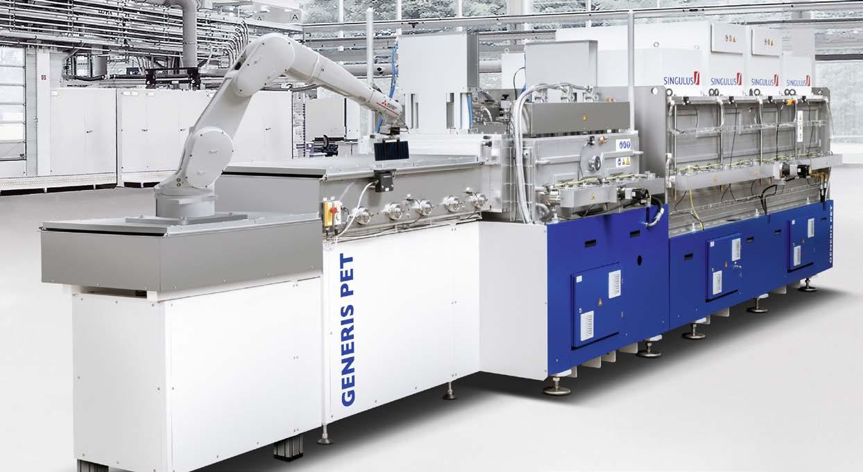
SINGULUS TECHNOLOGIES offers the new vacuum deposition system GENERIS PET, an industrialized solution for PET that is particularly characterized by high throughputs at low cost.
Standard (Full) Cell
Passivated Cut Edges
CELL CUT AFTER FINISHED CELL FABRICATION
» Less automatization/wafer handling during cell processing
» Lowering breakage rate (only full wafer handling)
Half Cut Cell
Unpassivated Cut Edges
Unpassivated wafer edges lead to efficiency loss after cutting
After cell cutting, typically performed by a laserbased process, the half cells or cell stripes are bundled into stacks. The stack transfer and loading on the carrier tray of GENERIS PET is fully automated. A unique, in-house developed carrier tray design facilitates processing of several thousand cell parts (stripes) per tray due to the high packing density. In addition, it enables the deposition of the passivation layers to be restricted to the cut edges, thus preventing undesired wraparound of the passivation to the cell surfaces.
The GENERIS PET represents an industrialized inline solution for PET that can achieve half-cell throughputs of several GW per year, depending on the equipment configuration and is readily suitable for any crystalline solar cell technology. The universal GENERIS PET design allows for processing of all current and future wafer and cut formats. In addition, its stand-alone design features facile integration into existing solar cell and module manufacturing lines and fabs as well as utilization as a stand-alone tool along with the laser cutting tool.
SINGULUS TECHNOLOGIES offers different versions of the GENERIS PET for the passivation of exposed cut edges of half cut/multi cut solar cells and shingle cells resulting from the cutting process.
The GENERIS PET represents a superior, industrialized solution for PET, characterized by:
» Processability of all types of wafer and cut formats (Half Cut/Multi Cut and Shingle Cells)
» High throughput
» Excellent passivation layer properties to improve efficiency on cell/module level
» Adaptable carrier and tray design
» Enabling cell cutting after finished cell fabrication
» Retrofittable to existing fabs due to its stand-alone machine design
» Very low payback time (ROI)
» High recovery of efficiency losses induced by cell cutting
In summary, the excellent passivation layer properties achieved by the GENERIS PET serve towards regaining up to 80% of the efficiency losses created on cell level by the cutting process compared to its unpassivated counterpart.
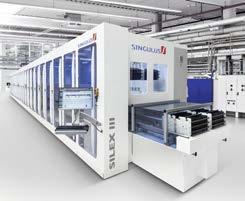
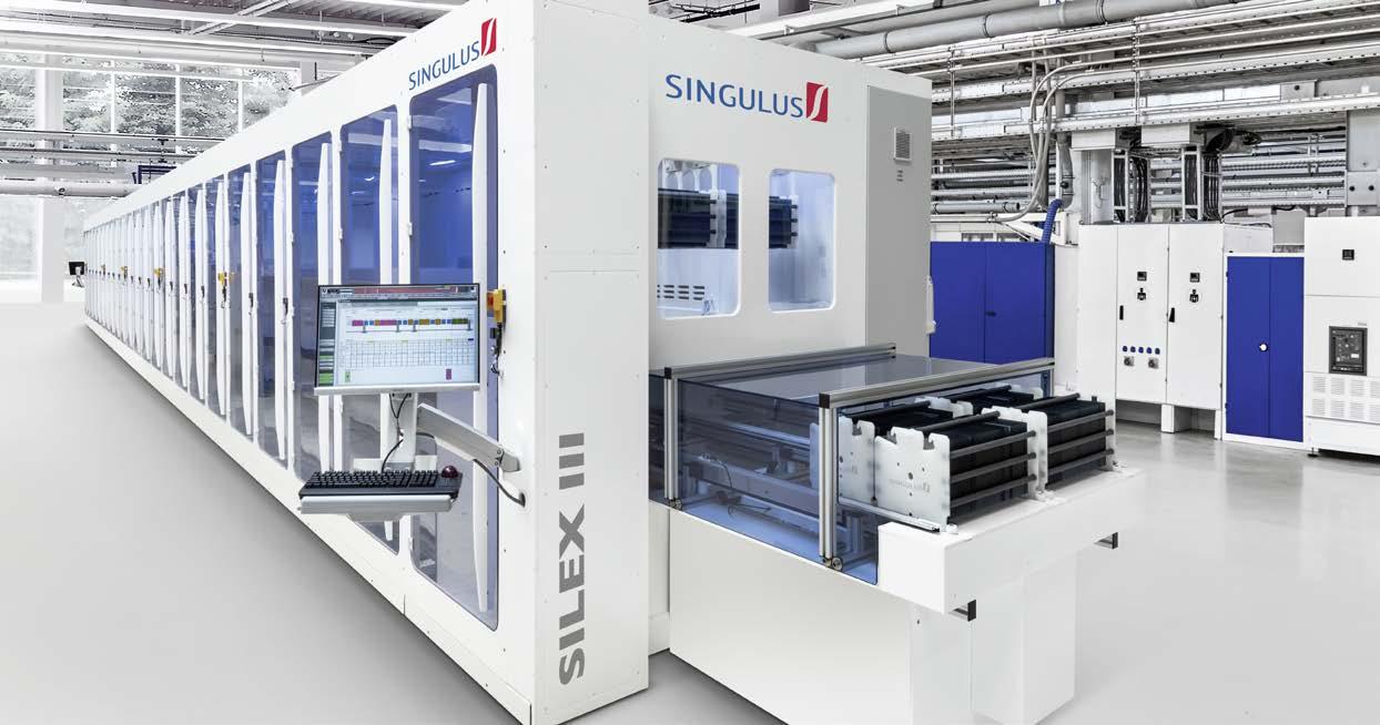
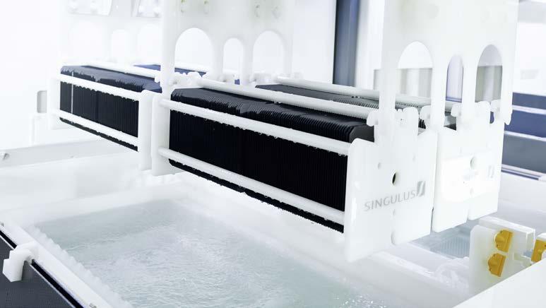
SINGULUS TECHNOLOGIES provides complete automated dry-in/dry-out solutions for wet-chemical treatments of Si-wafers in standard and highefficiency solar cell lines. The recently introduced modular SILEX III batch system offers a wide range of process options. With respect to highest flexibility in configuration, the SILEX III is characterized by a clear modular design and compact footprint.
The SILEX III was specially designed for high production volumes. With this mass production system, which can achieve up to 730 MW annual capacity and more, depending on cell efficiency, all wet chemical applications (batch) at the HJT, TOPCon and Perovskite cell concepts can be covered. The SILEX III system achieves an output starting up to 14,000 wph (gross), depending on wafer size.
The SILEX III combines common etching and cleaning steps of monocrystalline Si with advanced cleaning and conditioning processes.
The heart of the SILEX III is the alkaline texturing process improved and adapted to future demands through several years. SINGULUS TECHNOLOGIES guarantees a stable, mass production proven process, which can be used in all common and upcoming cell stacks. Different requirements like pyramid size and shape can be easily adjusted by the use of different additives and process parameters.
Efficient cleaning steps are an indispensable requirement to improve cell efficiencies and reduce operation costs. Ozone-based cleaning operations, applied on SILEX III wet bench, combine efficient organic and metal removal with an appropriate surface conditioning under high and stable ozone concentrations due to the self-developed
» Organic Cleaning
» Metal Cleaning
» Surface Conditioning
» Cascade Overflow
» Spray System
» Combination Rinse
» Hot/Cold Water Treatment
» Hot Air, N2 Drying
SINGOZON system. Due to low chemical costs and consumption, simple process control and high metal removal efficiency, ozonized cleaning baths are the perfect substitute for traditional, expensive multi-step RCA cleanings, known from the solar and semiconductor industry or even for the substitute of H2O2 based cleaning steps.
The ozone treatment can also be used in combination with HF for pyramid rounding, which achieves an optimal surface for passivation in HJT production lines and therefore an improvement of cell efficiency.
Alkaline chemical etch isolation is a PERC and TOPCon relevant process, which can be done, in combination with a prior single side inline HF step, in the SILEX III system. This results in an excellent polished, isolated wafer surface. With this development Singulus offers a HNO3-free, environmentally friendly option for etch isolation.
The SILEX III ALTEX is designed to apply IPA-free texturing processes, offering substantial cost advantages compared to traditional etching systems. This texturing process can be adjusted to the individual requirements of standard and advanced cell technologies.
» Alkaline Texturing
» Chemical Polishing/Thinning
» Metal and Oxide Etch
The SILEX III CLEAN is provided to run dedicated cleaning sequences for pre- or post-deposition processes. Depending on cell process flow and requirement the configuration can be designed individually, involving RCA or Ozone based cleanings as well as slight etching steps.
The SILEX GETTERING can be simple integrated in every mass production to be independent from wafer quality or/and for an additional boost in efficiency. By the use of a thermal, phosporous based Gettering process in combination with the SILEX III advanced etching step, it is possible to decrease impurities in the bulk material and improve the performance of silicon wafers.
» High throughput up to 14,000 wph gross; wafer size: up to G12
» High throughput for GW scale mass production
» Short, stable, and adjustable texturing process
» Low cost of ownership and high uptime
» Low breakage rate < 0.01 %
» Ozone-enhanced cleaning & etching
» Appropriate and effective rinsing and drying
» Individual, flexible process sequencing
» Onboard scheduler software for throughput and recipe tuning
» Onboard performance analyzer software
» Intelligent water-cascading for optimal rinsing quality by low water consumption
» Smart integration of different rinsing principles for decreasing of media carry over
» Ideal feed and bleed balance permits long bath lifetimes
» In-house carrier development
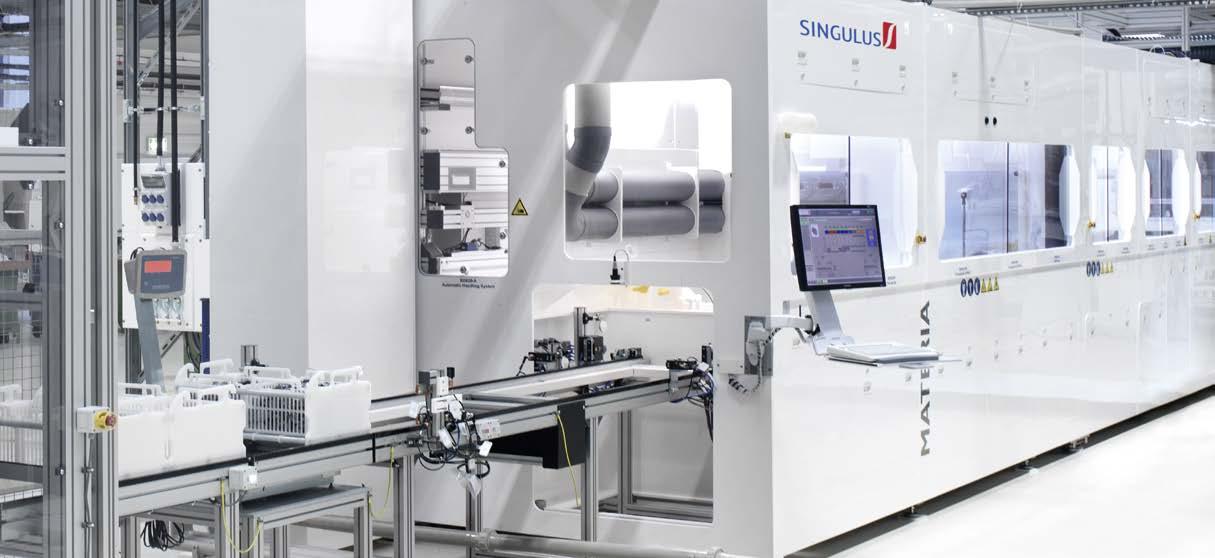
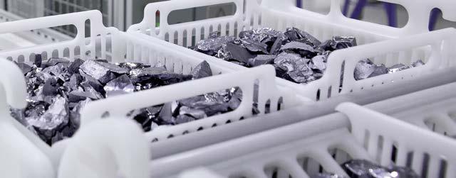
SINGULUS TECHNOLOGIES introduces the MATERIA platform, a cutting-edge solution for silicon raw material preparation. MATERIA is a batch system designed for the chemical etching, cleaning, and drying of mono and multi silicon chunks for solar and semiconductor applications. Engineered to meet the exacting purity standards of silicon production, MATERIA also prioritizes cost efficiency, making it a vital asset in industrial settings.
» Suitable for poly silicon (electronic, solar, or UMG grade)
» Accommodates to different chunk size sortings
» Throughput ranging up to 3,000 tons per annum (customizable upon request)
» Engineered for continuous operation: 24/7, 365 days a year
» High uptime availability
» Conforms to international safety standards
» Optional carrier return and management system (closed loop system), incl. interconnect to pre-and post-steps (e.g. packaging)
» Offers options for all state-of-the art processes for the efficient cleaning of poly chunks, along with multiple cleaning methods such as ozone cleaning, ultrasonic cleaning, and high-pressure spray
» Supports multi-recipe management via graphical user interface or Manufacturing Execution System (MES)
» Process support services available
» Advanced vacuum drying for a safe and stable drying of also highly packed poly chunk baskets
OPTIMIZED PROCESS BASKETS ENSURE
» Reduced drying time
» Minimal carry-over of water and acid residues
» Decreased freshwater and chemical consumption
» Continuous monitoring and tracking of consumption data
The MATERIA PCE stands as a versatile, efficient, and cost-effective solution, setting new standards in silicon cleaning technology for the solar and semiconductor industries.
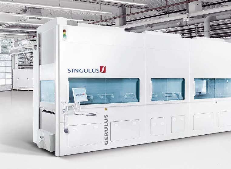
The GERULUS Wafer Block Pre-Clean & Deglue System represents a specialized solution utilized within the solar and semiconductor industries to meticulously clean wafer blocks of contaminants and effectively separate (deglue) them from their carrier system. Here is a detailed look at the features and functions of this system:
Technical Features
» Proven, highly integrated design tailored for efficiency
» High throughput capability ensures swift processing
» Engineered for continuous operation: 24/7, 365 days a year
» Exceptional availability with high uptime exceeding
» Incorporates an advanced pre-cleaning concept to optimize process outcomes and minimize processing times
» Fully compliant with international safety regulations
» Offers remarkable flexibility to accommodate diverse operational needs
» Designed for low cost-of-ownership with minimized freshwater consumption
» Utilizes a patented recycling system for sustainable resource management
» Minimized water consumption for eco-conscious operation
» System available for the degluing of different glue types
Cleaning Functions: : The system is adept at removing various contaminants encountered during the sawing process.
Carrier Material Separation: Integral to the process is the efficient separation of wafer blocks from their original carrier system, known as “degluing”, a critical step in preparing wafers for subsequent processing stages.
Automation: The GERULUS system boasts full automation, capable of handling a diverse range of wafer sizes and shapes. This automation ensures high throughput rates and streamlines production processes with precision and efficiency.
Process Flexibility: Flexibility is paramount, with the system offering a range of cleaning and separation options tailored to meet the specific requirements of different wafer sizes, carrier and glue types.
Quality Assurance: The system integrates robust quality assurance measures, including process monitoring functions, to guarantee that cleaned wafer blocks meet stringent purity and quality standards.
In summary, the GERULUS Wafer Block Pre-Clean & Deglue System plays a pivotal role in optimizing the cleaning and preparation of wafer blocks, thereby ensuring the superior quality and performance of the semiconductor components produced.
Full Solution Provider for HJT Production Lines from Design to Mass Production
» Greenfield or existing building integrated turn-key solutions for TOPCon or HJT solar cell lines
» Full-service provider – one contract, one general contractor
» Technology analysis for investment decisions
» Business case creation support (technical due diligence, risk assessment and furthers)
» Comprehensive engineering services for equipment-, automatization- and overall fab planning, including facility- and utility structure
» Project Management (technical & administration)
» Consulting/Support on building related questions (for line integration)
AVAILABLE HJT STANDARD CONFIGURATIONS
Throughput: 1 GW / 2 GW / 3 GW / 500 MW Pilot Line
Wafer Size: M10 - G12 | Full or Half-Cell Processing 1 GW 2 GW 3 GW
» Training of staff
» Equipment move-in, installation and production line interconnection
» Supply of state-of-the-art equipment
» Process transfer line ramp-up and production line hand-over
» Long-term process services, to provide process- and product technology roadmap for increase of cell efficiency and module power
» Partnership with tier 1 solar institutes for up-to-date product and process development
Wafer Inspection System Texturing & Cleaning
Subsidiaries
Your direct contact: www.singulus.com
Headquarters
SINGULUS TECHNOLOGIES AG
Hanauer Landstrasse 103 63796 Kahl, Germany
Tel. +49 6188 440-0 sales@singulus.de www.singulus.com
Subsidiaries
China
SINGULUS TECHNOLOGIES (SHANGHAI) Co. Ltd.
Tel. +86 21 61073997 sales@singulus.cn
SINGULUS TECHNOLOGIES
Guangzhou Office
Tel. +86 13822138376 sales@singulus.cn
France
SINGULUS TECHNOLOGIES
FRANCE S.A.R.L.
Tel. +33 3 89 31 11 29 sales@singulus.fr
North America
SINGULUS TECHNOLOGIES INC.
Tel. +1 860 683 8000 sales@singulus.com
South America
SINGULUS TECHNOLOGIES
LATIN AMERICA LTDA. Tel. +55 11 2165 2410 sales@singulus.com.br
South East Asia
SINGULUS TECHNOLOGIES
ASIA PACIFIC PTE LTD. Tel. +65 67411912 sales@singulus.com.sg
Taipei Office
SINGULUS TECHNOLOGIES
TAIWAN LIMITED
Tel. +886 2 8692 6996 sales@singulus.com.tw
SINGULUS TECHNOLOGIES - Thin-Film Coating and Surface Treatment
SINGULUS TECHNOLOGIES develops and assembles innovative machines and systems for efficient thin-film coating and surface treatment processes, which are used worldwide in the Photovoltaics, Semiconductor, Medical Technology, Packaging, Glass & Automotive as well as Battery & Hydrogen markets.
The company’s core competencies include various processes of coating technology (PVD sputtering, PECVD, evaporation), surface treatment as well as wet-chemical and thermal production processes.
SINGULUS TECHNOLOGIES sees sustainability as an opportunity to position itself with innovative products. In the focus are environmental awareness, efficient use of resources and avoidance of unnecessary CO₂ pollution.
SINGULUS TECHNOLOGIES attaches great importance to responsible and sustainable corporate governance.