technology in context
at increased transfer rates. To address this, the ONFI 3.0 NV-DDR2 interface requires tighter tolerances across process, voltage and temperature than the previous specification. Selectable drive strength settings of 18 ohms, 25 ohms, 35 ohms and 50 ohms are available on the NAND device. Warm-up cycles during data input or data output provide a configurable number of dummy cycles with no incremental data transfer. Signal integrity of the system is improved by reducing the effects of intersymbol interference (ISI).
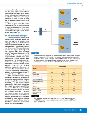
Bus 2
NAND Package 2 Bus 1
~5”
HOST
On-Die Termination Techniques
Termination improves noise margins, reduces signal reflections, affects slew rates, and improves the interface signal integrity overall. Figure 4 illustrates the signal integrity improvements with termination enabled. It can easily be observed that the aperture of the data window and the slew rate improve drastically—making it a picture that is worth a thousand words. When on-die termination (ODT) is enabled, the device or host can dynamically select when to switch on the termination circuitry to avoid unwanted power consumption. The termination circuitry on the die consists of a pull-up resistive element and a pull-down resistive element where RTTPU = RTTPD = 2 x RTT. RTT is the equivalent termination value selected for the device. For each individual die, the ONFI 3.0 specification can provide RTT values of 30 ohms (optional), 50 ohms, 75 ohms, 100 ohms and 150 ohms. While termination improves the signal integrity of the system, it comes at the possible cost of additional power consumption. For example, if a termination scheme requires RTT = 50 ohm, a single I/O could have 9 mA or more current consumption. For a single data channel on an SSD that may consist of 9 to 11 signals with ODT enabled, this could consume 160 to 180 mW. Because of these costs, it’s important that system designers use the minimum amount of termination to achieve the desired I/O performance. ONFI 3.0 provides flexibility to make intelligent termination tradeoffs dynamically and attain the best desired performance at the minimal amount of power consumption.
Bus 2
NAND Package 1 Bus 1
Figure 3 Single-channel SSD topology for signal integrity study: The SSD tree topology used to evaluate 400 MT/s NAND interface speeds includes a host controller connected to two NAND packages with four NAND Flash devices per package, for a total load of eight NAND devices or dies (LUNs) on the channel. SSD form factors determine the distance from host to NAND devices.
Data Interface Feature SDR
NV-DDR
NV-DDR2
SDR
DDR
DDR
-
200 MT/s
400 MT/s
CE_n Pin reduction support
Yes
Yes
Yes
Volume addressing support
Yes
Yes
Yes
On-die termination support
No
No
Yes
Differential signaling
No
No
Yes, optional for DQS and/or RE_n
3.3V or 1.8V
3.3V or 1.8V
1.8V
External VPP suport
Yes
Yes
Yes
External VREFQ support
No
No
Yes
Asynchronous
Source Synchronous
n/a
Protocol Maximum speed
VCCQ support
Previous name in older ONFI specifications
TABLE 1 Interfaces and features supported by ONFI 3.0: The newly developed NV-DDR2 interface is backward compatible with the previous SDR and NV-DDR interfaces.
RTC MAGAZINE OCTOBER 2011
21