technology in context
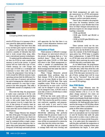
DRAM
NAND
PCM Fast
Sequential Read
Fast
Fast
Random Read
Fast
Slow
Fast
Sequential Write
Fast
Medium
Medium
Random Write
Fast
Slow
Medium
Power
High
Low
Low
No
Yes
Yes
Medium
Low
High
Nonvolatile Cost
TABLE 1 Comparing DRAM, NAND and PCM
ested in PCM since it is immune to bit errors caused by alpha particle radiation. Those designers who have been able to try out these parts report to us that they are pleased to find that the technology removes a number of obstacles they have had to work around when using older, more conventional memory technologies. To understand the enthusiasm designers have for PCM we must consider how memory is used in the system. A typical system will use both some type of nonvolatile memory for code storage and some type of RAM as a scratchpad and sometimes to store other code. In order to keep the programmer from having to work around the different memory types, operating systems hide the differences between each type of memory and perform the task of managing the volatile and nonvolatile memories in a way that is transparent to the other programs. This adds a considerable amount of complexity to the system. Even with this help, the programmer is under some constraint to fit the code into the read-only code space and the data into the read-write data space. If either code or data grows larger than the size of its memory, even by a single byte, the size of that portion of memory must be doubled at a significant price increase. In some cases this can be avoided in a PCMbased system. Phase Change Memory has changed the rules of the game. No longer must code and data be split between two fixed-size banks of NVM and RAM. Code and data may be contained within a single component. For small system designers this reduces chip count and power consumption. Designers of both large and small systems
16
MARCH 2010 RTC MAGAZINE
will appreciate the fact that there is no longer a fixed delineation between read/ write and read-only memory.
Intricacies of Flash
Flash memory is difficult to manage. One designer we interviewed referred to the process of managing flash as a “very involved dance.” Those who have designed with either NAND or NOR flash will attest to this. Flash management involves a number of considerations like wear leveling, read-while-write and bad block management that make this task extraordinarily complex. Phase Change Memories present considerably fewer problems than do flash designs. PCM is byte-alterable so there are no erase blocks as there are in both NAND and NOR flash. This vastly simplifies writes. Writes do not need to be preceded by an erase cycle—in PCM ones can be changed to zeros and zeros can be changed to ones. A PCM’s write is more like a write to a RAM than to either NAND or NOR flash. PCM has fast write cycles with no need for the erase required by NAND and NOR. This removes the need for a concurrent read/write capability, and programmers will rarely, if ever, need to write code to prevent reads from occurring near a recent write. PCM has random NOR-like or SRAM-like addressing that perfectly matches what the processor wants to see. Furthermore, PCM does not require the error correction used with NAND flash since all bits are guaranteed to contain the same data that was written into them. All the algorithms that are required to manage flash with wear leveling and
bad block management are quite simply unnecessary in a PCM environment. Some call PCM: “A firmware/software engineer’s perfect nonvolatile memory.” There is also a benefit to the programmer, since the boundary between code and data space is more flexible than it has been. In today’s designs each memory application requires its own unique memory topology, commonly: • NOR and SRAM • NOR plus NAND and SRAM or PSRAM • NOR or NAND plus DRAM or mobile SDRAM These systems rarely use the nonvolatile memory to store temporary data, and can never use the RAM to store code, since the contents of the RAM disappear upon power loss. PCM helps to simplify these configurations. A single PCM chip or a PCM-only array will store both code and data, often removing the need to pair a RAM chip with a nonvolatile chip. As an added bonus, the programmer need now worry only about the size of the code plus data, rather than about the code space and the data space as two separate areas. If the data space increases by a couple of bytes, perhaps there will be room that can be “borrowed” from the code space. This luxury is simply unavailable in a non-PCM topology.
How PCM Works
Phase Change Memory uses the changing state of a special material to determine whether a bit is a 1 or a 0. The phase change memory’s two states are “crystallized” and “amorphous.” Like a liquid crystal display blocks light or allows it to pass through, depending on a crystal’s orientation, the chalcogenide glass that is used for bit storage in a PCM either allows current to pass (when crystallized) or impedes its flow (when amorphous). Bits are changed from a crystalline state to an amorphous one via a tiny heater at each bit location that melts the glass then cools it in either a way to allow crystals to grow or to keep crystals from growing. A set pulse,raises the temperature to melt the glass and holds the temperature at that level for a time, ramping it down once crystallization has begun. A reset pulse