International Journal of Electrical and Electronics Research ISSN 2348-6988 (online) Vol. 8, Issue 2, pp: (6-13), Month: April - June 2020, Available at: www.researchpublish.com
SURVEY ON 2-TO-4 DECODER USING QUANTUM DOT CELLULAR AUTOMATA
1Ruchita Patil, Maniram Rawat
1Research Scholar, Electronics and Communication Engineering Dept, SRCEM, Gwalior India
2 Professors, Electronics and Communication Engineering Dept, SRCEM, Gwalior India pruchi1992@gmail.com, maniramrawatmits@gmail.com
Abstract: Quantum-dot cellular automata (QCA) are promising models in nanotechnology based on the single electron effects of quantum dots and molecules. The present study designs and simulates the basic elements or Combinational circuit. A 2-to-4 decoder has been designed and implemented before with the help of numbers of three-input majority voters and successfully implemented in QCA. The design and simulation of a new decoder circuit on QCA with minimum delay, area and complexity we will try to design, simulate and compare with previous designs. The design is optimized by considerably reducing the number of cell counts and QCA wire crossings. The decoder is more robust and enjoys single layer wire crossing, via clock phasing, which requires only one type of cell .we try to implement that the proposed decoder circuit performs equally well compared to existing decoder designs and performs better in case of previous coplanar decoder designs with enable input functionality in all aspects.
We are study and try to design our own circuitry to overcome issue on complex relation for designing a decoder circuit remove or less wire crossing or multi layer option here we understand the last function with help of Boolean function of decoder circuit and realize in single design For This purpose we allow to choose different methodology and design techniques. We have tried to study some of decoder circuit designs on the basis of simulation results to move forward with our own designs for the purpose. QCADesigner software is used to create a detailed layout and for circuit simulation. The circuits simulated using QCADesigner.
Keywords: Quantum Dot Cellular Automata, Nanotechnology, 2-to-4 decoder, QCADesigner 2.03.
I. INTRODUCTION
A motivation towards nanotechnology is due to the limitations of scaling down of MOS structure in CMOS technology, because the scaling down of MOS leads to an increase in operating powers and latency. The microelectronic industry is experiencing new challenges for continuing the Moore's law [1]. Therefore, new alternatives are introduced to overcome the physical problems of CMOS [2]. Also, at the same time there are numbers of problems like short channel effects, tunneling effects etc. have been discovered, which have encouraged the need to find an alternative of CMOS technology. A quantum-dot cellular automaton (QCA) is one of the alternative nanotechnologies that are proposed to overcome such problems and take over the CMOS circuit designs. It has attained considerable worldwide attentions due to its attractive characteristics such as ultra-high speed (THz), high device density, and low power consumption of digital circuits in comparison to current CMOS technologies based circuit designs. Decoders are important digital circuit, which is generally used for addressing random access memory arrays. They can also be design in Quantum-dot cellular automata (QCA) technology at Nano-scale. Previously, a number of decoder designs have been proposed, but no one are actually efficient. QCA is a new digital system for next generation [3–4]. Majority gate [4] and Inverter cell [4] are two main primitive logic gates for circuit designs in QCA nanotechnology. Till now various QCA based logic Circuits have been implemented [4–15]. Majority gate [4] and Inverter cell [4] has desirable features to implement logic for QCA. However, still the logic is not competent and research is continuous due to the current trends of complexity, power and area constraints. Majority gate & Inverter cannot reduce the circuit complexity and maximizes the device density in QCA circuits alone. These gates are not functionally complete to design all logic circuits. The main focus of all new techniques is to reduce circuit parameters and excels these major issues.
Page | 6 Research Publish Journals
International Journal of Electrical and Electronics Research ISSN 2348-6988 (online) Vol. 8, Issue 2, pp: (6-13), Month: April - June 2020, Available at: www.researchpublish.com
Decoder is the most frequent combinational component used in digital logic systems. The Decoder is a very useful electronic circuit that has uses in many different applications such as signal routing, data communications and data bus control applications. Based on this various arrangements of the QCA cells widespread range of QCA Decoder designs are realizable [5–15]. A number of QCA decoders have been designed and implemented with the help of three majority gates. For Example they have implemented a decoder without enable input based on 3 input majority gates, during the design of Look up Table, a part of combinational logic block (CLB) of field programmable logic array (FPGA). Aim of this research reducing the complexity of design structure by three input majority gate. This approach results in large unused area used which can be seen from comparison table. This presents the simple and effective layout design of decoder digital circuit without using the property of crossover in the layout that used higher power compare to single layer circuit that not use the crossover in the circuit that have enhanced the performance of several conventional designs in terms of power, area, clock delays and circuit complexity. The detailed comparison is of the proposed and conventional designs with regards to various characteristics are presented in the discussion.
RESERCH OBJECTIVES
To build up an approach/philosophy which decreases or remove the wire crossing and propagation delay adequately when contrasted with approaches/technique that have been proposed in past for decoder design outline.
To improve the Logical operation with less area decoder design circuit with powerfully change plan for various Boolean capacity as indicated by their execution in the circuit. So we can enhance the come about without utilizing additional natural.
Design and recreation of proposed decoder quantum cell structures without wire crossing or without multi layer design with help of techniques and technology to tradeoff between power, Area and speed of outlines
II. TECHNICAL AND BACKGROUND
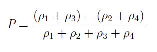
Quantum-Dot Cellular Automata (QCA) is another nano technology worldview which encodes twofold data by charge setup inside a phone rather than the regular current switches. There is no present stream inside the cells since the columbic cooperation between the electrons is adequate for calculation. This worldview gives one of numerous conceivable answers for transistor-less calculation at the nanoscale. The standard QCA cells have four quantum dots and two electrons [16]. There are different dots of QCA cells proposed which incorporate a six-dot QCA cell and an eight-dot QCA cell. In a QCA Cell, two electrons possess askew inverse spots in the cell because of shared shock of like charges. A case of a basic unpolarized QCA cell comprising of four quantum dots masterminded in a square is as appeared in Fig.1 dots are basically puts where a charge can be limited. There are two additional electrons in the cell those are allowed to move between the four dots. Burrowing in or out of a cell is smothered. The numbering of the dots in the cell goes clockwise starting from the dot on the top right.
Figure: -1 Simple 4-dot Unpolarized QCA cell.
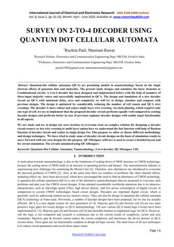
A polarization P in a cell, that measures the extent to which the electronic charge is distributed among the four dots, is therefore defined as:
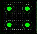
Where ρi is the electronic charge in each dot of a four dot QCA cell. Once polarized, a QCA cell can be in any one of the two possible states depending on the polarization of charges in the cell. Because of columbic repulsion, the two most likely polarization states of QCA can be denoted as P = +1 and P = -1 as shown in Fig.2. The two states depicted here are called most likely and not the only two polarization states because of the small (almost negligible) likelihood of existence of an erroneous state.
Page | 7 Research Publish Journals
International Journal of Electrical and Electronics Research ISSN 2348-6988 (online)
Vol. 8, Issue 2, pp: (6-13), Month: April - June 2020, Available at: www.researchpublish.com
Figure:-2 P = +1 Binary Logic1 P = - 1 Binary Logic 0
LOGICAL DEVICES IN QCA
As found in the past areas, the data in QCA cells is exchanged due to columbic cooperation’s between the neighboring QCA cells; the condition of one cell impacts the condition of the other.
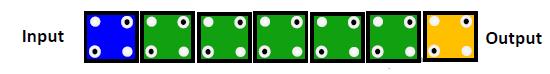
Binary Wire
A paired wire can be seen as an even arrangement of cells to transmit data starting with one cell then onto the next. A case of a QCA wire is as appeared in Fig. 3. A parallel wire is regularly separated into different clock zones, to guarantee that the flag doesn't fall apart as signs for the most part have a tendency to debase with a long chain of cells in a similar timing zone.
Figure: - 3 A QCA binary wire Realization
Inverter
Two diagonally aligned cells will have the opposite polarization. Henceforth, inverters can be implemented with lines of diagonally aligned cells. An example of a QCA Inverter is as shown in Figure
Figure: - 4 QCA designed inverter circuits
Majority Gate
Majority Gate (MV) is the fundamental logic block in any QCA design. A majority gate can be built with the help of five cells. The top, left and bottom cells are inputs. The device cell in the centre interacts with the three inputs and its result (the majority of the input bits) will be propagated to the cell on the right. An example of an MV representation in QCA is as shown in Figure 5. The logic function implemented by the MV is
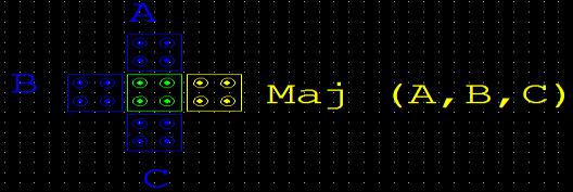

Consider the Coulombic cooperation between cells 1 and 4, cells 2 and 4, and cells 3 and 4. Coulombic connection between electrons in cells 1 and 4 would typically bring about cell 4 changing its polarization in light of electron aversion (accepting cell 1 is an info cell). Notwithstanding, cells 2 and 3 additionally impact the polarization of cell 4 and have polarization P=+1. Therefore, on the grounds that most of the cells impacting the gadget cell have polarization P=+1, it too will likewise accept this polarization on the grounds that the powers of Columbic collaboration are more grounded for it than for P=-1
Figure:-5 A three input majority gate
Page | 8 Research Publish Journals
International Journal of Electrical and Electronics Research ISSN 2348-6988 (online) Vol. 8, Issue 2, pp: (6-13), Month: April - June 2020, Available at: www.researchpublish.com
THE QCA CLOCK
This section will clarify and talk about how the QCA clockworks. Not at all like the standard CMOS clock, has the QCA clock had more than a high and a low stage. The periods of the QCA clock and illustrations are talked about underneath.
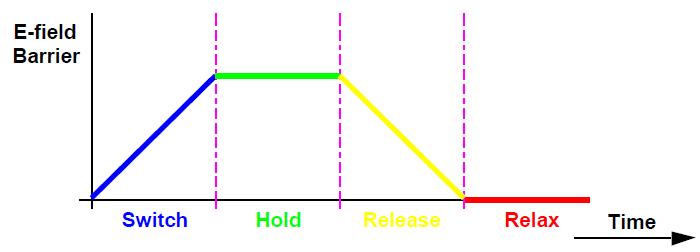
The check in QCA is multi-staged. Individual QCA cells are not planned independently. The wiring required to clock every phone exclusively could without much of a stretch overpower the disentanglement won by the natural neighborhoods interconnectivity of the QCA design [8] Four phase switching realized in each clocking phase for different clock zones. Information flows in a pipelined fashion from inputs towards outputs during four clock zones.
Figure: - 6 the four phases of the QCA clock
Now and time it merits specifying that there is some characteristic pipelining incorporated with the QCA innovation. After each 4 time steps, it is conceivable to put another esteem onto a QCA wire.
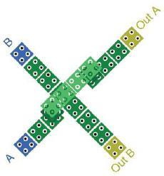
CROSSING
In QCA structures fabrication of interconnection between components needs to be handled efficiently for a better stability. Till now, there are two different types of crossover are available. These are coplanar and multilayer. In multilayer crossover, multiple layers are used as in CMOS circuit design for interconnection between components. In coplanar crossover strategy, wire crossing is done by two different cells. These cells are orthogonal to each other, so they operate without affecting neighboring cells. The first wire consists of cells of 900 orientations and second wire has only 450 orientations as shown in Figure 8. The main drawback of this scheme is that any misalignment of cells during fabrication may cause a cross coupling between the two wires. Works have been done to mitigate such effects, and also to increase the robustness of the circuits, but all these end up with large area overhead [14, 19].
Figure: - 7 Crossover diagram different orientation
III. PROBLEM IDENTIFICATION
In late year, numerous Researchers have proposed to Logic Gates compositional outline in Quantum Dot Cellular Automata neon-innovation applications by various procedures like traditional, when legitimately planned, can be over twice as quick as static rationale. It utilizes just the quicker Q-cell, which enhance region of rationale advancements. Static logic is slower on the grounds that it has double the capacitive stacking, higher limits, and uses dormant qubits for logic circuits. Rationale can be harder to with, however it might be the main decision when expanded handling speed is required. In regular CMOS rationale style, this rule can be rethought as an announcement that there is dependably a lowimpedance DC way between the yield and either the supply voltage or the ground
Page | 9 Research Publish Journals
International Journal of Electrical and Electronics Research ISSN 2348-6988 (online)
Vol. 8, Issue 2, pp: (6-13), Month: April - June 2020, Available at: www.researchpublish.com
In Logic Gate plans the spread deferral and vitality utilization of the Quantum Dot Cellular Automata are most basic issue when we enhance the delay than a similar time control utilization increments. Tradeoff between energy consumption and propagation delay by different– different methodology on the parameter of neon-technology. With this new methodology we improve both of them simultaneously without decreasing the basic characteristics of the circuit
DRAWBACKS
The power dissipation in this circuit is more than the traditional digital gates. However with same power consumption it performs faster.
But the use of substantial number of external fixed input results in high energy utilization, more power consumption and larger area.
The major problem of revisable gates is that it requires more area and quantum bit to process to realize. Thus, it will be more expensive to realize basic digital gates. Moreover if only standard logic gate we need in the circuit than that are not feasible for our design.
The power dissipation in this circuit is more than the traditional digital gates. However with less effective area, higher fan-out and same power consumption it performs faster.
But the use of substantial number of quantum cell in low input loads, more power consumption and small silicon area. But the use of substantial number of quantum cell in low input loads, more power consumption and small silicon area
IV. RELATED WORKS
In Beginning, previous designs of 2-to-4 decoder, which is already successfully implemented in QCA, are presented and then our design is proposed. Modular design methodology is first proposed in [31] to construct the 4-to-16 decoder. The latency of this decoder is only five clock cycles. The symmetrical fan out offers a solution to the problem where there is no wire crossing. There are five 2-to-4 decoders in a tree structure configuration to build a 4-to-16 decoder. This design uses AND, and delay (modular) blocks. Each decoder uses eight 2-input AND gates. Four of eight AND gates are used to enable or disable the output.
A new modular-based design methodology is presented for QCA. The basic block of QCA cells for logic computation is referred to as a tile. In general, a tile can have many different topologies in the QCA layout. For generating stable and synthesis-amenable logic functions, a tile must have the following features: (1) Logic functions must have flexible tile at high polarization level. It is necessary to have strong tile to limit interactions from unwanted external cells. (2) Signals should be routed easily between and among tiles (such as with a Manhattan strategy). (3) A tile should have stable signals, in which an output should not suffer from weakened value due to lack of polarization or the presence of a glitch. 3 × 3 QCA grid is an example of a tile. The tiles based on the 3 × 3 QCA grid provide universal logic functions and are flexible for logic design. The non-fully populated tile is defined as a tile in which one or more QCA cells are undeposited. The 2to-4 decoder using the 3 × 3 grid as part of the tile achieves a reduction in an area and in the number of clocking zones. A 4-to-16 decoder in [6] has five-layered structure. The inputs are placed in the middle layer (layer 3) and they move up and down. A recently designed 7 input majority gate is used as 4-input AND gate in the decoder design. For each different input, the decoder gives 16 different outputs (0–15), which address the memory cells. There is the same clock vertically in all layers due to layer clocking. The decoder of one clock cycle has less latency in comparison with other decoders. Higher input majority gates in multiple layers reduce the cell count and latency compared to other designs.
In [2], the circuit of the 2-to-4 decoder is designed using the 3-input majority gate in QCA. This circuit includes eight majority gates. A 5-input majority gate is needed for performing a logical 2-to-4 decoder [13] in QCA. Eight majority gates are required for increasing the delay and complexity in the circuit using traditional methods. The implemented decoder has four 5-input majority gates arrayed as AND. This circuit reaches the output in 7 clock phases (1.75 clock cycles) and includes two inputs and an enabled input. The decoder provides high consistency in the output and EN input makes it a controllable module.
Finally, in [1] it requires four 5-majority gates and two inverters as shown According to circuit. The decoder is composed of two separate blocks. The first block includes inputs and inverter gate, and the other block includes a five-input majority generates the output signal. Total of these blocks is implemented in a single layer design.
Page | 10 Research Publish Journals
International Journal of Electrical and Electronics Research ISSN 2348-6988 (online) Vol. 8, Issue 2, pp: (6-13), Month: April - June 2020, Available at: www.researchpublish.com
A decoder is imperative piece of memory, for address decoding and encoding. The scaling influences the gadget execution because of limitations like warmth dispersal and power utilization. A Quantum dot Cellular Automata (QCA) is a contrasting option to CMOS. In this venture propose a reversible gate based decoder design. It gives reversibility and area minimization. A QCA designer tool has been used to approve the execution of reversible decoders.
Table 1:- The list of previous single-layer 2-to-4 decoder
Design Cell count Area (μm2) Clock zones Layer(s)
Lantz and Peskin [31]] 318 0.5 7 1 Kianpour and Sabbaghi-Nadooshan [9] 270 0.38 7 1 Kianpour and Sabbaghi-Nadooshan [2] 268 0.3 7 1 Robab Sherizadeh, Nima Jafari Navimipour [1] 193 0.22 3 1
V. QCADESIGNER TOOL
Initially developed at the ATIPS Laboratory, University of Calgary, QCADesigner has attracted some important new developers, including top researchers from the University of Notre Dame. The project is written in C/C++ and employs a wide range of open-source software such as the GTK graphics library, and is maintained under the GNU public license for open source software. Developing the project in this manner enables it to be compiled and used on a wide range of systems. The objective of the project is to create an easy to use simulation and layout tool available freely to the research community via the Internet. One of the most important design specifications is that other developers should be able to easily integrate their own utilities into QCADesigner. This is accomplished by providing a standardized method of representing information within the software. As well, simulation engines can easily be integrated into QCADesigner using a standardized calling scheme and data types.
Programming bundles that plan, format, and help in the manufacture of incorporated circuits have disentangled the outline procedure and lessened an opportunity to-advertise for some circuits. Specifically, planning a circuit once for all creation advancements, rather than another outline for each assembling innovation, incredibly extended the extension and capacity of these outline devices. This detachment amongst engineering and innovation was effectively actualized by means of the Caltech Interchange Format or CIF [15]. Current QCA configuration devices have not yet built up a document arrange that backings the partition amongst engineering and innovation. Also, each plan device keeps on utilizing its own document arranges. Hence, a QCA circuit architect can't plan and reenact a similar circuit with different apparatuses without updating it each time.
Both of these restrictions have been removed in this thesis by developing a set of file formats for QCA circuit design. There are two formats dedicated to detailing the circuit architecture with no technology-dependent information contained in them. A third format has been created that contains the specific technology information used to implement a QCA circuit. These formats are based on the XML (eXtensible Markup Language) standard, thus, any design tool could be capable of using these file formats.
VI. CONCLUSION
In this paper we try to find an efficient 2-to-4 decoder, which is optimal in all aspects in comparison to other designs. We try to design that requires optimum number of cells and this reduction in number of cells makes the circuit more compact and stable, which enjoys its extension with other structures.
Research is also needed for using the design without wire crossing techniques in more complex circuits and the principal of using the dead computation time in clocking scheme should be exploited. Circuits that make use of clocking scheme can be designed and tested for efficiency in terms of power and performance.
REFERENCES
[1] Robab Sherizadesh, Nima Jafari Navipour. Designing a2-4-to4 decoder on nano-Scale based on quntum-dot cellular automata for energy dissipation improving.S0030-4026(17)31693-5;IJLEO 60177; https://doi.org/10.1016/j.ijleo 2017.12.055
[2] Lent, C.S., Bypassing the transistor paradigm. Science, 2000. 288(5471): p. 1597-1599.
[3] Kianpour, M. and R. Sabbaghi-Nadooshan, A conventional design and simulation for CLB implementation of an FPGA quantum-dot cellular automata. Microprocessors andMicrosystems, 2014. 38(8): p. 1046-1062.
Page | 11 Research Publish Journals
International Journal of Electrical and Electronics Research ISSN 2348-6988 (online) Vol. 8, Issue 2, pp: (6-13), Month: April - June 2020, Available at: www.researchpublish.com
[4] Mardoukhi, Y. and E. Räsänen, Optimal control of charge with local gates in quantum-dot lattices. The European Physical Journal B, 2014. 87(6): p. 144.
[5] Tougaw, D., J. Szaday, and J.D. Will, A signal distribution grid for quantum-dot cellular automata. Journal of Computational Electronics, 2016. 15(2): p. 446-454.
[6] Alkaldy, E., K. Navi, and F. Sharifi, A Novel Design Approach for Multi-input XOR Gate Using Multi-input Majority Function. Arabian Journal for Science and Engineering, 2014. 39(11): p.7923-7932.
[7] Ghosh, B., J.S. Chandra, and A. Salimath, DESIGN OF A MULTI-LAYERED QCA CONFIGURABLE LOGIC BLOCK FOR FPGAs. Journal of Circuits, Systems, and Computers, 2014. 23(06): p. 1450089.
[8] Sheikhfaal, S., et al., Designing efficient QCA logical circuits with power dissipation analysis. Microelectronics Journal, 2015. 46(6): p. 462-471.
[9] Seitz, C.L., System timing. Introduction to VLSI systems, 1980: p. 218-262.
[10] Kianpour, M. and R. Sabbaghi-Nadooshan. A novel modular decoder implementation in quantum-dot cellular automata (QCA). in Nanoscience, Technology and Societal Implications (NSTSI), 2011 International Conference on. 2011. IEEE.
[11] Afroz, S. and N.J. Navimipour, Memory designing using quantum dot cellular automata: systematic literature review, classification, and current trends. Journal of Circuits, Systems, and Computers, 2017.
[12] Seyedi, S. and N.J. Navimipour, An optimized design of full adder based on Nanoscale quantumdot cellular automata. Microprocessors and Microsystems, 2017.
[13] Sasamal, T.N., A.K. Singh, and A. Mohan, An optimal design of full adder based on 5-inputmajority gate in coplanar quantum-dot cellular automata. Optik - International Journal for Lightand Electron Optics, 2016. 127(20): p. 8576-8591.
[14] Navi, K., et al., A new quantum-dot cellular automata full-adder. Microelectronics Journal, 2010.41(12): p. 820-826.
[15] Orlov, A., et al., Realization of a functional cell for quantum-dot cellular automata. Science,1997. 277(5328): p. 928-930.
[16] Blair, E.P., E. Yost, and C.S. Lent, Power dissipation in clocking wires for clocked molecularquantum-dot cellular automata. Journal of computational electronics, 2010. 9(1): p. 49-55.
[17] Kianpour, M. and R. Sabbaghi-Nadooshan. A conventional design for CLB implementation of aFPGA in quantumdot cellular automata (QCA). in Proceedings of the 2012 IEEE/ACM International Symposium on Nanoscale Architectures. 2012. ACM.
[18] Bhanja, S., et al., QCA circuits for robust coplanar crossing. Journal of Electronic Testing, 2007.23(2-3): p. 193-210.
[19] Angizi, S., et al., Novel robust single layer wire crossing approach for exclusive or sum of productslogic design with quantum-dot cellular automata. Journal of Low Power Electronics, 2014. 10(2): p. 259-271.
[20] Das, J.C. and D. De, User Authentication Based on Quantum-Dot Cellular Automata Using Reversible Logic for Secure Nanocommunication. Arabian Journal for Science and Engineering, 2016. 41(3): p. 773-784.
[21] Das, J.C. and D. De, Operational efficiency of novel SISO shift register under thermal randomnessin quantum-dot cellular automata design. Microsystem Technologies, 2016: p. 1-14.
[22] Mohammadi, Z. and M. Mohammadi, Implementing a one-bit reversible full adder using quantum-dot cellular automata. Quantum Information Processing, 2014. 13(9): p. 2127-2147.
[23] Cho, H. and E.E. Swartzlander Jr, Adder and multiplier design in quantum-dot cellular automata.IEEE Transactions on Computers, 2009. 58(6): p. 721-727.
[24] Lent, C.S. and P.D. Tougaw, A device architecture for computing with quantum dots. Proceedingsof the IEEE, 1997. 85(4): p. 541-557.
Page | 12 Research
Publish Journals
International Journal of Electrical and Electronics Research ISSN 2348-6988 (online) Vol. 8, Issue 2, pp: (6-13), Month: April - June 2020, Available at: www.researchpublish.com
[25] Amiri, M.A., M. Mahdavi, and S. Mirzakuchaki. QCA implementation of a mux-based FPGA CLB.in Proc. Int. Conf. on Nanoscience and Nanotechnology. 2008.
[26] Timler, J. and C.S. Lent, Power gain and dissipation in quantum-dot cellular automata. journal ofapplied physics, 2002. 91(2): p. 823-831.
[27] Tougaw, P.D. and C.S. Lent, Dynamic behavior of quantum cellular automata. Journal of AppliedPhysics, 1996. 80(8): p. 4722-4736.
[28] Liu, W., et al., Are QCA cryptographic circuits resistant to power analysis attack? IEEEtransactions on nanotechnology, 2012. 11(6): p. 1239-1251.
[29] Srivastava, S., S. Sarkar, and S. Bhanja, Estimation of upper bound of power dissipation in QCA circuits. IEEE Transactions on Nanotechnology, 2009. 8(1): p. 116-127.
[30] Huang, J., et al. Simulation-based design of modular QCA circuits. in 5th IEEE Conference on Nanotechnology, 2005. 2005. IEEE.
[31] Walus, K., et al., QCADesigner: A rapid design and simulation tool for quantum-dot cellular automata. IEEE transactions on Nanotechnology, 2004. 3(1): p. 26-31.
[32] Lantz, T. and E. Peskin. A QCA implementation of a configurable logic block for an FPGA. in 2006 IEEE International Conference on Reconfigurable Computing and FPGA's (ReConFig 2006). 2006.
[33] Ma, X., J. Huang, and F. Lombardi, A model for computing and energy dissipation of molecularQCA devices and circuits. ACM Journal on Emerging Technologies in Computing Systems (JETC), 2008. 3(4): p. 3.
[34] Vetteth, A., et al. Quantum-dot cellular automata carry-look-ahead adder and barrel shifter. In IEEE Emerging Telecommunications Technologies Conference. 2002.
Page | 13 Research Publish Journals