International Journal of Electrical and Electronics Research ISSN 2348-6988 (online) Vol. 8, Issue 1, pp: (23-32), Month: January - March 2020, Available at: www.researchpublish.com
CARRY SAVE ADDER BY USING COPLANAR FULL ADDER WITHOUT INVERTER CHAIN DESIGN IN QCA
Umashankar Yadav1 , Umesh Barahdiya2
1Research Scholar, Electronics and Communication Engineering Dept, NITM, Gwalior India
2 Professors, Electronics and Communication Engineering Dept, NITM, Gwalior India 1uma624@gmail.com 2 umesh.baradia@gmail.com
Abstract: Quantum-dot cellular automata (QCA) are a new and promising computation paradigm, which can be a viable replacement for the complementary metal–oxide–semiconductor technology at nano-scale level. This technology provides a possible solution for improving the computation in various computational applications. It is expected that the CMOS technology reaches to the end of its road map because of many serious challenges such as short channel effect, impurity variations, high cost of lithography and more importantly, the heat. Quantum-dot cellular automata (QCA) are one of the alternative technologies that enable nano-scale circuit design with high performance and low power consumption features. In this aspect, QCA wire crossing is a challenging task in the coplanar QCA fabrication, as defects appear to be inherent due to two cell types in single layout structure. Some of previous design to introduce new approach for full adder design to full adder structure using an inverter chain. We have proposed a new low-complexity without using inverter chain to reduce circuitry requirement for extra Q-cell and power consumption repulsive geometry structural DUT, which consumes less Area compared to prior designs. To evaluate the usefulness of proposed design a new one bit full adder circuit and CSA with the help of basic full adder design presented. Our design achieves good improvement in cell count and consumes less area in comparison to the best single layer design. QCADesigner tool is used to validate the layout of the proposed designs. The usefulness of exhibited plans has been performed in QCADesigner form 2.0.3
Keywords: - QCA, Nano Technology’ QCA full adder, CSA, QCA Designer
I. INTRODUCTION
In coming years, reaching of CMOS technology to the end of its way is expected due to physical scalability, short channel effects (SCE), high cost of lithography and heating and cooling challenges. Therefore, the emerging technologies such as single electron transistor (SET), resonant tuning diode (RTD), carbon Nano tube field effect transistor (CNTFET) and quantum-dot cellular automata (QCA) can overcome the mentioned challenges. In the report summary of future technologies of international technology roadmap for semiconductor (ITRS), QCA has been introduced as an effective solution -. Due to its unique properties such as high speed, small size and low power consumption, this technology is one of the best options for designing high-density logical circuits. A square cell with four quantum dots located in its four corners is the simplest element in QCA technology. Based on the repulsion forces of columbic, the two electrons in this quantum cell are placed in the dots such that to minimize energy [4,5].
The International Technology Roadmap for Semiconductors (ITRS) has anticipated that size point of confinement of CMOS innovation will be constrained to around 5 nm to 10 nm and trusts this cutoff will be come to as ahead of schedule as 2017 [3]. The cutting edge processing devices are quantum PCs which depend on quantum mechanics. Quantum PCs depend on energy of photon and electron properties for performing figuring handling. They are parallel preparing that is a
International Journal of Electrical and Electronics Research ISSN 2348-6988 (online)
Vol. 8, Issue 1, pp: (23-32), Month: January - March 2020, Available at: www.researchpublish.com
great many operations at any given moment. So the preparing velocity of a 30 qubit quantum PC will be in the scope of TeraHertz (THz). The latest advances that is being examined. The circuits engaged with quantum based PCs can be produced from the quantum dot gates and circuits.
John von Neumann, a Hungarian mathematician presented the idea of cell automata. The possibility of quantum calculation is by and large included to Feynman who proposed a computational model in view of quantum mechanical laws. The discrete idea of cell mechanization and quantum mechanics prompts the development of nanoscale circuits to perform calculation. One conceivable approach to keep up the development in circuit density is to change from CMOS based worldview to nanoscale extends. The primary favorable circumstances of such circuits high speed, high design density, little measure of energy utilization and there by energy saving. A quantum dot cell automata (QCA) is a rising nanotechnology.
The paper is organized giving a review on QCA logic, structures, elementary concern about full adder design without using inverter chain and opportunity with QCA repulsive behavior to use in design aspect. Provides detail analysis about existing full adder mechanism. A new design of full adder and CSA its simulation along with physical proof, and. we present a glimpse of available full adder circuits and based on new architecture design, an efficient one bit full adder is proposed. Simulated results of proposed designs and comparison to previous works are inspected and finally paper concludes.
II. QCA FUNDAMENTALS
Quantum-Dot Cellular Automata (QCA) is another nano technology worldview which encodes twofold data by charge setup inside a phone rather than the regular current switches. There is no present stream inside the cells since the columbic cooperation between the electrons is adequate for calculation. This worldview gives one of numerous conceivable answers for transistor-less calculation at the nanoscale. The standard QCA cells have four quantum dots and two electrons [16]. There are different dots of QCA cells proposed which incorporate a six-dot QCA cell and an eight-dot QCA cell. In a QCA Cell, two electrons possess askew inverse spots in the cell because of shared shock of like charges. A case of a basic unpolarized QCA cell comprising of four quantum dots masterminded in a square is as appeared in Fig.1 dots are basically puts where a charge can be limited. There are two additional electrons in the cell those are allowed to move between the four dots. Burrowing in or out of a cell is smothered. The numbering of the dots in the cell goes clockwise starting from the dot on the top right.
Figure: - 1 Simple 4-dot Unpolarized QCA cell.
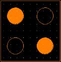
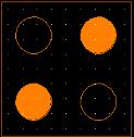
A polarization P in a cell, that measures the extent to which the electronic charge is distributed among the four dots, is therefore defined as:

Where ρi is the electronic charge in each dot of a four dot QCA cell. Once polarized, a QCA cell can be in any one of the two possible states depending on the polarization of charges in the cell. Because of columbic repulsion, the two most likely polarization states of QCA can be denoted as P = +1 and P = -1 as shown in Fig.2. The two states depicted here are called most likely and not the only two polarization states because of the small (almost negligible) likelihood of existence of an erroneous state.

International Journal of Electrical and Electronics Research ISSN 2348-6988 (online)
Vol. 8, Issue 1, pp: (23-32), Month: January - March 2020, Available at: www.researchpublish.com
III. LOGICAL DEVICES IN QCA
As found in the past areas, the data in QCA cells is exchanged due to columbic cooperation’s between the neighbouring QCA cells; the condition of one cell impacts the condition of the other. The essential rationale gadgets in QCA are:
Binary Wires.
Inverter.
Majority Gate Voter
Binary Wire: A paired wire can be seen as an even arrangement of cells to transmit data starting with one cell then onto the next. A case of a QCA wire is as appeared in Fig. 3. A parallel wire is regularly separated into different clock zones, to guarantee that the flag doesn't fall apart as signs for the most part have a tendency to debase with a long chain of cells in a similar timing zone.
Figure: - 3 A QCA binary wire Realization
Inverter: Two diagonally aligned cells will have the opposite polarization. Henceforth, inverters can be implemented with lines of diagonally aligned cells. An example of a QCA Inverter is as shown in Figure
Figure: - 4 QCA designed inverter circuits
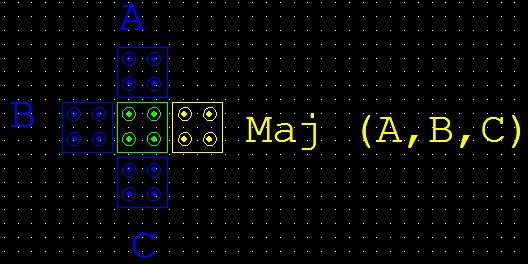
Majority Gate: Majority Gate (MV) is the fundamental logic block in any QCA design. A majority gate can be built with the help of five cells. The top, left and bottom cells are inputs. The device cell in the centre interacts with the three inputs and its result (the majority of the input bits) will be propagated to the cell on the right. An example of an MV representation in QCA is as shown in Figure 5. The logic function implemented by the MV is


Consider the Coulombic cooperation between cells 1 and 4, cells 2 and 4, and cells 3 and 4. Coulombic connection between electrons in cells 1 and 4 would typically bring about cell 4 changing its polarization in light of electron aversion (accepting cell 1 is an info cell). Notwithstanding, cells 2 and 3 additionally impact the polarization of cell 4 and have polarization P=+1. Therefore, on the grounds that most of the cells impacting the gadget cell have polarization P=+1, it too will likewise accept this polarization on the grounds that the powers of Columbic collaboration are more grounded for it than for P=-1.
Figure:-5 A three input majority gate
THE QCA CLOCK: This section will clarify and talk about how the QCA clockworks. Not at all like the standard CMOS clock, has the QCA clock had more than a high and a low stage. The periods of the QCA clock and illustrations are talked about underneath.
International Journal of Electrical and Electronics Research ISSN 2348-6988 (online)
Vol. 8, Issue 1, pp: (23-32), Month: January - March 2020, Available at: www.researchpublish.com
The check in QCA is multi-staged. Individual QCA cells are not planned independently. The wiring required to clock every phone exclusively could without much of a stretch overpower the disentanglement won by the natural neighbourhood interconnectivity of the QCA design [8]. Four phase switching realized in each clocking phase for different clock zones. Information flows in a pipelined fashion from inputs towards outputs during four clock zones.
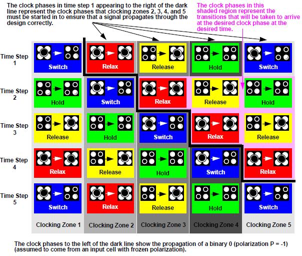
Figure: -
6
the four phases of the QCA clock
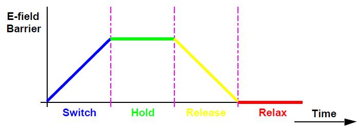
Figure:
- 7 Clocking phases in different clock Zones
Now and time it merits specifying that there is some characteristic pipelining incorporated with the QCA innovation. After each 4 time steps, it is conceivable to put another esteem onto a QCA wire.
CROSSING: For efficient design of QCA circuit in a smaller footprint, one area of primary consideration is wire crossing. Wire crossing is vital in QCA based plan and numerous strategies have been proposed to outline an efficient wire crossing, for example, coplanar based and the multilayer based methods, recently. Meanwhile the wire crossing strategies utilizing the control of clock stage have also been proposed [14]. Keeping in mind the end goal to outline the wire crossing using the said procedures, extra undertakings ought to be requested, for example, interpretation or rotation of QCA cells control of clock stage, expansion of bigger and soon. Like this their methods require extra time or spatial intricacy.
i) Coplanar based wire crossing procedure was proposed by Tougaw and Lent is shown in Fig. 8(a) basic geometry of the coplanar based wire crossing system [18, 19]. In this illustration the vertical wire and even wires are transmitting the values of 1 and 0 separately. To actualize this wire crossing the cell of horizontal wire are rotated by 45˚. On the off chance that the length of the vertical wire after a crossing point cell is adequate a transmitting value is not influenced by the other wire [14]. Likewise the horizontal wire should consist of odd number cells, since the property of the rotated cells has an inverter chain that the polarization substitutes heading between neighboring cells. Cells rotated by 45˚ initiate the extra space between cells. It inherently diminishes the energy partition between the ground state and the primary energized state which debases the execution of such a device as far as highest working temperature, protection from entropy, and least exchanging time [15].
ii) Multi layer based wire crossing strategy utilizes a hybrid crossover technique. This approach is similar to that of the coplanar based method from the perspective of the floor design since it would seem that appearance of two wires crossing. Truth be told, it comprises of the stereoscopic structure. In spite of the fact that this strategy has a few focal points, the noise issue between convergence cells in the hybrid territory is present [6]. There are additionally a few things to consider for plan and recreation forms in QCA Designer, for example, the quantity of layers, crossover and vertical cells [16].
International Journal of Electrical and Electronics Research ISSN 2348-6988 (online) Vol. 8, Issue 1, pp: (23-32), Month: January - March 2020, Available at: www.researchpublish.com
iii) QCA wire crossing is utilizing the different of clock system we consider the idea of QCA clock stage, for instance the information of present clock region is obtained from the past clock region. In this new technique each non neighboring clock area does not influence the inverse clock area. In this plan wire crossing depends on the distinction of 180˚ between two nonadjacent clock regions. However in this strategy a bit much of 45˚ rotation of cells utilized as a part of co planar wire intersection and sub layers courses of action as utilized as a part of multilayer wire crossing technique the nitty gritty wire crossing information appeared in Fig. 8(b) utilizes an inverse stage wire clock 0 and clock 2 and in Fig. 8(c) utilizes clock 1 and clock 3 wires used to information stream, the convergence cell can be have a place with any of two wires (either clock 0 or clock 2 in Fig. 8(b) and clock 1 or clock 3 in Fig. 8(c)) and there is no interface with each other.
Figure: - 8 Crossover diagram different orientation (a) Co Planar wire crossing; (b) wire crossing using clock 0 and clock 2; (c) wire crossing using clock 1 and clock 3
IV. LITERATURE REVIEW
Various QCA full-adders have been presented to date. The first one (presented in 1994) is composed of five three-input majority gates and three inverters (Tougaw and Lent, 1994). This full-adder uses QCA coplanar wire.
Hashemi et al. 181 crossing scheme. It is implemented in one layer using 192 QCA cells. In this design QCA clocking concepts are not considered. In Vetteth et al. (2002) another QCA full-adder using the same logical structure and coplanar wire crossing scheme is presented. In contrast to the previous design, this full-adder incorporates QCA clocking scheme and takes 14 clock phases (3.5 clock cycles) to generate outputs. This full-adder was used in designing a 4-bit CLA (Vetteth et al., 2002). A simpler QCA full-adder is presented in (Wang et al., 2003). This full-adder is composed of three three-input majority gates and two inverters (Wang et al., 2003). It uses QCA coplanar wire crossing scheme and takes 5 clock phases (1.25 clock cycles) to produce outputs. Hence, it is faster than presented design in (Vetteth et al., 2002). The schematic of this full-adder is shown in Figure 10. Different layouts for this schematic have been presented to date (Cho and Swartzlander, 2007, 2009; Cho, 2006; Hänninen and Takala, 2010; Kim et al., 2007; Zhang et al., 2005). The presented QCA full-adder in (Zhang et al., 2005) utilizes QCA multilayer wire crossing scheme and is simpler than previous design (Wang et al., 2003) in terms of cell count. It produces outputs in 4 clock phases (1 clock cycles); hence, it is faster than the previous designs. In the study of Cho and Swartzlander (2007) another QCA full-adder using the same logical structure and multilayer wire crossing scheme is presented. It takes 5 clock phases (1.25 clock cycles) to produce outputs. This full-adder was used to implement three kinds of adders (Ripple carry adder, carry look ahead adder and conditional sum adder) with large word sizes (Cho and Swartzlander, 2007). These adders were compared in terms of area, complexity (cell count) and delay (Cho and Swartzlander, 2007). Two other QCA full-adders (presented as Type I and II) using five gates (three majority gates and two inverters) are introduced in (Cho, 2006). This full-adder dominates all the previous designs in terms of area, complexity (cell count) and delay. In Hänninen and Takala (2010); Kim et al. (2007) robust QCA full-adders are presented. These designs use the coplanar wire crossing scheme for crossover wires. The presented design in (Hänninen and Takala, 2010) surpasses the presented design in (Kim et al., 2007) in terms of area, delay and complexity (cell count). Another QCA full-adder design is presented in (Rahimi et al., 2007). This adder is constructed using unconventional form of QCA cells. It is composed of two majority gates and one inverter. In this design in contrast to the previous structures, implemented using three-input majority gates, one of the majority gates is a five-input voter. In order to implement this schematic, a cubic design for QCA cells is presented in (Rahimi et al., 2007). This cubic cell has six sides and can be used to implement a five-input majority gate (Rahimi et al., 2007).

International Journal of Electrical and Electronics Research ISSN 2348-6988 (online)
Vol. 8, Issue 1, pp: (23-32), Month: January - March 2020, Available at: www.researchpublish.com
Finally the last one design based MV based 3-input XOR gate with inverter chain technique based on the cellular interaction is first proposed which consists of 61 cells and carry save adder using inverter chain 696 cells required
V. PROPOSED DESIGNS
In this section, a novel efficient full adder circuit in QCA nanotechnology is proposed. Our proposed design is implemented in one layer, without using inverter chain and has significantly lower number of quantum cells, less energy consumption and smaller area. This exploration could clear path for custom circuit designs which were not attainable in other processing advances. Our point is to happen upon with a reconfigurable design utilizing QCA which influences utilization of the dominant part to gate logical and the timing system which lessens the power significantly in contrast with the current models. The proposed technique recommends a viable answer for intelligent wiring with a lessened number or without of external fixed input cells giving certain values of info. In a run of the nano QCA circuit, both 0 and 1 fixed input are expected to execute functionality. The proposed strategy introduces certain value equipment which can lessen the quantity of required fixed inputs. In the same we avoid the multi layer and crossover circumstances in the design and all design are contracted in the single layer and single type of cells.
VI. PROPOSED 1-BIT FULL ADDER AND CSA
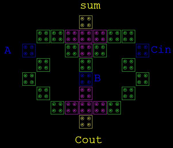
In this paper, we propose QCA full adder design there, we use a similar quantum cell technology to generate full adder desire result in a single layer formation with Boolean function satisfaction as per as full adder algorithm. Accordingly, by using this methodology, we design a new propose full adder design we have inputs A,B and Cin two output Carry and Sum who produce the two Boolean function, that is Carry = AB+BCin+ACin and second one is , As we seen in the diagram.
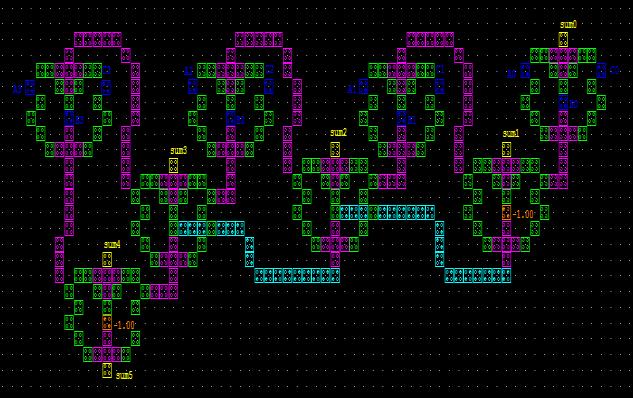
Design of one bit full adder, even larger bits and incorporating with least quantum cell uses because before this work many researchers to the great work on this, that’s by it is a challenging task for us. For such systems, the complexity increases in terms of number of quantum cell and wires crossing, so more prone to defects that occurs due to QCA fabrication of single layer crossing using two different cells (90˚ and 45˚) in a single layer layout. an optimal single layer QCA based full adder is designed and implemented using proposed geometric design, which incorporates the robust single layer crossing method using single cell (900) and case of carry save adder we use the same dull adder design to improvise the carry save adder design for pipeline methodology we require 8 full adder block and additional connecting circuitry here we totally avoided inverter chain method and minimize the less no of crossover with reference of previous one we did only 2 1-3 clock crossover rather than more than 10 inverter chin crossovers For implementation, Full adder block requires only 28 cells and CSA required 318 cells spreads over a lesser area. It consumes 3clock phases to produce valid carry output and Sum. The layout of the proposed full adder is shown in Fig. 9, and Carry Save Adder shown in Figure 10 which utilizes a coplanar 3-input majority gate and separate geometric design for generate Summing output The QCADesigner based simulation result for the proposed full adder. This indicates the correct operation of proposed structure and a valid output immediate clock cycle.
Figure 9 Layout of Propose Full Adder Design
International Journal of Electrical and Electronics Research ISSN 2348-6988 (online) Vol. 8, Issue 1, pp: (23-32), Month: January - March 2020, Available at: www.researchpublish.com
Figure 10 Layout of propose carry save adder
VII. SIMULATION RESULT AND ANALYSIS
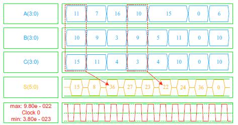
The simulation setup has been developed for two different functionality circuits design. The simulation has been performed on QCADesigner form 2.0.3 device these proposed circuits simulate and analyze the outcome on different parameters of quantum Dot cell automata technology.
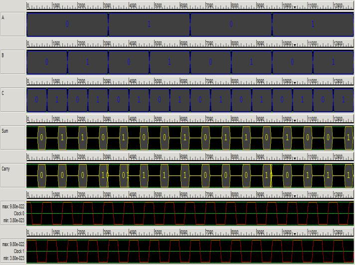
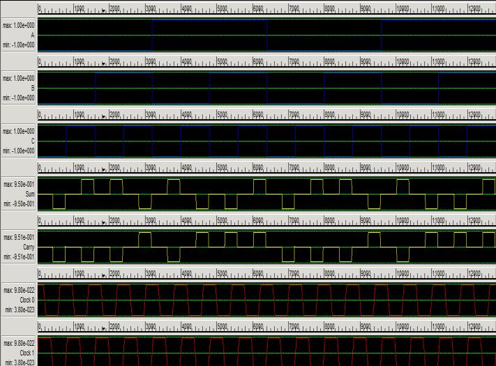
The measure of each QCA cell is set 18x18 nm with 5 nm width quantum dots. The parameters for a bistable estimate are as per the following: 0.001 convergence tolerance, 12.9 relative permittivity, 9.8e-22 J clock high, 3.8e-23 J clock low, 11.5 layer separation, and 100 maximum iterations per sample. The circuit design, generate the minimum supply voltage required to the tread-off between power and delay. The simulation results authenticate the correct operation of the proposed circuits. The reproduction comes about verify the right operation of the proposed circuits with all possible combination of full adder algorithm
International Journal of Electrical and Electronics Research ISSN 2348-6988 (online)
Vol. 8, Issue 1, pp: (23-32), Month: January - March 2020, Available at: www.researchpublish.com
Fig. 13 Simulation Wave form of Carry Save Adder Design
AREA AND CELL COUNT: In the past few sections, we have clearly explained how the proposed 1-bit full adder performs computation without any inverter chain compare to the previous designed digital full adder circuits. This gives us an enormous advantage with regard to power consumption and area as the number of QCA cells remains the less and CSA require only 318 cells only two 1-3 clock crossing. Tables depicting the area advantage posed by our design in comparison to existing adder are as shown in Tables
Table 1: Comparison result of Full Adder Design
Circuit Comp lexity (cell count)
Area (μm2)
Delay (cloc k cycle)
Cross wirin g Cost
Previous Full Adder[13] 111 0.13 2.75 yes 0.9831
Previous Full Adder[14] 93 0.09 1.25 yes 0.1406
Previous Full Adder[15] 79 0.07 1.25 yes 0.07
Previous Full Adder[16] 69 0.07 1 yes 0.07
Previous Full Adder[17] 63 0.05 1 yes 0.07 Previous Full Adder[18] 61 0.04 0.5 No 0.01 Prapose Full Adder 28 0.02 0.5 No 0.009
Table 1: Comparison result of Carry Save Adder Design
Circuit
Complexity (cell count) Area (μm2) Delay (clock cycle) Layer Type Cost
Kogge-Stone [19] 815 0.738 4 Multilayer 11.808 Ladner-Fischer [19] 698 618 4 Multilayer 9.888 CSA [20] 525 0.55 2.5 Multilayer 3.44 CSA [18] 696 0.66 2.25 Coplanar 3.34 Prapose CSA 318 0.53 2.25 Coplanar 2.24
VIII. CONCLUSION
In this work, an efficient full adder and CSA design has been proposed with physical and analytical proofs of design avoiding inverter chain method. To support this, a detailed analysis of structural, geographical and power issues of all prior ones and proposed full adder and CSA performed. To investigate area, fixed external inputs and clock used using QCADesigner 2.0.3 tool. To showcase the efficacy of the proposed designs, a new one bit full adder structure was introduced, which inculcates coplanar non-crossover wires, via clock phasing. It is observed that these coplanar structures are robust for considerable variation in temperature and CSA takes only two 1-3 clock crossover rather than more than 8 inverter chain crossings yield more compact digital circuits with respect to existing designs. The results confirmed that the presented structures have outperformed all prior designs and shows significant improvements in terms of power consumption, complexity, area occupation and input to output clock delay. Proposed optimal structures can lead to designing of more complex and high performance QCA nanoscale circuits in the future.
International Journal of Electrical and Electronics Research ISSN 2348-6988 (online) Vol. 8, Issue 1, pp: (23-32), Month: January - March 2020, Available at: www.researchpublish.com
Correlation examination of successful zones utilized and control use ultra low power Quantum Dot Cell with scaled cutoff voltage decreases latency delay and power usage with extensive sum. Impact of data vectors, Delay, power and supply voltage
Research is also needed for using the proposed custom wire crossing techniques in more complex circuits and the principal of using the less computation time in clocking scheme should be exploited. Circuits that make use of clocking scheme can be designed and tested for efficiency in terms of area, power and performance.
REFERANCEES
[1] C.S. Lent, P.D. Tougaw, W. Porod, G.H. Bernstein, Quantum cellular automata, Nanotechnology. 4 (1993) 49.
[2] T. John, C.S. Lent, Power gain and dissipation in quantum-dot cellular automata, J. Appl. Phys. 91 (2002) 823.
[3] H. Hosseinzadeh, S.R. Heikalabad, A novel fault tolerant majority gate in quantumdot cellular automata to create a revolution in design of fault tolerant nanostructures, with physical verification, Microelectron. Eng. 192 (2018) 52.
[4] J.C. Jeon, 7-input majority gate based priority encoder using multi-layer quantumdot cellular automata, Adv. Sci. Lett. 23 (2017) 10118.
[5] Y.W. You, J.C. Jeon, Design of one-bit comparator using multilayer in quantum-dot cellular automata, Adv. Sci. Lett. 23 (2017) 10087.
[6] N. Safoev, J.C. Jeon, Compact RCA based on multilayer quantum-dot cellular automata, Information Systems Design and Intelligent Applications, Springer, 2018, p. 515.
[7] S.R. Heikalabad, A.H. Navin, M. Hosseinzadeh, Content addressable memory cell in quantum-dot cellular automata, Microelectron. Eng. 163 (2016) 140.
[8] T.N. Sasamal, A.K. Singh, A. Mohan, An efficient design of quantum-dot cellular automata based 5-input majority gate with power analysis, Microprocess. Microsyst. (March 2018) 12. Article In press, Available online.
[9] F.P. Martineza, I. Farrer, D. Anderson, G.A.C. Jones, D.A. Ritchie, S.J. Chorley, C.G. Smith, Demonstration of a quantum cellular automata cell in a GaAsAlGaAs heterostructure, Appl. Phys. Lett. 91 (2007) 032102.
[10] F. Ahmad, G.M. Bhat, H. Khademolhosseini, S. Azimi, S. Angizi, K. Navi, Towards single layer quantum-dot cellular automata adders based on explicit interaction of cells, J. Comput. Sci. 16 (2016) 8.
[11] K. Walus, T.J. Dysart, G.A. Jullien, R.A. Budiman, QCADesigner: a rapid design and simulation tool for quantumdot cellular automata, IEEE Trans. Nanotechnol. 3(2004) 26.
[12] S. Srivastava, S. Sarkar, S. Bhanja, Estimation of upper bound of power dissipation in QCA circuits, IEEE Trans. Nanotechnol. 8 (2009) 116.
[13] D. Abedi, G. Jaberipur, M. Sangsefidi, Coplanar full adder in quantum-dot cellular automata via clock-zone-based crossover, IEEE Trans. Nanotechnol. 14 (2015) 497.
[14] S. Angizi1, E. Alkaldy, N. Bagherzadeh, K. Navi, Novel robust single layer wire crossing approach for exclusive or sum of products logic design with quantum-dot cellular automata, J. Low Power Electron. 10 (2014) 259.
[15] S. Hashemi, K. Navi, A novel robust QCA full-adder, Procedia Mater. Sci. 11 (2015) 376.
[16] M. Kianpour, R.S. Nadooshan, K. Navi, A novel design of 8-bit adder/subtractor by quantum-dot cellular automata, J. Comput. Syst. Sci. 80 (2014) 1404.
[17] A.A. Shaf, A.N. Bahar, Optimized design and performance analysis of novel comparator and full adder in nanoscale, Cogent Eng. 3 (1) (2016).
[18] Sarvarbek Erniyazov, Jun-Cheol Jeon, Carry save adder and carry look ahead adder using inverter chain based coplanar QCA full adder for low energy dissipation, Microelectronic Engineering 211 (2019) 37–43, https://doi.org/10.1016/j.mee.2019.03.015
International Journal of Electrical and Electronics Research ISSN 2348-6988 (online) Vol. 8, Issue 1, pp: (23-32), Month: January - March 2020, Available at: www.researchpublish.com
[19] V. Pudi, K. Sridharan, Low complexity design of ripple carry and Brent–kung adders in QCA, IEEE Trans. Nanotechnol. 11 (2012) 105.
[20] D. De, J.C. Das, Design of novel carry save adder using quantum dot-cellular automata, J. Comput. Sci. 22 (2017) 54.
[21] H. Cho, E.E. Swartzlander, Adder and multiplier design in quantum-dot cellular automata, IEEE Trans. Comput. 58 (2009) 721.
[22] H. Cho, E.E. Swartzlander, Pipelined carry lookahead adder design in quantum-dot cellular automata, Proc. IEEE Conf. Signals, USA (2005) 1191.
