Solution Manual for CMOS Digital Integrated Circuits
Analysis and Design 4th Edition Kang Leblebici Kim
ISBN 0073380628 9780073380629
Full link download: https://testbankpack.com/p/solution-manual-for-cmos-digitalintegrated-circuits-analysis-and-design-4th-edition-kang-leblebicikim-isbn-0073380628-9780073380629/
Exercise Problems
3.1 Consider a MOS system with the following parameters:
a. Determine the threshold voltage VT0 under zero bias at room temperature (T = 300 K).
that
3.97 0 and si 11.7 0 SOLUTION
First, calculate the Fermi potentials for the p-type substrate and for the n-type polysilicon gate:
The gate oxide capacitance per unit area is calculated using the dielectric constant of silicon dioxide and the oxide
Now, we can combine all components and calculate the threshold voltage.
18
tox 1.6nm GC 1.04V N A =2.8 10 18 cm -3 Q OX q 4 10 10 C/cm 2
Note
ox
:
kT ni 10 F (substrate) ln 0.026V ln 1 45 10 0.49V N q A 2.8 10 The depletion region charge density at VSB = 0 is found as follows: QB 0 2 q N A Si 2 F (substrate) 2 1.6 10 19 (2.8 1018 ) 11.7 8.85 10 14 2 0.49 9.53 10 7 C/cm2
oxide-interface
is: Qox q Nox 1.6 10 19 C 4 1010 cm-2 6.4 10 9 C/cm2
tox ox 3.97 8.85 10 14 F/cm C t ox ox 1.6 10 7 cm 2.2 10 6 F/cm2
The
charge
thickness
b Determine the type (p-type or n-type) and amount of channel implant (NI/cm2) required to change the threshold voltage to 0 6V
VT 0 GC 2 F (substrate) QB 0 Qox C C ox ox 1.04 ( 0.98) ( 0.53) (0.03) 0.44V
3.2 Consider a diffusion area that has the dimensions 0.4 m 0.2 m and the abrupt junction depth is 32 nm Its n-type impuritydoping level is N D =2 10 20 cm-3 and the surroundingp-type substrate doping level is N A =2 10 20 cm-3 Determine the capacitance when the diffusion area is biased at 1 2V and substrate is biased at 0V. In this problem, assume that there is no channel-stop implant
3.3 Describe the relationship between the mask channel length, LM, and the electrical channel length, L. Are they identical? If not, how would you express L in terms of LM and other parameters? SOLUTION :
The electrical channel length is related to the mask channel length by:

Where LD is the lateral diffusion length

I 14 19 SOLUTION : p-type implanted needed in the amount of: V 0.6 VT0 0.6 0.44 1.04 qN 1.04 C C ox 1.04 2.2 10 6 NI ox q 1.6 10 19 1.43 1013 cm-2
SOLUTION : C j (V ) A si q NA ND 1 2 NA ND 0 V kT ln N A N D 0.026 ln 2 1020 2 1020 1.21 0 q n 2 (1.45 1010 )2 i A 0.2 0.4 2 0.2 0.032 2 0 4 0.032 1.18 10 9 [ cm2 ] C j (V ) 1 1810 9 11.7 8.854 10 1.6 10 2 2.18 10 15[F] 4 10 40 20 4 10 1 1.21 1.2
L LM 2LD
3.4 How is the device junction temperature affected by the power dissipation of the chip and its package? Can you describe the relationship between the device junction temperature, ambient temperature, chip power dissipation and the packaging quality?
SOLUTION :
The device junction temperature at operating condition is given as T j Ta Pdiss , where Ta is the ambient temperature; Pdiss is the power dissipated in the chip; is the thermal resistance of the packaging A cheap package will have high which will result in large and possiblydamaging junction temperature. Thus the choice of packaging must be such that it is both economic and pretective of the device.
3.5 Describe the three components of the load capacitance Cload , where a logic gate is driving other fanout gates.
SOLUTION :
The three major components of the load capacitance are interconnect capacitance, the next stage input capacitance, i e., the gate capacitance and the drain parasitic capacitances of the current stage.
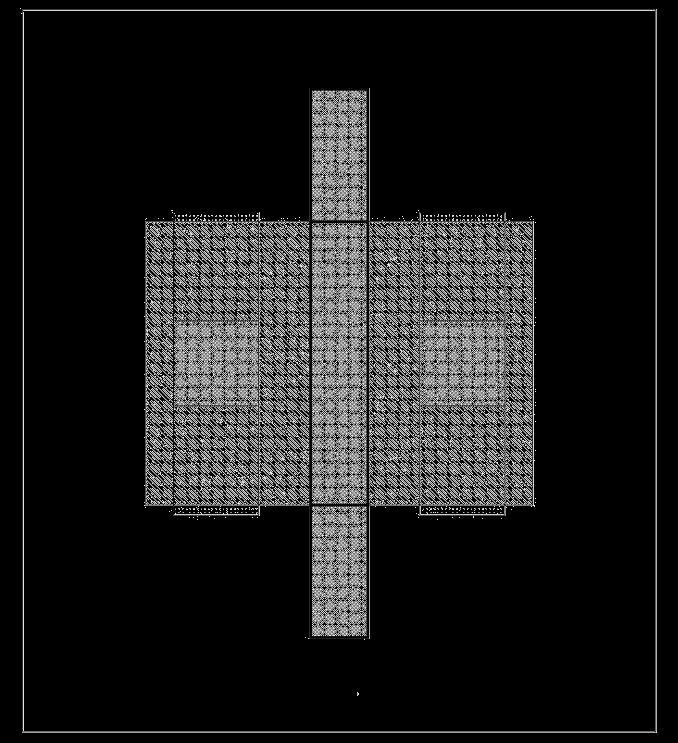
3.6 Consider a layout of an nMOS transistor shown in Fig P3 6 The process parameters are:
stop doping 16.0 ( p type substrate doping)
Find the effective drain parasitic capacitance when the drain node voltage changes from 1 2V to 0 6V.
ND 2 10 20 cm 3 NA 2 10 20 cm 3 X j 32nm LD 10nm tox 1.6nm VT 0 0.53V Channel


2 Y=6μm Wn =10μm GND n+ Output n+ Figure P3.6 SOLUTION : kT N N 0 ln A D 0.026 ln 2 1020 2 1020 10 2 1.21 q ni (1.45 10 ) kT N ' N 16 2 1020 21020 A D osw ln 2 0.026 ln 10 2 2.31 q ni (1.45 10 ) C j 0 si q NA ND 1 N N 2 A D 0 11.7 8.854 10 14 1.6 10 19 1020 2.61 10 6 [F/cm 2 ] 2 1.21 N C josw si q A ' ND 1 ' N 2 N A D osw 11.7 8.854 10 14 1.6 10 19 1.88 1020 2.59 10 6 [F/cm 2 ] 2 2.31
3.7
C jsw X j C josw 32 10 9 2.59 10 6 0.083[pF/cm] A Y W 6 10 60[ m2 ] P 2(Y W ) 2(6 10) 32[ m] 5 0 0 2.5 K 2 eq 0 5 2.5 2 0.8967 5.8967 3.3967 0.44 2.5 5 2.5 K ' 2 0 0 eq 0 5 2.5 2 0.8967 5.8967 3.3967 0.44 2.5 C drain Keq Cj 0 A Keq ' Cjsw P 0.44 9.6 10 9 60 10 8 0.46 1.847 10 12 32 10 4 5.25[ fF ]
the data, find : (a) the threshold voltage VT0 and, (b) velocity saturation vsat Some of the parameters are given as: W=0.6 m, EcL=0.4 V, , tox = 16 Å, |2 F| = 1.1 V VGS (V) VDS (V) VSB (V) ID( A) 0.6 0.6 0.0 6 0.65 0.6 0.0 12 0.9 1.2 0.3 44 1.2 1.2 0.3 156
A set of I-V characteristics for an nMOS transistor at room temperature is shown for different biasing conditions. Figure P3.7 shows the measurement setup
Using
SOLUTION : (a)
First, the MOS transistor is on (ID > 0) for VGS > 0 and VDS > 0. Thus, the transistor must be an nchannel MOSFET Assume that the transistor is enhancement-typeand, therefore, operating mode.
When VGS and VT are similar, velocity saturation terms are neglected Let (VGS1, ID1) and (VGS2, ID2) be any two current-voltagepairs obtained from the table. Then, the VT0, can be calculated.
3.8 Compare the two technologyscaling methods, namely, (1) the constant electric field scaling and (2) the constant power supply voltage scaling In particular, show analytically by using equations how the delay
D sat ox GS 1 T 0 I D 0 V ID VDS VGS VSB
Figure P3.7
I W
C (V V )2 (V GS T GS T c
v
I D1 I 6 A 0 65V 0 6V (V V )2 V 12 A 0 48V (b) D 2 (VGS 2 VT 0 )2 T 0 6 A 1 12 A Find velocity saturation C ox 3.9 8 85 10 14 216 10 4 F / m t ox ox 0 16 10 8 (V V )2 GS T c 12 0.6 10 6 vsat 216 10 6 v 0 172 0 17 0 4 (1 0 05 0 6) sat 1.06 106 m / s
time, power dissipation, and power density are affected in terms of the scaling factor, S. To be more specific, what would happen if the design rules change from, say, 1 μm to 1/S μm (S>1)?
3.9 A pMOS transistor was fabricated on ann-type substrate with a bulk doping density of N 1 1016 cm 3 ,gate doping density (n-type poly) of N
10 20 cm
,
the threshold voltage at room temperature for V
i 10 q n
SOLUTION : Const E field Const VDD W , L ,tox 1/ S 1/ S V 1/ S 1 DD C S S ox C CoxWL 1/ S 1/ S k n , kp S S I 1/ S S DD t C V delay I DD 1/ S 1/ S2 Power I DDVDD 1/ S2 S Power 1 S3 Power density Area
D D
3
Q
q 4
and gate oxide thickness of
ox 1.6nm
Use si 11.7 0 SOLUTION : N F ( substrate) kT ln D ,sub 0.026 ln 1 1016 0.348[V] q n 1.45 10 N 20 F ( gate) kT ln D , poly 1 10 0.026ln 0.587[V] 10 1 45 10 i GC F ( substrate ) F ( gate) 0.348 0.587 0.239[V] Cox ox 3 9 8.85 10143.45 10 8 [F/cm2 ] tox 0.1 10 4
/
1010 cm 2 , ox
t
Calculate
SB=0
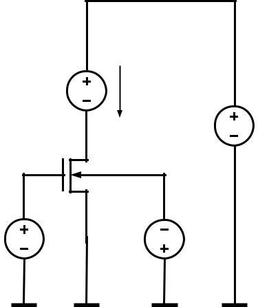
3.10 Using the parameters given, calculate the current through two nMOS transistors in series (see Fig P3 11), when the drain of the top transistor is tied to VDD, the source of the bottom transistor is tied to VSS = 0 and their gates are tied to VDD The substrate is also tied to VSS = 0 V Assume that W/L = 10 for both transistors and L=4 m
k' = 168 A/V2
VT0 = 0 48 V = 0.52 V1/2
|2 F| = 1 01 V
Hint : The solution requires several iterations, and the body effect on thresholdvoltage has to be taken into account. Start with the KCL equation
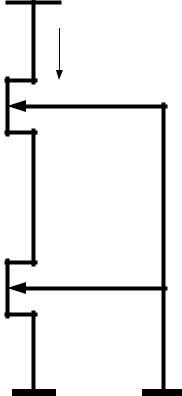
Figure
SOLUTION :
Q 2 qN B 0 2 D ,sub si F 2 1.6 10 19 1016 11.7 8.85 10 14 2 0.348 4.8 10 8 [C / cm2 ] V 2 T 0 GC Q B 0 F C ox Q ox C ox 8 10 19 0.239 2 0.348 4.8 10 4 10 1.6 10 2.51[V] 3.45 10 8 3.45 10 8
1 V ID= ? +1 V
P3 10
Since gate voltage is high, the midpoint Vx is expected to be low. Therefore, the load is in saturation and the driver is in linear region From KCL
Using the following two equations to iterate find the solution
The intermediate values are listed in the table:
3.11 The following parameters are given for an nMOS process:
(a) Calculate VT for an unimplanted transistor.
(b) What type and what concentration of impurities must be implanted to achieve VT = + 0 6 V and VT = – 0.6 V ?
1 V ID= ? +1 V Vx
Figure P3 10
1 2 k ' W I I D D , driver I D , load L L 1 Vx VT , L (Vx ) 2 1 2 k ' W 2 1 VT 0 Vx Vx 2
1 Vx VT ,L (Vx ) 2 1.04Vx Vx 2 V (V ) 0.48 0 52 1.01 V 1.01 T ,L x x
VT,L(Vx) Vx 0 480 0 1523 0 518 0 1337 0 513 0 1359 0.514 0.1357 0 514 0 1357 1 W 2 2 I D 2 k ' L (1.04Vx Vx ) 0.5 168 10 1.04 0.1357 0.1357 103.1[ A]
tox =
Å substrate doping NA = 4 1018 cm-3 polysilicon gate doping ND = 2 1020 cm-3 oxide-interface fixed-chargedensity Nox = 2 1010 cm-3
16
Negative charges needed in this case, so it must be p-type implant in the amount of
positive
need, must be n-type
18 D N t ox SOLUTION : (a) For unimplanted transistor, kT ni 10 F ( substrate) ln 0.026V ln 1 45 10 0.51V q kT N A 4 10 , poly 2 1020 F (gate) ln 0.026V ln q ni 10 1.45 10 0.61V GC F (substrate ) F (gate) 0.51V 0.61V 1.12V QB 0 2 q N A Si 2 F (substrate) 2 1.6 10 19 (4 1018 ) 11.7 8.85 10 14 2 0.51 1.16 10 6 C/cm2 ox 3.97 8.85 10 14 F/cm C ox 1.6 10 7 cm 2.2 10 6 F/cm2 V T 0 GC 2 (substrate) F QB 0 C ox Q ox C ox (b) For VT= 2V; 1.06 ( 1.12) ( 0.53) (0.03) 0.56V V 2 V T T 0 Q II 0.56 C ox Q II C ox
QII qN I (VT VT 0 )Cox NI (2 0.56) 2.2 10 6 13 3 1.610 19 1.98 10 cm For VT=-2V,
implant, 2.2 10 6 13 3 NI (2 0.56) 1.610 19 3.52 10 cm
VT0, k, ,
F = –1.1 V and L=4 m VGS (V) VDS (V) VBS (V) ID( A) 0.6 0.8 0 8 0.8 0.8 0 59 0.8 0.8 -0.3 37 0.8 1.0 0 60 SOLUTION :
charges
3.12
Using the measured data given, determine the device parameters
and assuming
Because the given device is a long channel device, when VDS≥VGS, the transistor operates in s aturation region, therefore

a) Find
b) Find V
c)
d) Find : From Row3 data,
3.13 Using the design rules specified in Chapter 2, sketch a simple layout of an nMOS transistor on grid paper. Use a minimum feature size of 60 nm. Neglect the substrate connection After you complete the layout, calculate approximate values for Cg, Csb, and Cdb The following parameters are given
depth = 32 nm
W = 300 nm L = 60 nm
ox = 1 6 nm
Sidewall doping = 4·109 cm-3 Drain bias = 0 V
I DSAT k 2 VGS VT 2 1 VDS I DSAT Row 4 1 VDS Row4 1 60 I DSAT Row 2 1 VDS Row2 1 10.8 59
Find k: From Row2 data,
0.09 V I DSAT Row 2 0.8 VT0 2 I DSAT Row1 0.6 VT 0 2 VT0=0.48V k 59 2 0.8 0.48 2 1 0.09 0.8 k 1.08 mA/V2 37 1075 2 0.8 VT (VBS 0.3) 2 1 0.09 0.8 VT (VBS0.3) 0.55 V 0.55 0.48 0.3 1.11.1 0.52 V1/2
Substrate doping NA = 4 1018 cm-3 Drain/source doping ND = 2 1020 cm-3
t
Junction
SOLUTION :
Because the drain bias is equal to 0V, there is no current in the device. First of all, Cox is calculated like below:
2 A
ox 3.97 8.85 10 14 F/cm C t ox ox 1.6 10 7 cm 2.2 10 6 F/cm2
total gate capacitance Cg is C C C C g gb gd gs CoxWL CoxWLD CoxWLD C WL ox ( total length) 2.2 10 2 F/m 2 300 10 9 m 60 10 9 m 0.396fF kT N N 0 ln A D 0.026V ln 4 1018 2 1020 20 1.11V n q i 2.1 10 kT N 0sw ln q (sw) N D 2 ni 0.026V ln 4 109 2 1020 20 2.1 10 0.57V
So
The zero-bias sidewall junction capacitance per unit length can also be found as follows
total area of the n the channel region /p junctions is calculated as the sum of the bottom area and the sidewall area facing
3.14 An enhancement-typenMOS transistor has the following parameters:

C j 0 Si q NA ND 1 N N 2 A D 0 11.7 8.85 10 14 F/cm 1.6 10 19 4 1018 2 1020 1 2 54.1 10 8 F/cm2 C 18 4 10 20 2 10 1 11V j 0sw Si q NA ND 1 N N 2 A D 0 11.7 8.85 10 14 F/cm 1.6 10 19 4 109 2 1020 1 24.1 10 12 F/cm2 9 2 4 10 2 10 20 0.57V
C jsw C j 0sw xj 24.1 10 12 F/cm2 32 10 7 cm 77.15aF/cm +
A (0.3 0.15) m2 (0.15 0.032) m2 0.05 m2 P 2 0.3 m 0.15 m 0.75 m C db A C j 0 P C jsw 0.05 10 8 cm2 54.1 10 8 F/cm2 0.75 10 4 cm 77.2 10 18 F/cm 0.271 10 15 F 0.271fF Csb
The
VT0 = 0 48 V = 0 52 V1/2 = 0 05 V-1 |2 F| = 1 01 V k' = 168 A/V2 (a) When the transistor
VG = 0 6 V, VD = 0 22 V, VS = 0.2 V, and VB = 0 V,
drain
is ID = 24 A. Determine W/L (b) Calculate ID for VG = 1 V, VD = 0.8 V, VS = 0 4 V, and VB = 0 V. 2 (c) If n = 76.3 cm /V s and Cg = Cox W·L = 1.0 x 10 -15 F, find W and L
:
is biased with
the
current
SOLUTION
3.15 An nMOS transistor is fabricated with the followingphysical parameters:

ox L 6 (a) For enhancement transistorand VT0 > 0, it must be nMOS. VT VT0 2F VSB 2F 0.48 0.52 1.01 0.2 1.01 0.529 V VDS 4 VGS VT 0.6 0.52 0.08 nMOS transistor is in saturation. k I D sat 2 VGS VT 2 1 VDS W 2 I D (sat) L k ' VGS VT 2 1 VDS 2 24 106 (b) 168 10 6 0.082 1 0.05 0.8 VT VT0 2F VSB 2 F 42.92 0.48 0.52 1.01 0.4 1.01 0.575 V VDS 0.02 VGS VT 0.6 0.575 0.025 nMOS transistor is in linear region k ' W 2 D 2 L GS T DS DS DS 84 10 6 42 92 2 0 025 0 02 0 022 1 0 05 0 02 2.16 A (c) C k ' 168 10 6 2.2 10 6 F/cm2 n76.3 Cg 10 15 8 2 W C ox 2.2 10 4.5 10 F/cm Solve for W and L, W 42.92 L W 14 2 m L 0.33 m
18 -3 ND = 2 4·10 cm
NA(substrate)= 2 4·10 cm 19 -3
A(chan. stop) = 10 cm
W =400 nm
Y = 175 nm
L = 60 nm
LD = 0.01 m
Xj = 32 nm
(a) Determine the drain diffusion capacitance for VDB = 1 2 V and 0.6 V.
(b) Calculate the overlap capacitance between gate and drain for an oxide thickness of tox = 18 Å.

2
N+
18 -3
SOLUTION : (a) kT N A N 2.4 1018 2.4 1018 0 ln D 0.026V ln q ni C j 0 20 2.1 10 984 mV Si q NA ND 1 N N 2 A D 0 11.7 8.85 10 14 F/cm 1.6 10 19 2.4 1018 2.4 1018 1 18 18 31.8 10 2 8 2 F/cm 2.4 10 2.4 10 2 984mV A W Y W X j 0.4 0 175 0.4 0 32 A C j 0 0.198 m C j V 1 V 0 C j 1.2 0 198 10 8 31.8 10 8 0 423 1015 F 1 1.2 0 984 C j 0.6 0 198 10 8 31.8 10 8 0 496 1015 F 1 0.6 0 984 For sidewall capacitance calculation, kT N A sw ND 1019 2.4 1018 osw ln 2 q ni 0.026V ln 20 2.1 10 1.02 V


14 14 Cox 3.9 8.85 10 C josw Si q N A sw ND 1 2 N A sw ND osw 11.7 8.85 10 14 F/cm 1.6 10 19 2.4 1018 1019 1 18 19 39.6 10 8 2 2 F/cmC 2.4 10 10 1.02V C jsw (V ) P X j josw 2 175 400 10 7 32 10 7 39.6 10 8 1 V 1 V osw osw 1 77 10V 14 F 1 osw C C jsw ( 1.2V ) 1.77 10 1 1.2 1 02 C jsw ( 0 6V ) 1 77 10 1 0.6 1 02 12 1015 F 14 1015 F db 1 2V C j 1 2V C jsw 1 2V 0 423 12 12 423 fF C db 0 6V C j 0 6V C jsw 0 6V 0 496 39.6 40 096 fF (b) 14 ox t 1 92 10 6 F / cm 3 ox 18 108 C gd Cox W LD 1 92 10 6 400 10 7 0 01 10 4 0 077 fF
