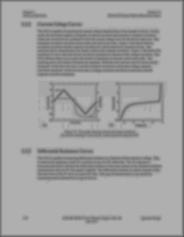


AnalyseaComplex CircuitFailurein
InterlayerCircuit Structures

ADVANCED IMAGING AND DIFFRACTION TOOLS FOR TRANSMISSION ELECTRON MICROSCOPY

Thermographyforthe Analysisof Combustionand ExplosionProcesses


The Drive to Faster Data Transmission

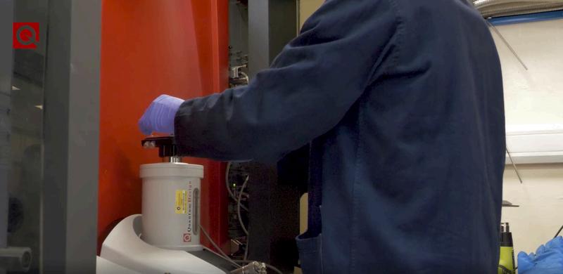
MAGNETIC IMAGING TECHNOLOGY USES QUANTUM DEFECTS IN DIAMOND TO MAP BURIED ELECTRICAL CURRENTS


Fault Isolation on Chips and Power Modules

Electronic failure analysis sits at the intersection of relentless technological progress and the demanding expectations of modern industry and academia. As devices become smaller, faster, and more densely integrated, the challenges associated with identifying root-cause failures grow exponentially. Today’s engineers must contend with multilayer architectures, sub-20 nm defect modes, complex material stacks, and subtle interactions that can compromise performance long before a device reaches the field. Academic researchers face similar hurdles as they push the boundaries of new materials, novel device concepts, and advanced manufacturing processes—often without the analytical frameworks that mature technologies enjoy.
Across both sectors, the need for highresolution, non-destructive, and highly selective measurement techniques has never been greater. Whether troubleshooting intricate circuit behaviour, analysing emerging interfaces, or validating next-generation fabrication methods, success depends on tools and methodologies capable of revealing hidden mechanisms with clarity and confidence. This magazine brings those challenges—and the innovations addressing them—into sharp focus.


Welcome to Electronic Failure Analysis, magazine, brought to you by Quantum DesignUKandIreland.
As device geometries shrink and architectures grow increasingly complex, understanding failure mechanisms has never been more critical. In this edition, we explore cutting-edge methods that push the boundaries of what can be detected, measured,andunderstood.
Our contributors take you inside the challenges of analysing complex circuit failures in advanced interlayer structures and explain how ellipsometry is unlocking new perspectives in materials and interface evaluation. We also highlight techniques for identifying sub-20 nm defects and ultrathin residues issues that can silently compromise semiconductor reliability. Beyond materials analysis, we examine how infrared imaging is enabling truly contactless electronic measurements, offering new insights during development andtroubleshooting.
Finally, a detailed case study shows how STMicroelectronics has successfully implemented the E-LIT solution across two fabrication plants, demonstrating real-world impactatscale
Luke Nicholls
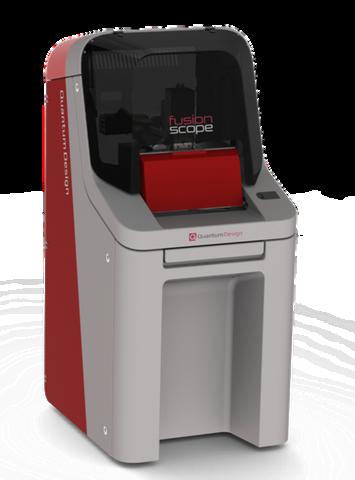
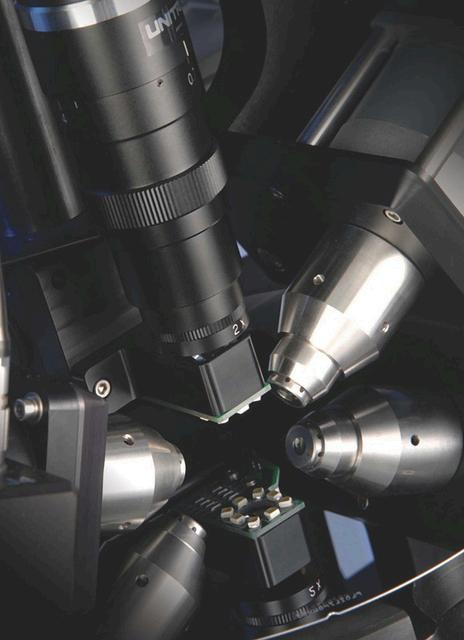
By combining the complementary strengths of SEM and AFM, FusionScope opens the door to a whole world of new application possibilities.
Modes: SEM, AFM Topography, EDS
Sample: Interlayer VIA Circuit

Failure analysis and quality control procedures are very important for determining errors in the manufacturing process and increasing yields of manufactured devices. This can be especially challenging in interlayer circuits, such as a VIA (Vertical Interconnect Access) circuit (Figure 1). In these cases, a three-part analysis using the correlated capabilities of SEM, AFM and EDS in the FusionScope can greatly increase knowledge about samples and help in their improved manufacturing.
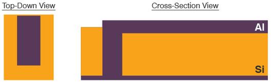
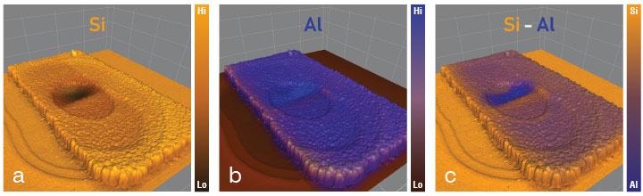
(Figure 1) Top-down and cross-section views of the VIA circuit
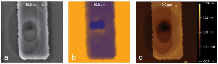
First, the SEM is used to map the large area and identify potential spots of failure by providing detailed imaging of the overlay error that occurs when layers of material are misaligned, decreasing the contact area and potentially lowering the device performance or in some cases leading to failure. The SEM image also provides high-resolution lateral information on the X and Y axes, facilitating the precise measurement of overlay accuracy (Figure 2a).

(Figure 2) SEM (a), EDS X-ray (b), and AFM-Topography (c) images of a failure spot. EDS analysis was able to distinguish the Al line and the Si substrate as well as the position of the Al VIA – the dense, purple-colored region at the upper section of the oval feature (b) Additionally, there are slightly brighter yellow regions (equal to higher concentration) around the VIA, indicating a greater Si concentration This is expected since the Al line is thinner over the VIA (see AFM image) Consistently, a lesser amount of Si signal is detected from the VIA since the top material is Al in this region (b).
FusionScope’s unified coordinate system, along with the coordinates provided by the SEM, allow AFM measurements to be easily gained by executing an automated scan command. The complementary vertical surface information provided by the AFM data reveals the topographic details of the surface along the Z axis, which are not clear in the SEM image. In this example, the AFM reveals that the circuit line is thinned over the VIA, potentially contributing to an impaired electrical connection (Figure 2c)
The SEM (Figure 2a) and AFM (Figure 2c) images show an oval region in the center of the line, which might lead to the conclusion that the VIA covers this entire area, ensuring a proper electrical connection However, the elemental information acquired by the EDS image (Figure 2b) reveals a higher concentration of aluminum (Al) at the upper central part of the oval feature, surrounded by silicon (Si) This indicates that the VIA is not centered and is smaller than the oval feature observed in the SEM and AFM images By combining this with the topographic information from AFM (Figure 3) we can determine that the VIA only contacts the top Al line, where the line is thinned, indicating an even weaker electronic connection.
It would not be possible to fully understand the details of this failure without the correlated information from SEM, AFM, and EDS. This correlative approach allows for more
precise identification and characterisation of defects, improving diagnostic accuracy. This way, the weaknesses in the design and production process can be better identified The ability to analyse failures rapidly and accurately can reduce downtime and costs associated with troubleshooting and repairs, ultimately enhancing the reliability and performance of electronic devices.
(Figure 3) Correlation of 3D topography view with EDS X-ray data. The colors represent the material concentration instead of the height. On the left-hand side (a), only the Si channel is superimposed onto the 3D image; in the middle (b), only the Al channel is superimposed; and on the right-hand side (c), both Si and Al channels are superimposed onto a 3D representation of the AFM topography image. In this way it becomes clear that the Al portion of the VIA is located in a thinned area which most likely leads to poor or faulty performance.


ELLIPSOMETRY EXPLAINED
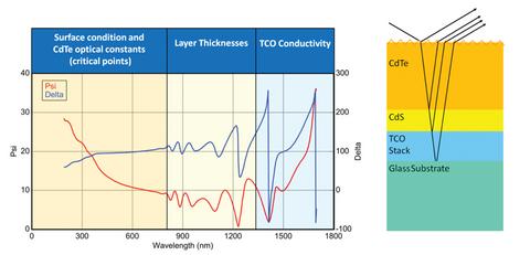
Ellipsometry is an optical technique that probes how polarised light changes when it reflects from (or transmits through) a material, and from those changes it infers properties like thin-film thickness and optical constants (refractive index, extinction coefficient, dielectric function)
That allows failure-analysis engineers to check whether an internal layer failed, degraded, delaminated, or otherwise changed.
Process-control,qualityassurance, anddetectingsubtlemanufacturing defects
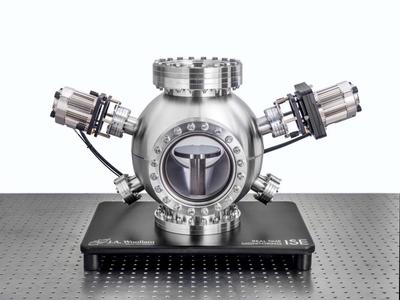
Because ellipsometry can be fast and non-destructive, it can be used for routine inspection, QA, or failure screening to catch defects early in manufacturing or after processing (eg after deposition, oxidation, etching, cleaning, or annealing) That helps avoid larger failures downstream. Woollam’s insitu versions (like iSE) make it possible to monitor layer growth or etch processes in real time, potentially identifying problemsastheyarise
Analysisofburiedinterfacesand detectionofinterfacialissuesin semiconductor/thin-filmdevices
Ellipsometry (especially spectroscopic ellipsometry) can probe aspects such as optical constants and possibly electronic properties at or near interfaces which can be critical when interface degradation, interdiffusion, or contamination leads to device failure. In research contexts, combining ellipsometry with other methods (e.g. photoemission) has been used to reconstruct band diagrams or examine interface quality in non-ideal heterointerfaces
WhyWoollamellipsometersare especiallyusefulinfailureanalysis
Woollam’s instruments stand out because:
Broad spectral coverage Their ellipsometers cover a wide range of wavelengths (from deep UV to IR), enabling analysis of a wide variety of materials and coatings (semiconductors, oxides, metals, organics, etc) This flexibility is helpful when dealing with complex devices made from different materials.
High sensitivity and precision
Ellipsometry from Woollam is sensitive enough to detect very thin films, subtle variations in optical properties, and small changes in surface or film conditions critical for catching early signs of failure or degradation
Non-destructive and fast
Because it does not require destructive cross-sectioning or alteration of the sample (unlike e.g. cross-section SEM, TEM, or physical profilometry), it’s ideal for samples you need to preserve, validate, or returntocustomers/devices.
Adaptability to multilayer stacks and complex structures
Modern electronics often use complex multilayered films. Woollam ellipsometers are designed to handle such
such complexity, and sophisticated modelling (with their software) enables decomposition of multilayers to reveal thickness, refractive index, andmoreforeachlayer
Capability for in-situ or process monitoring With dedicated systems (e.g. iSE), you can monitor deposition, etch, or other processing in real time useful for quality control or diagnosing process-related failuresbeforefulldevicefabrication.
Thin-film passivation layer on a semiconductor degrades or becomes non-uniform, causing leakage
Multilayer dielectric/metal/dielectric stack inside an integrated device shows degraded performance
After a deposition or etch process, layer thickness is out of spec, risking device failure or poor yield
Suspected contamination or oxidation at a buried interface affecting device reliability
Quality assurance or failure screening for large batches of (sensitive) devices without destroying them
Detect changes in film thickness, roughness or refractive index indicating thinning, oxidation or degradation
Non-destructively inspect each layer’s thickness or optical constants to locate faulty or degraded one
Non-destructively inspect each layer’s thickness or optical constants to locate faulty or degraded one
Use spectroscopic ellipsometry (potentially complemented with other methods) to detect changes in optical constants or interface properties
Rapid, non-destructive scans (thickness, uniformity) across many wafers or substrates to detect anomalies
Woollam ellipsometers provide a nondestructive, highly sensitive, and versatile optical metrology solution making them a valuable asset in the toolkit for electronic failure analysis. By enabling precise thin-film measurements, multilayer stack analysis, insitu process monitoring and material-property evaluation, they help engineers catch subtle defects, degradation, or process deviations that could lead to device failure.
TodiscusstheJA Woollamrangeof ellipsometersandyour application,pleasecontact ourTechnicalDirector,Dr. ShayzIkrambyemail,or call(01372)378822
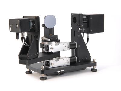
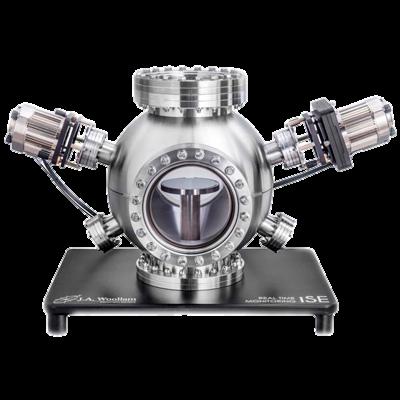
i S E E l l i p s o m e t e r
T h e i S E i s a n i n - s i t u s p e c t r o s c o p i c e l l i p s o m e t e r d e v e l o p e d f o r r e a l - t i m e m o n i t o r i n g o f t h i n f i l m p r o c e s s i n g U s i n g o u r p r o v e n t e c h n o l o g y , t h e i S E
e n a b l e s u s e r s t o o p t i m i s e o p t i c a l p r o p e r t i e s o f
d e p o s i t e d f i l m s , c o n t r o l f i l m g r o w t h w i t h s u ba n g s t r o m s e n s i t i v i t y , a n d m o n i t o r g r o w t h k i n e t i c s
l a n d v e r s a t i l e t o o l N o o t h e r
e l l i p s o m e t e r t e c h n o l o g y a c q u i r e s a f u l l s p e c t r u m f a s t e r
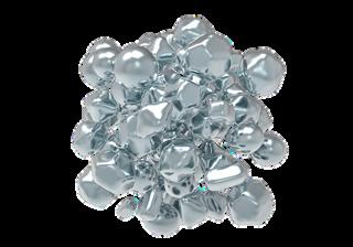
Most people don’t think it is possible to chemically identify molecules at the nanoscale. However, IR PiFM has the sensitivity and spatial resolution required to name the compound of sub–100nm defects and directly visualise monolayers based on their molecular vibrations”


With shrinking semiconductor device sizes and modern advanced packaging processes, it is crucial to eliminate sub-20 nm defects and surface contaminants. To do so effectively, one must be able to discern the molecular identity of a defect/contaminant.
While the presence of defects as small as 20 nm can be detected with survey tools, the traditional suite of analytical tools such as XPS, ToF-SIMS, or SEM/TEM EDX —have difficulty in clearly identifying the contaminating source of defects, especially if they are organic.
Organics are difficult to identify at this scale because traditional analytical tools either lack the spatial resolution required, or they only provide elemental information Infrared photoinduced force microscopy (IR PiFM) can fill this gap by offering the ability to identify or name chemical compounds with nanometer-scale resolution.
It does this by combinging a noncontact AFM with IR spectroscopy to acquire topographical and chemical information concurrently at the nanoscale [1]. Since PiF-IR spectra match FTIR spectra for a given material, existing IR libraries can be used to identify defects analysed with IR PiFM.
Given PiFM’s sub-5 nm spatial resolution, even a multi-component defect can be de-composed into pure components via multivariate data analysis of PiF-IR spectra from different regions of a defect.
In Figure 1, a particle is found (within the red dotted circle) that is about 3 nm in height. The particle appears to be ~20 nm wide laterally. Since the AFM tip isn’t infinitely sharp, the particle is most likely a sphere with a diameter of ~3 nm whose width is dilated by the AFM tip’s radius of curvature which is about ~20 nm. The blue PiF-IR spectrum acquired on the particle matches the orange FTIR spectrum for silica from the Wiley IR library [2].
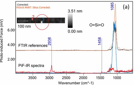
Figure 1 PiF-IR spectrum from a 3 nm particle found on a silicon surface is identified to be a silica particle by searching the Wiley KnowItAll IR library
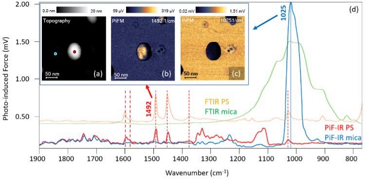
Another good example of how PiF-IR spectroscopy and PiFM imaging can be used to directly name materials at the nanoscale is shown in Figure 2. This sample is a 20 nm polystyrene (PS) particle deposited onto a mica surface. The inset shows the AFM topography and the PiFM images. PiFM images are essentially chemical absorption maps which show how strongly the material absorbs light of a given wavenumber, in this case 1492 cm 1 that highlights the PS particle and at 1025 cm 1 which highlights the mica surface. The lateral size is again dilated in the topography by the tip’s radius of curvature, so again, the height is going to be the best measurement of the diameter of the particle.
The red PiF-IR spectrum acquired on the nanoparticle and the blue spectrum on the surface match the FTIR spectra for PS (orange) and mica (green) well. For PS, all the prominent FTIR peaks are clearly visible in the PiF-IR spectrum acquired on the particle.
Figure 2 AFM topography, PiFM images, and PiF-IR spectra acquired on a 20 nm polystyrene nanoparticle.
The additional peaks on the particle (between 1100 and 1350 cm 1) may be due to the presence of a surfactant layer used to disperse the nanoparticles.
Besides particulate defects, surface contamination can be another large issue in semiconductor processes Dirty surfaces can interfere with bonding processes in modern advanced packaging processes. With monolayers, it is difficult to even detect its existence, let alone identify it. Many people currently rely on making inferences about the surface of a sample based on unreliable information like water contact angle measurements. However, PiF-IR spectra and PiFM images can detect and characterise monolayers directly.
In Figure 3a, five PiF-IR spectra acquired on an otherwise clean wafer from a storage container are shown at the bottom of the figure The fact that they are quite repeatable even though they are acquired from 5 different locations suggests a homogeneous surface chemistry. In addition to the silicon oxide peak at 1130 cm 1, they show a strong peak at ~ 1250 cm 1. When these spectra are averaged (blue spectrum) and a search performed in the Wiley IR library, one finds it matches the FTIR spectrum of perfluoro polyether (PFPE) which is shown in orange Given the ultra-flat topography, the PFPE is expected to be a conformal monolayer that covers the surface quite uniformly
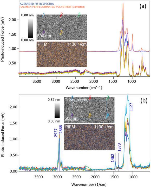
Note that even though the surfaces in Figure 3a and 3b are contaminated with different molecules, the microroughness of the silicon substrate remains the same, showing how thin the contaminant layers must be. Also, the PiFM image at 1130 cm 1, which highlights the silicon oxide, shows much more contrast variations across the surface after the plasma cleaning as compared to the original one.
This is consistent with the varying peak strengths observed in the spectra, suggestive of subtle differences in the oxide at different locations. This shows how useful nanoscale IR measurements are for looking at surface preparations. Without PiF-IR spectra, it would be impossible to know about surface contaminants like these, let alone track down where they might be coming from.
As another example, the cleanliness of copper surfaces as they are prepared for hybrid bonding can be examined. Hybrid bonding is gaining interest as replacement of thermal compression bonding for advanced packaging applications that require higher interconnect density. An important element to ensure successful hybrid bonding is an extremely flat, smooth, clean, and hydrophilic dielectric surface that is properly terminated with Si-OH bonds that can bond together instantaneously upon contact at 25 °C.
Additionally, to form good metal-tometal bonds, the Cu surfaces must be free of organic contaminants and carbides which prevent true Cu interfacial grain growth. It is known that benzotriazole (BTA), which is used as an inhibitor to protect recessed copper, reacts with copper ions to form a thin Cu(II)-BTA polymer on the copper surface that is difficult to remove [3].
Figure 4 shows averaged PiF-IR spectra of four copper surfaces: (a) as electroplated, (b) after the electroplated copper is treated by BTA, (c) after CMP process pf electroplated copper, and (d) after Ar ion cleaning following the CMP process. The as-electroplated copper (Figure 4a) shows a peak at around 730 cm 1, which can be attributed to copper oxide. When the copper is treated with BTA (Figure 4b), two peaks at ~795 and 755 cm 1 appear. These peaks are attributed to the C-H stretching vibration of the benzene ring in BTA, clearly indicating the formation of Cu-BTA polymer [3]. These two peaks are also present in the copper sample that undergoes a CMP process (Figure 3c) even though the peak at 795 cm 1 appears as a shoulder of a new peak
The prominent new peak at ~615 cm 1 is typically associated with Cu2O4. When the same sample is cleaned via Ar ion beam (Figure 4d), the copper surface is mostly clean, except for a small peak at ~805 cm 1, which may be due to the oxide peak associated with the AFM tip. Lastly, note the sharp feature at ~905 cm 1 in all spectra is an artifact of laser power normalisation, so it can be safely ignored.
Even though other surface sensitive techniques such as XPS can be used to check for the presence of the CuBTA complex, the advantage that PiFM offers is that its spatial resolution allows examination of individual copper pads, which are getting smaller than 1 µm in size. OFFERING THE HIGHEST RESOLUTION NANOSCALE CHEMICAL ANALYSIS INSTRUMENTS AVAILABLE.
.
IR PiFM can chemically identify sub20 nm defects, regardless of whether they are organic or inorganic materials. It can also detect and characterise monolayer residues efficiently, without contaminating the sample This is a huge advantage compared to something like SEM analysis which typically contaminates samples with carbon deposits.
IR PiFM also can be used to check post-CMP residues sensitively even on individual copper pads for Cu-Cu hybrid bonding applications; IR PiFM’s capability to evaluate the density of Si-OH bonds on SiO2 surfaces after cleaning processes is covered in a separate application note. IR PiFM is available on instruments which support up to 12” wafers with many automation features, including automated defect analysis based on KLARF coordinates.
Contact Dr. Shayz Ikram to discuss your defect and residue analysis needs and for a demo on your own samples.
Call (01372) 378822 or Email: shayz@qd-uki.co.uk

Existence of IR PiFM for AFM plus IR spectroscopy/mapping with sub–5-nm spatial resolution
Understand the applications of IR PiFM in semiconductor metrology
Review application examples in naming sub–100-nm particulate defects and ultrathin conformal surface contaminants
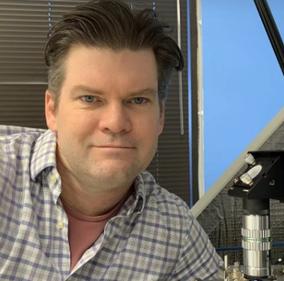
Speaker: Derek Nowak, PhD VP, Technical Operations
Molecular Vista
Researchers in failure-analysis labs in semiconductor-related companies
Users of KLA’s Surfscan and other defect-finding instruments
Advanced packaging (coppercopper hybrid bonding) process engineers
EUV and other advanced lithographic process engineers
WATCH THE WEBINAR HERE

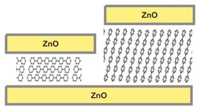
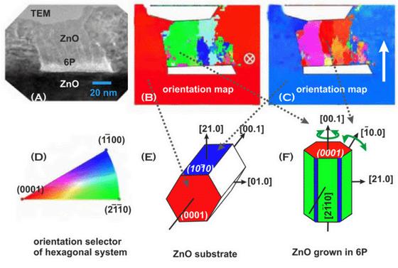
Faster chip performances in ever shrinking electronic devices push circuits down to nanometer size. Spintronic devices and optical properties of organic semiconductors depend on their nm level local structure . Orientation and phase mapping with ASTAR sheds light to local texture and phases, while 3D electron diffraction tomography reveals detailed crystal structure of possible impurities. As metrology tool detailed strain maps down to nm scale allow to monitor precisely electrical properties and avoid device failure.


For this reason, ASTAR was used to uncoveranyspecificsoftheovergrowth regimeofZnOon6Patnmscale.

WithASTARscanningtheelectronbeam in nanobeam diffraction mode (probe diameter 1 nm) across an area of 100 nm in width and 80 nm in height providestheorientationmapsdepicted below. The maps were derived by comparing the diffraction pattern recorded at each position with a set of about 1000 calculated diffraction patterns of hexagonal ZnO. Focussing on ZnO atop 6P, columnar grains are identified that extend even up to the surface as signified by green and red areas
From the ASTAR orientation map it is evident that the [00.1] wurzite axis is well-aligned along the vertical growth direction indicating a strong texture Electrostatic forces originating from the 6P molecules have to be considered as the origin of this texture. In addition, a significant lateral texture within the (0001) plane cannot be excluded, as it cannotbedistinguishedwhichofthesix prismatic facets contribute to the diffractionpattern.
Experimental Data:
TEM Type: JEOL 2200 FS
Map resolution: 1 nm
Scanned area: 100 x 80 nm
Crystal Structure:
ZnO: Hexagonal, P6₃/mmc
a= 3.22 Å
c = 5.20 Å
Research on ZnO is of immediate practical importance as this semiconductor has several favourable properties, including good transparency, high electron mobility, wide bandgap, and strong roomtemperature luminescence. These properties are used in emerging applications for transparent electrodes in liquid crystal displays, in energysavingorheat-protectingwindows,and in electronics as thin-film transistors andlight-emittingdiodes(LEDs).
Fig. 1) Crystallographic orientation mapping of ZnO as revealed by scanning nanobeam diffraction (SNBD):
a) TEM image of the region analysed by SNBD. b) and c)
crystallographic orientation maps of ZnO. The white arrow markers represent the lattice planes colour coded by the orientation triangle of d)
e) alignment of a representative ZnO unit of both, ZnO substrate and low temperature grown homoepitaxial ZnO, f) alignment of a representative ZnO unit for the textured growth atop sexiphenyl
Based on Precession Electron Diffraction (PED), NanoMEGAS offers several automated and robust unique applications A hardware (DigiSTAR P2010) to control specifically the coils of any TEM, is a scan and precession generator simultaneously, that is used either for static acquisition of ED, or scanning ED, suitable also for precession enhanced 4D-STEM (named 4D-SPED).
LEARN MORE

Get in touch

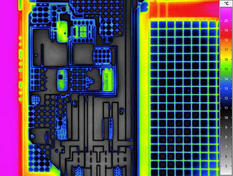
The thermographic inspection of electronic components and assemblies is an established test procedure for failure detection and quality management – from the development of first prototypes to serial production.
This enables, for example, the following to be detected:
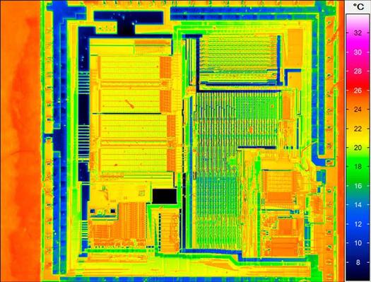
Hotspots and atypical temperature distributions on the surface of printed circuit boards, integrated circuits and multichip modules
Increased contact resistances
Increased resistance due to constriction of wires
Hidden cracks in joints
Power losses due to RF mismatch
Incorrect thermal connections of heat sinks
Short circuits, soldering defects such as cold solder joints

Thermographic analysis during each development step provides important conclusions for the optimisation of heat management and the design of complex electronic assemblies. In electronics production thermographic temperature measurement is used as a versatile instrument for quality assurance. Highperformance thermography has become indispensable for setting critical technological parameters and their permanent monitoring as well as for inline testing of products in the production process and their final functional test.
Influences neither the RF impedance of the measurement object nor the heat dissipation of the same, which serves the safe avoidance of corresponding measurement errors
Allows safe temperature measurement even on live working parts
Complete recording of the temperature distribution and its temporal course of complex assemblies
Highest spatial resolution by using measurement systems with detectors with a very high number of pixels and opto-mechanical MicroScan unit
Resolution of smallest geometrical structures using close up lenses and infrared microscope lenses
Detection of smallest temperature differences using cooled photon detectors and lock-in measurement methods
Easy-to-use analysis and documentation of measurement results with powerful analysis software
Detector resolutions up to (1,920 × 1,536) native IR pixels for testing complex assemblies
Capturing of high-resolution detail images with pixel sizes up to < 1 μm using specific microscopic lenses
Detection of temperature differences between defective and intact structures in the range of a few micro-Kelvin due to high thermal resolution up to < 0.015 K in combination with the lock-in method
Measurement accuracy of up to ± 1 °C or 1 % for accurate measurement results
DISCOVER
“ TodiscusstheInfraTecrangeof thermographiccameras,getin touchwithDr LukeNichollsby emailorcall(01372)378822
high-end infrared cameras have a high number of pixels, which are crucial for the recognition of details. The analysis of complex assemblies and individual components requires technology with high geometric and thermal resolution. Anyone who examines assemblies where defects cannot be localised with conventional functional tests can create comparative images of fault-free assemblies. Comparative analysis of the thermograms is then often sufficient to identify the fault. Thus, errors can be detected and eliminated in a time-efficient and simple manner.“
Marian Kerze Development Infrared Cameras InfraTec

The principle of non-contact thermographic temperature measurement allows the error-free determination of the temperature of small objects with small heat capacity. This is often impossible, however, even when using the smallest contacting temperature sensors, as their heat dissipation frequently falsifies the measurement results In many cases, the use of thermocouples is impossible due to the design or function of the circuit itself. In addition, the structures of electronic measurement objects are sometimes so small that temperature sensors cannot be attached to them.
However, thermographic systems with a high spatial resolution are able to make such small structures clearly visible and, in addition, to determine their exact temperature distribution along with their chronological sequence By means of specific close-ups and powerful infrared microscopic lenses, users can thermographically measure hotspots of just a few micrometres in size on the surface of components such as semiconductor components.
If SIL lenses (Solid Immersion Lenses) are additionally used, even smaller structure sizes can be detected In combination with appropriate active thermography methods (lock-in thermography), temperature differences of less than 1 mK are clearly visible for failure localisation.
InfraTec offers matching lenses and cameras with cooled and uncooled detectors with native resolutions up to (1,920 × 1,536) IR pixels. With MicroScan –available for cameras with both cooled and uncooled detectors – the spatial resolution can be further improved
By means of lock-in analysis procedure of InfraTec’s IRBIS® 3 active, errors that only cause mK or μK deviations can be reliably detected and assigned to their location: The thermograms obtained in this way ensure that components and assemblies are depicted down to the smallest detail and that failures can be precisely detected and localised. Thermal images with an enormous spatial resolution of a few megapixels pay off especially for complex assemblies, where many structures can be captured simultaneously on the respective measurement and test object If the pixel number of the detector of the used camera is too small, the number of images required for the complete acquisition of the measurement object increases.


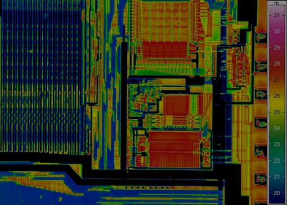
C A S E S T U D Y
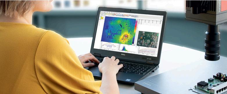
STMicroelectronics is a European manufacturer of semiconductor devices and integrated circuits with locations worldwide. Their products are mainly used in the automotive industry and for the Internet of Things (IoT). The company performs nondestructive failure analysis of chips, discrete components, sensors, LEDs and power modules using InfraTec's E-LIT system in Shenzhen (China) and Calamba (Philippines).
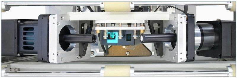
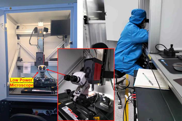
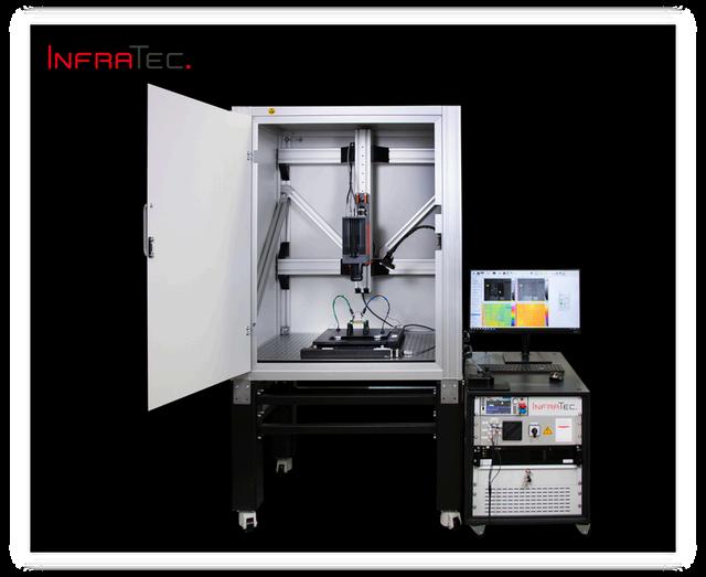
The E-LIT solution employs lock-in thermography, a method, in which local defects are detected and analysed based on thermal anomalies generated by defined electrical excitation of an electronic component or assembly. At STMicroelectronics, the test system –
comprising an excitation source, an infrared camera with adjustable Z-axis positioning and various lenses, an X-Y table, and additional accessories – was integrated into the failure analysis laboratory. The E-LIT system was further enhanced with a binocular to enable the connection of power supply contacts to the tested components.
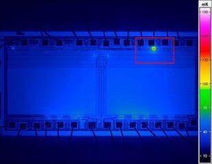
During electrical activation of components under investigation, changes in surface temperature are measured using a high-end infrared camera from the ImageIR® series to identify so-called "hot spots”. This allows even the smallest defects, such as point and line short circuits, oxidation, and faults in transistors and diodes within circuits, which cause only minimal temperature deviations in the millikelvin (mK) or microkelvin (μK) range, to be detected

For the analysis of large components, the E-LIT system is equipped with 25 mm lenses that provide a wide field of view, along with several microscope lenses capable of resolving fine details up to 1,3 µm. Hot spots can be detected with high sensitivity at chip level using as little as 2 μA. To excite power modules, high voltages up to 3 kV are applied The analysis is performed using InfraTec’s IRBIS® 3 active online operating software, which offers a wide range of comprehensive analysis functions. The use of various colour palettes, including inverted and weighted modes, has proven particularly effective for fault detection. By sharing their practical experience, users help InfraTec continuously enhance the E-LIT system for new test objects and faster results and in return, they promptly benefit from updates and advancements.
Lock-in thermography is a key method at STMicroelectronics for identifying faults in electrical components The user friendly method is especially effective in exactly locating short circuits and other anomalies.
Users particularly appreciate the simple visual identification of faults and the flexibility of the system for measurements on different components such as ICs, sensors, LEDs or power modules. The ELIT solution played a crucial role in the approval of a new mass production project in Calamba, where it was used to quickly pinpoint hot spot locations across multiple batches


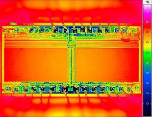
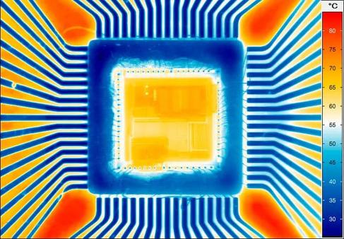
Infraredimageofamicrochip
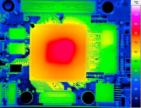
Thermographyimageofaprocessor

Hot-spotdetectionofGaN-HEMTS
Infraredimageofanelectronicboard
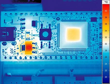
Lifetimeanalysisbytemperaturemeasurementofa voltageconverteronamicrocontrollerboard
Structuresonamicrochipat8xmagnification


Find out in this white paper how you can use lock-in thermography to detect faults in electronic and semiconductor components. Benefit from practical tips and achieve the best possible measurement results with the E-LIT test bench from InfraTec.
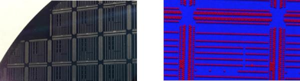
discover hyperspectral imaging cameras

Hyperspectral imaging enables precise analysis of surface uniformity, layer thickness, and defect detection. In semiconductor manufacturing, even the slightest inconsistencies in wafer coatings or material composition can lead to failures in electronic components Hyperspectral imaging allows the assessment of thin-film deposition, contamination, and microstructural variations withoutdamagingthewafer.


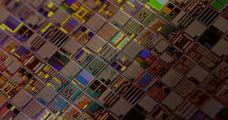
Electronic components are everywhere in our modern world. These components must be reliable, as they control critical systems from everyday items to electronically controlled military equipment and various aerospace equipment.
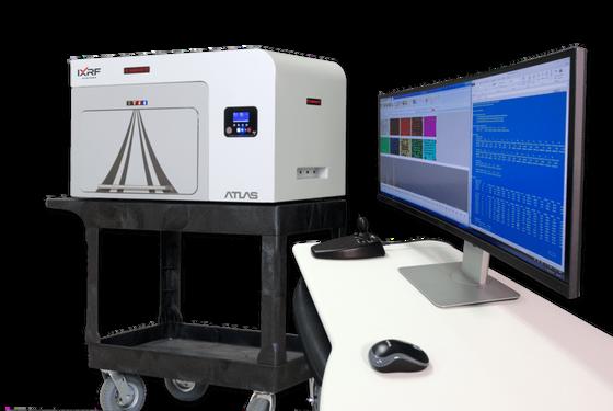
To assure this reliability, components must go through a battery of tests XRF analysis is an irreplaceable tool for the semiconductor industry to guarantee and certify their products
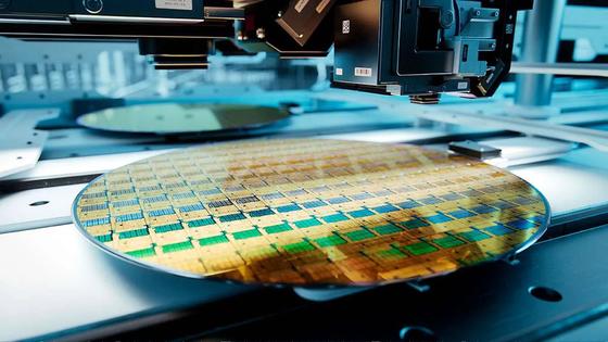
Electrical or photonic circuits are one of these components that are the foundation for so many other products. These circuits begin their lives on silicon wafers As the wafers and associated circuits and boards become more specialised, they require different types of testing.
IXRF Systems offers a 5µm spot size, the smallest on the market, allowing for extremely high resolution maps, analysis of small leads or pillars. Though SnPb solder has its place in technology, there is now a shift to use SnAg due to environmental, health and safety concerns. These solder points must also be tested.

Current technologies include Pb-free bumps of SnAg, as well as Pb-free SnAg pillars on Cu seed Current bump/pillar and seed sizes are about 50 to 150µm However, next-generation technology is pushing towards smaller pillar/seed sizes of 20- 30µm.
Leads on electronic components cannot fail, less the whole system will fail. A wellknown phenomenon known as ‘whiskers’ can cause these components to fail. The whiskers come from tin used in electronic component surfaces.
It has been found that adding lead to the tin can prevent the growth of whiskers. This addition of lead must be analytically measured to ensure expected and required concentrations Most aerospace companies require a minimum of 3% Pb to prevent tin whiskers.
XRF is the preferred method for lead testing in tin XRF is more accurate than EDS based on the larger area and depth of measurement
IXRF Systems’ powerful software can quickly identify, measure, and analyse multiple solder bumps on a board.
Quantitative analysis was done on one of the SnPb solder bumps in the centre trio section, a circled portion in the elemental map (fig. 2).
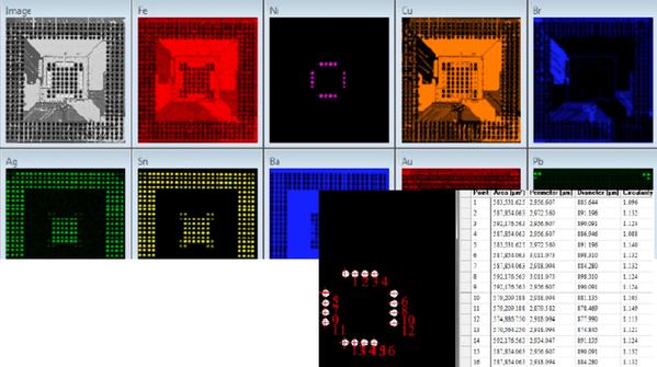
IXRF Systems’ ATLAS SEMI can analyse for:
Bump inspection
CMOS image sensors (CIS)
Corrosion resistance coating
Cu CMP control at BEOL
Film stack
Light elements
Metal film stack composition such as CIGS
Multi-stack structures
Pb measurement for Whiskers
Redistribution layer (RDL)
Sn/Ag Bump/Pillar measurements

Sputtering targets
Thermal barrier coating
Thick mono-layers
Thickness and composition control
Thin Film/Coating thickness measurements
Ultra-thin films
Under bump metallisation (UBM)
Wafer-level packaging (WLP)


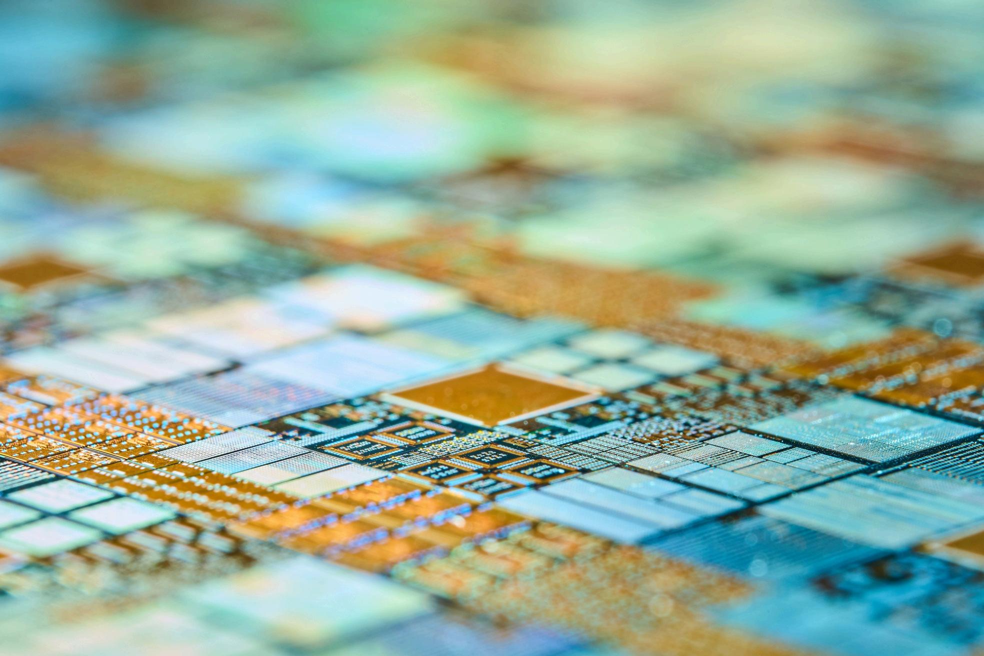
In semiconductor and microelectronic devices, failure can be caused by:
Local current leakage
Short circuits or open circuits
Electromigration
ESD (electrostatic discharge) damage
Hot spots or current crowding
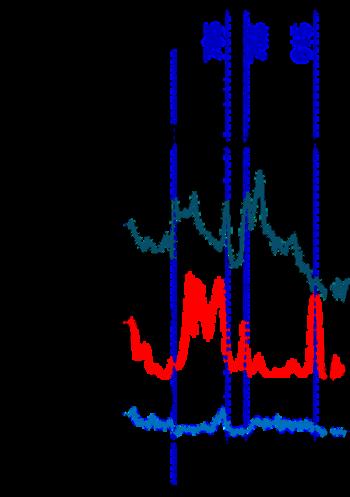
Traditional EFA methods — such as Emission Microscopy (EMMI), Magnetic Force Microscopy (MFM), Lock-in Thermography (LIT), and SQUID microscopy — each have tradeoffs in sensitivity, spatial resolution, and non-invasiveness.
QDM provides a powerful alternative...
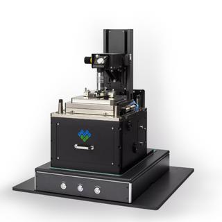
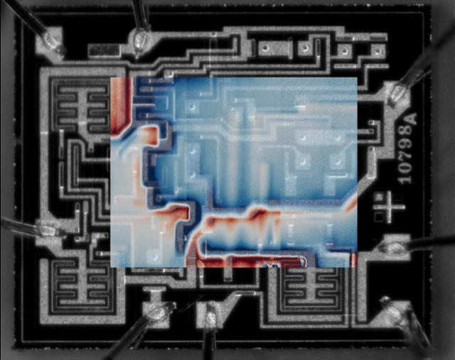
EuQlid's magnetic imaging technology uses quantum defects in diamond to map buried electrical currents
The quantum diamond microscope offers wide-field imaging of magnetic fields with highest sensitivity. It uses a nitrogen-doped diamond chip to simultaneously image the magnetic fields of a sample over a large area The user-friendly benchtop system can measure both, the strength and orientation of the local field in real time
The Quantum Diamond Microscope is the first system to combine the sensitivity of NV-center based measurement technology with a widefield microscope
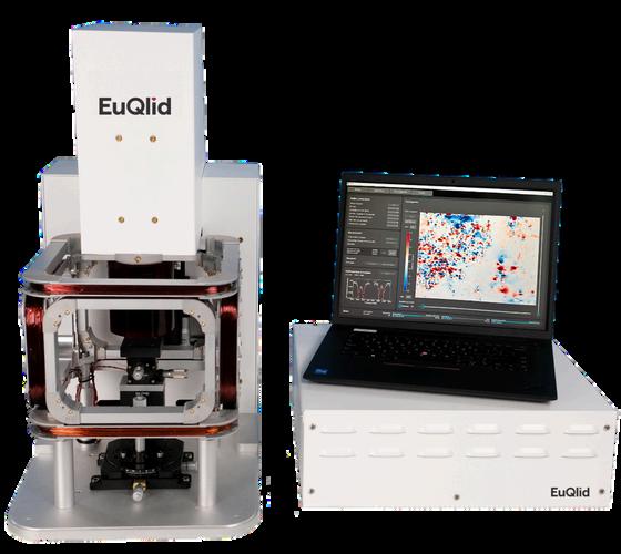
DISCOVERTHEQDM
EuQlid's Qu-MRI uses Quantum NVdiamond magnetometry to deliver buried electrical current maps.
Next-generation semiconductors require 3D architectures to deliver improved performance, cost and power EuQlid's magnetic imaging solution addresses a foundational need for non-invasive identification of buried connectivity defects during design and high volume manufacturing
Image millitesla to nanotesla magnetic fields: Tunable spatial resolution down to less than one micron and field-of-view up to four millimeters in a single image Larger samples can be readily mapped bytiling multiple images
Correlate Magnetic and Optical Images: Collect magnetic and optical images of samples using the same optical system for straightforward co-registration
Vector Measurements: The diamond sensor enables reconstruction ofthe magnitude and direction of magnetic fields, providing superior reconstruction of magnetic source distributions
Quantum-Grade Diamond: Manufactured by EuQlid partner Element Six, with properties optimised for microscale magnetic field mapping applications
Robust and Easyto Use: Operates with no cryogenics, vacuum systems, special infrastructure, or power requirements
Backside Power Delivery and other 3D architecture innovations pose novel challenges for metrology. EuQlid's solution enables spatial analysis of state-dependent power flows in functioning devices to accelerate the validation of new processes and designs
Improving battery lifetime, safety and performance requires understanding exactly how and where degradation initiates and propagates Magnetic imaging enables visualisation of the spatial and temporal current heterogeneities key to mitigating degradation.
EuQlid's technology provides customers with powerful insights, from spatial analysis of state-dependent power flows in functioning CPUs and GPUs, to the detection and localisation of interconnect stacking errors in HBMs.
MJ Turner, N Langellier, R Bainbridge, D Walters, S Meesala, TM Babinec, P Kehayias, A Yacoby, E Hu, M Lončar, RL Walsworth, and EV Levine
Physical Review Applied 14, 014097 (2020).
DOI: https://doi org/10 1103/PhysRevApplied 14 014097
Abstract

Current density distributions in active integrated circuits result in patterns of magnetic fields that contain structural and functional information about the integrated circuit Magnetic fields pass through standard materials used by the semiconductor industry and provide a powerful means to fingerprint integratedcircuit activity for security and failure analysis applications. Here, we demonstrate high spatial resolution, wide field-of-view, vector magnetic field imaging of static magnetic field emanations from an integrated circuit in different active states using a quantum diamond microscope (QDM) The QDM employs a dense layer of fluorescent nitrogen-vacancy (N-��) quantum defects near the surface of a transparent diamond substrate placed on the integrated circuit to image magnetic fields. We show that QDM imaging achieves a resolution of approximately 10 ��m simultaneously for all three vector magnetic field components over the 3 7 ×3 7 mm2 field of view of the diamond We study activity arising from spatially dependent current flow in both intact and decapsulated field-programmable gate arrays, and find that QDM images can determine preprogrammed integrated-circuit active states with high fidelity using machine learning classification methods.

At Quantum Design UK and Ireland, we’re passionate about providing high-tech scientific instrumentation to researchers, universities, and industries across the UK and Ireland
Based in Leatherhead, Surrey, we’re a small but dedicated team, bringing deep expertise and a personal touch to everything we do.
We specialise in materials characterisation, cryogenics, non-destructive testing, imaging cameras, microscopy, and spectroscopy But more than just supplying instruments, we work closely with our customers to understand their unique research challenges and help them find the best solutions.
What sets us apart? We’re knowledgeable, approachable, and always happy to help. Our Sales and Service departments are second-tonone, offering expert support, training, and advice to make sure our customers get the most out of their equipment.
At Quantum Design UK and Ireland, we take pride in being more than just a supplier we’re a trusted partner in scientific discovery.”
For more than 40 years Quantum Design (QD) has been providing technology solutions to researchers in the fields of physics, chemistry, biotechnology, materials science, and nanotechnology.
Established in 1982 in San Diego, California, Quantum Design is the leading commercial source for automated materials characterisation systems offering a variety of measurement capabilities.
Dr. Luke Nicholls Acting Managing Director Quantum Design UK and Ireland

Quantum Design instruments are cited in, and provide the data for, more scientific publications than any other instrument in the fields of magnetics and materials characterisation.
An essential part of providing scientific solutions to researchers around the globe is to also offer state-of-the-art instruments from other leading manufacturers.
QD instruments are found in the world’s leading research institutions and have become the reference standard for a variety of magnetic and physical property measurements

These manufacturers are chosen by QD not only for their innovative products, but also because they believe in the same level of customer satisfaction and support that scientists have come to expect from QD products worldwide.