
Influence of Thickness on Electrical and Structural Properties of Zinc Oxide (ZnO) Thin Films Prepared by RF Sputtering Technique
1M.Momoh, 2S.Abdullahi, 3A.U MorehAbstract: Zinc Oxide (ZnO) thin films were prepared on corning (7059) glass substrates at a thickness of 75.5 and 130.5nm by RF sputtering technique. The deposition was carried out at room temperature after which the samples were annealed in open air at 1500C. The electrical and structural properties of these films were studied. The electrical properties of the films were monitored by four-point probe method while the structural properties were studied by X-ray diffraction (XRD). It was found that the electrical resistance of the films decreases with increase in the thickness of the films. The XRD analysis of the films showed that the films have a peak located at - with hkl (002). Other parameters calculated include the stress ( s) and the grain size (D).
Keywords: Electrical Properties, Film thickness, Structural properties, Zinc oxide.
I. INTRODUCTION
Transparent conducting oxides (TCOs) have a range of highly useful applications as transparent electrodes in optoelectronic devices such as solar cells and flat panel displays. TCO coatings are essential for solar cell applications since they constitute a fundamental part in the emerging new generations of photovoltaic devices. The properties of TCO films include large band gap (>3 eV), low resistivity (103 - 10-4 Ω cm) and a very good optical transmittance (80 - 90%) in the visible range [1]. Though indium tin oxide (ITO) film is extensively applied to photovoltaic devices and flat panel display because of its good electrical and optical properties, it has some problems such as high cost, low stability to H2 plasma and toxicity. Recently, Zinc Oxide (ZnO) thin films have attracted much attention as a transparent and conductive film material because it exhibits a wide band gap, high transparency and low resistivity. As a wide and direct band gap semiconductor material, ZnO has a band gap of 3.37 eV at room temperature, which makes it have potential in blue and ultraviolet (UV) photoelectric applications, such as transparent high power electronics, UV detectors, and short wavelength devices. Its large excitons binding energy of about 60 MeV makes it a good choice for fabrication of excitonsrelated devices, such as short-wave light emitters. Zinc oxide has some advantages over GaN such as higher radiation hardness, simplified processing due to amenability to conventional chemical wet etching and the availability of large area substrates at relatively low material costs, non-toxicity and relatively low deposition temperature [2]. Zinc oxide thin films have been prepared by various deposition methods such as thermal oxidation [3], Spin coating [4] vacuum evaporation [5], electron beam evaporation [6], sputtering [7] - [10] Spray pyrolysis [11] - [14] and chemical bath deposition [15].
In this paper, we report the influence of film thickness on electrical and structural properties of Zinc Oxide thin film grown by RF sputtering technique. This technique is chosen because it provides a higher degree of ionization/dissociation that leads to greater oxidation rate at the substrate surface [16]. In general, the advantages of sputtering are the simple apparatus, high deposition rate, low substrate temperature, good surface flatness, transparency and dense layer formation [17].
II. EXPERIMENTAL
A. Substrate preparation:
Before the deposition, the substrates were kept in a dilute chemical detergent (a detergent solution used in the laboratory to solubilise biological macromolecules such as proteins) solution at 100°C in ultrasonic bath for 10 minutes to remove oils and protein molecules and rinsed with double distilled water to remove possible left detergent contaminants. To remove organic contaminants, the substrates were boiled in dilute hydrogen peroxide- (H2O2) solution for 15 minutes. The substrates were extracted from the bath and rinsed with distilled water and later dried with nitrogen gas before being introduced into the sputtering chamber. Throughout the period of substrate preparation, film deposition and film characterization, the laboratory staff wore protective clothing so as not to contaminate the samples.
B. Thin film deposition:
Zinc Oxide thin films were deposited onto corning glass (7059) substrate using an RF power of 60W. A Zinc Oxide target with 4N purity and 4cm in diameter was located on the cathode, which was about 7cm from the substrate mounting plate. The deposition was carried out at room temperature. Prior to deposition, the chamber was evacuated to 4.6×10⁻³mbar.For plasma formation, research grade argon with 4N purity was used at a pressure range of 10-2-10-1 mbar, oxygen was also added to facilitate the formation of ZnO on the substrate. Other deposition parameters that were kept constant include the deposition temperature, oxygen/argon flow rate and the sputtering RF power. The details of the deposition parameters are shown on table1. In this study, the deposition rate is nearly constant as the sputtering time ranges from 60 to 103.5 minutes. A deposition rate of 1.26nm/minute was therefore obtained.
TABLE I: DEPOSITION PARAMETERS USED IN THE STUDY
The grown films were subjected to electrical characterization by the use of a 4-point probe. Four-point probe method is an electrical resistance measuring technique that uses separate pairs of current-carrying and voltage-sensing electrodes to make more accurate measurements than traditional two-terminal (2T) sensing. A probe head with tungsten carbide tips with a point radius of 0.002", a probe spacing of 0.05" and a probe pressure of 70 to 180 grams was used for all measurements. Current was supplied by a Crytronics model 120 current source with a range of applied currents between 1μA to 100 mA. Voltages were measured by a Keithley model 181-nanovolt electrometer with an input impedance of greater than 1 GΩ. Sheet resistance (Rs in units of Ω/sq.) and resistivity (ρ in units of Ω cm) were determined from;
r= 2ps v I
Where S is the spacing between the probes The crystal structure of the films on the other hand was inspected using PANALYTICAL XPERT PRO diffractometer performed in 2 at a voltage of 45KV and a current of 40mA.The sweeping angle was 20 to 80 degrees, the scan speed 0.8 degrees/minute at a scan step of 0.02 and employing a radiation. The surface morphology of the films was studied by the use of Veeco Dektak 150 profilemeter while the microstructure was determined by EV®MA-10 scanning electron microscope at an accelerating potential of 18kv.The chamber is pumped down to a vacuum range of 10-5 to 10-6 torr. Lattice parameters were then calculated from;
Where h, k and l are the Miller indices, a and c are lattice parameters
III. RESULTS AND DISCUSSION
A. Electrical properties:
Table II shows the resistivity and sheet resistance of the films annealed in open air .It can be seen that the resistivity for the 75.5nm thick film is greater than that of the 130.5nm film. It is known that ZnO thin films generally exhibit n type conductivity, its value depending on the deposition parameters. This conductivity has been attributed to intrinsic donor defects such as donor vacancies and Zn interstitials. More recent reports have proposed that the conductivity is due to hydrogen, since hydrogen impurities can interact with oxygen vacancies resulting in complexes that can act as shallow donors. In any case, experimental conditions such as substrate temperature and deposition time (directly related to the film thickness) can influence the intrinsic defect concentration, thus affecting the conductivity of the films. The observed increase in the conductivity can be correlated with the decreased concentration of grain boundaries in thicker films due to the presence of bigger grains and improved crystallinity, which can reduce scattering processes and increase the conductivity. In addition, the increasing of the thickness can lead to higher concentration of intrinsic defects and thus to an increased conductivity [18]. According to [19] the decrease seen for the sample was as a result of increase in carrier concentration and mobility. Furthermore, the increase in carrier concentration could be attributed to crystallization of the grains into a dense structure in the film [13]. There are two reasons for the increase in carrier concentration. First, many free electrons are caught by large numbers of traps formed by defects. Second, when a semiconductor is abruptly terminated at the surface, the disruption of potential function would create discrete energy states within the band gap which were called surface states and could trap free carriers. [20], further explained that the increase of conductivity in the 130nm thin film may be due to the increase in inter metallic island distance with the increase of film thickness.
In a research, [1], concluded that with increase in the thickness of the thin films, carrier mobility and concentration is also improved which is attributed to the improved crystallinity and increased crystallite sizes that weakens inter-crystallite boundary scattering and increases carrier lifetime. The observed increase in sheet resistance for the 75.5nm film is probably due to the discontinuous nature of the film. The observed dependence of sheet resistance on thickness is in good agreement with Fuchs-Sondheimer theory [21].
B. Structural Properties:
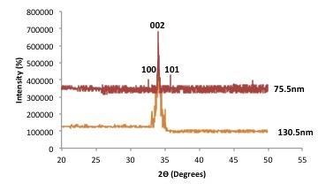
Fig. 2, shows the X-ray diffraction profiles of ZnO films in the thickness of 75.5nm and 130.5nm respectively. From the XRD profile, the film deposited at a thickness of 75.5nm exhibited the (002) orientation at 2=34.310 and 130nm thick 34.350 . The predomination of (002) peak in the pattern proved that the ZnO films have Wurtzite crystalline structure with a preferential orientation along the c-axis and without formation of any secondary phases. The shift of the (002) peak towards higher angles also implies relaxation of the residual strain introduced in the films during the deposition process. The indication that the grains are strongly oriented along the c-axis is because of the singular peak (002 at 2Ɵ ~ 34.31°34.35°). This is in line with the findings of other researchers such as [8]. A qualitative idea proposed by [22] for the formation mechanism of the preferential oriented thin films suggests that it could be the minimization of the surface energy of each crystal plane and usually films grows so as to minimize the surface energy. Due to the minimization of the surface energy, heterogeneous nucleation readily happens at the interface of film and the substrate.
The unit cell (lattice) parameters a and c of the films with (002) orientation were calculated using the relation in equation 2.The values calculated for a and c are 3.03A0 and 5.25 for the 75.5nm thick film and a = 3.2A0 while C = 5.19A0, for the 130nm thick film respectively in agreement with lattice constants of ZnO powder sample of ASTM card: a = 3.2648A0 and C = 5.2194A0. It has been noted that point defects such as Zn antisites, oxygen vacancies and extended defects such as threading dislocation changes the lattice constant [17]. The 75.5nm thick film is noted to have the maximum deviation from the ideal value.
TABLE
A. Morphological properties:
The surface topography of thin film is very important tool to investigate the microstructure of the films. Scanning Electron Microscopy (SEM) micrograph of the two samples is shown in fig. 3a and 3b with the presence tightly packed grains.


International Journal of Recent Research in Physics and Chemical Sciences (IJRRPCS)
Vol. 2, Issue 1, pp: (38-43), Month: April 2015 – September 2015, Available at: www.paperpublications.org
IV. CONCLUSION
The influence of thickness on electrical and structural properties of ZnO thin films by RF sputtering technique was studied. The electrical conductivity is found to be dependent on the film thickness. The XRD pattern of the films showed that the highest peak is located at 2=34.310 and respectively. It is therefore reasonable to assume that the observed changes in the electrical and structural properties of the samples are as a result of micro structural rearrangement initiated either during deposition or during annealing and these effects are interpreted in terms of density of states model proposed by Mott and Davis.
ACKNOWLEDGMENT
The authors are indebted to the World Bank through the Science and Technology Post Basic (STEP-B) of the Usmanu Danfodiyo University Sokoto Nigeria
REFERENCES
[1] P.L. Martínez, M.Aguilar-Frutis, O.Zelaya-Angel, and N.Muñoz.”Improved electrical, optical, and structural properties of undoped ZnO thin films grown by water-mist-assisted spray pyrolysis” Phys. stat. sol. Vol.203,pp. 2411–2417, April 2006.
[2] M.F Alias ,H.K Alamy and R.M.Aljarrah “The role of thickness on the structural and electrical properties of dc magnetron sputtered nano ZnO Thin films”. Journal of Electron Devices, vol. 14, pp. 1178-1185, June 2012.
[3] V.Rakhesh and V.K Vaidayan, “Effect of substrate temperature and post deposited annealing on the electrical and photoluminescence characteristics of Zinc Oxide films deposited by spray pyrolysis” Journal of Optoelectronics and Biomedical Materials.vol. 1,pp.281-290, Sep. 2009
[4] B.Godbole, B.Nitu, V.Shyambihari Deepti, G.Vganesan, “Growth Mechanism of ZnO films deposited by spray pyrolysis technique” Materials Science and Applications.vol. 2, pp. 643-648, 2011
[5] D.D.O Eya .“Optical properties and applications of Cadmium selenide(CdSe) Thin films prepared by Chemical Bath Deposition Technique” The Pacific Journal of Science and Technology.vol.7, pp.64-68, May 2006
[6] D.I Rusu, G.G.Rusu and D. Luca.”Structural characteristics and optical properties of thermally oxidized Zinc films”.Actaphysicapolonica A. vol. 119, pp. 850-856, March 2011
[7] L.Chaoyang, F.Mamoru, M.Tokiyoshi, H.Takahiro, F.Hiroshi and H.Takashi,“RF power and thermal annealing effect on the properties of Zinc Oxide films prepared by radiofrequency magnetron sputtering” Hindawi Publishing coporation Research Letters in Materials Science , pp. 1-5, Oct. 2007
[8] O.Byeong-Yuh,J. Min-Chang, K.Doo-Soo, L.Woong, M.Jae-Min.“Post annealing of Al-doped ZnO films in hydrogen atmosphere “Journal of Crystal Growth.vol. 281,pp.475-480,2005.
[9] M.Suchea,S.Christoulakis,M.Katharakis. Vidakisand Koudoumas,N.E.”Influence of thickness and growth temperature on the optical and electricalproperties ofZnO thin films”.Thin Solid Films.vol. 517 ,4303–4306, Nov. 2009
[10] A. Janotti and C.G Van, de Walle.“Fundamentals of ZnO as a Semiconductor” Rep. Prog. Phys. vol. 72, pp.1-6, 2009
[11] Y.Ki Hyun, C. Ji-Won and L.Dong-Heon.”characterization of ZnO thin films deposited onto Al/Si substrates by r.f. Magnetron sputtering” Thin solid films.vol. 302, pp.116-121, Nov. 1997
[12] M.S.Hossain ,R.Islam, and K.A Khan.”Effects of various parameters on the electrical properties of ZnTe thin films” Journal of Ovonic Research. vol. 5, pp195-205, 2009
[13] S. Muhammad, F. Liang, W. Aneela, M. Rashad and C.YKong. “Simple preparation and characterization of NanoCrystalline ZnO thin films by Sol-Gel method on Glass substrate” World Journal of Condensed matter Physics. vol. 2, pp10
15, 2012
International Journal of Recent Research in Physics and Chemical Sciences (IJRRPCS)
Vol. 2, Issue 1, pp: (38-43), Month: April 2015 – September 2015, Available at: www.paperpublications.org
[14] E. Fortunato, P. Nunes, D. Costa, D. Brida, I. Ferreira, R. Martins.” Characterization of Aluminium doped zinc oxide thin films deposited on polymeric substrates” Surface engineering, surface instrumentation and vacuum technology, vol.64, pp.233-236, 2002
[15] V.Rakhesh and V.K Vaidayan, “Effect of substrate temperature and post deposited annealing on the electrical and photoluminescence characteristics of Zinc Oxide films deposited by spray pyrolysis” Journal of Optoelectronics and Biomedical Materials.vol. 1, pp.281-290, Sep. 2009.
[16] N.Ekem, S.Korkmaz, M.Z.Pat, N.E Balbang, M.O.Cetin, R.Vladoiu, G.Musa, ”ZnO thin film preparation using RF sputtering at various oxygen contents” ,Journal of Optoelectronics and Advanced materials.vol. 10, pp. 3279-3282, Nov. 2008
[17] J. Karamdel, B.C.F Dee and M. Yeop. “Effects of annealing conditions on the surface morphology and crystallinity of sputtered ZnO nano films”.SainsMalasiana .vol. 40, pp.209-213, 2011
[18] W.Shih, W. Tzyy-Long and C. Ming-Hsien. “Characteristics of ZnO thin film surface acoustic wave devices fabricated using Al2O3 films on silicon substrates” Japanese Journal of Applied Physics, vol.49, pp.1-4, 2010
[19] S.M.C Ilican and Y.Caglar,.”The effect of deposition parameters on physical properties of CdxZn1-xS films deposited by spray pyrolysis method” .Journal of Optoelctronics and Advanced Materials. vol. 9, pp.1414-1417, 2007
[20] M.H Habibi and M.S Khaledi, “Structure and morphology of nanostructured Zinc Oxide thin films prepared by dip vs. spin-coating methods”.J.IranChem.Soc. vol. 5,pp. 603-609, Dec. 2008.
[21] M.D.Benoy, E.M. Mohammed, B.M.Suresh ,P.J,Binu,B.Paradeep ”Thickness dependence of the properties of indium tin oxide(ITO) films prepared by activated reactive evaporation”.Brazillian Journal of Physics.vol. 39,pp 16, 2009
[22] S. Suwanboon.” Structural and Optical Properties of Nanocrystalline ZnO Powder from Sol-Gel Method” ScienceAsia vol.34, pp.31-34, Oct. 2008