
Effect of Co dopant on Structure and DC Conductivity of Sn1-XCoxO2 Nanoparticles
1Rajeeva M.P, 2Naveen C.S, 3Ashok R Lamani, 4H.S JayannaDepartment of P.G studies and Research in Physics, Kuvempu University, Jnanasahyadri, Shankarghatta, Shimoga, Karnataka, India- 577451
Abstract: Electrical conductivity of SnO2 based oxide is of great importance for their applications as transparent conducting oxides (TCO) and gas sensors. Better understanding and control of its conductivity would enhance its performance in existing applications and enable new ones. Sn1-xCoxO2 nanoparticles were prepared by the gel combustion method. The structural, surface morphological studies and compositional analyses of prepared nanoparticles were carried out using X-ray diffraction (XRD), Scanning electron microscopy (SEM) and energy dispersive X-ray analysis (EDAX). X-ray patterns show all the samples have been found to have tetragonal rutile structure of the polycrystalline SnO2 having crystallite size in the range 8.5-12nm. SEM image shows agglomeration of nanoparticles in all the samples. The XRD, SEM, and EDAX results corroborated the successful doping of cobalt (Co) in the SnO2 matrix. The influences of Co dopant on structural and DC electrical conductivity of SnO2 were studied. The conductivity of prepared samples increases with the temperature significantly from 298K to 608K due to semiconducting behavior and also it is increases with the Co concentration due to the grain size effect while activation energy increases with decrease of grain size.
Keywords: Tin oxide nanoparticles; Cobalt doping; Combustion synthesis; Structural properties; DC conductivity; Activation energy.
1. INTRODUCTION
Among the metal oxides, tin dioxide (SnO2) presents special properties, such as transparency, remarkable chemical and thermal stabilities, high transparency in the visible spectral range and low electrical resistivity [1,2] with direct applications for photo detectors, solar cells, liquid crystal displays and transparent conducting electrodes. In addition, this material has shown its importance as a gas and humidity sensor due to the strong conductivity changes produced by chemisorbed gas molecules on its surface [3-5]. The coexistence of tin interstitials and oxygen vacancies in SnO2, gives unique combination of transport and optical properties [6]. More recently, SnO2 nanocrystalline material has received a growing attention due to its excellent properties arising out of large surface-to-volume ratio, quantum confinement effect, etc. [7-10].
Morphology, size and size distribution of SnO2 nanoparticles play an important role in deciding their properties. However one important method to modify the properties of the nanoparticles is the introduction of dopant in the parent system. Suitable dopants are often mixed with the SnO2 matrix, which modify its microstructure and defect chemistry, resulting in a change in its electrical and optical properties. Doping the SnO2 nanostructures with metals and metal oxides without altering the optical transparency is the primary means of controlling electrical conductivity which makes it as an important component for optoelectronic applications. The 3d transition metal ions as dopants with open d-shell electronic configurations have various unique physical properties including magnetic ground states that make them attractive for altering the magnetic, photoluminescence or other physical properties of their host semiconductors [11].
Size-dependent properties are one of the essential aspects to explore the novel characteristics of the materials. In particular, the electrical properties of nanoscaled materials have attracted much interest in recent years because of their unique size-dependent nature. Moreover, the grain property and grain boundary effects lead to the variation of conducting nature in materials [13, 14].
Many methods have been employed for producing SnO2 nanoparticles. Among those the gel combustion method is facile because of not requiring any complex equipment and complicated operation and very cheap. The reaction is environmentally friendly since byproducts are CO2, N2, Cl2, O2 and H2O, and it is safe and quick. In this preparation technique we have obtained tin oxide nanoparticles with different size by varying the dopant concentration during synthesis as nowadays applications require a high surface area and controlled defects which determine the optical and electrical properties [14]. There are many reports [15-17] on the electrical property of transition metal doped SnO2 nanomaterial; however there are few reports available on electrical properties of Co doped SnO2 and no reports on electrical properties of Co doped SnO2 nanomaterial synthesized by the gel combustion method. So there is need to concentrate on this method of preparation of the sample and study the electrical properties because preparation method also places a deciding role in material properties.
In the present work, we report the synthesis of pure and Co doped SnO2 nanoparticles using gel combustion method. The prepared samples were characterized to investigate their structural, morphological, electrical properties at the nanoscale as a function of temperature and dopant concentration.
II. EXPERIMENTAL
Sn1-xCoxO2 (x=0, 0.01, 0.02, 0.03, 0.04) was prepared by gel combustion method. The raw materials used are Tin (II) chloride dihydrate (SnCl2 2H2O, 99.99 + %, Merck), CoCl2.6H2O (99.99 + %, Merck) and Nitric acid (HNO3, 70 + %, Merck) was used as an oxidizer. These raw materials were dissolved in distilled water and mixed in an appropriate ratio to form a tin nitrate solution. Then Citric acid, which acts as fuel (C6H8O7, 99.5%, Merck) was added to this solution. In this synthesis, the amount of citric acid was fixed to 1.5mol. The solution was heated with constant stirring at a temperature of about 90°C in a beaker and then the concentration of the solution slowly become higher, eventually a polymeric precursor was formed. Further when the temperature was raised to 300°C, the polymeric precursor went through a strong, selfsustaining combustion reaction with evolution of large volume of gases and swelled into voluminous and foamy ashes. The entire combustion process has been completed within a few minutes. The resulting ashes were then calcined at a temperature of 800°C (for 1 hour) until complete decomposition of the carbonaceous residues was achieved. Then the obtained powder was CoxSn1-xO2 (x=0, 0.01, 0.02, 0.03, 0.04). The chemical reaction equation is as follows,
As shown in the above equation, the gaseous products N2, H2O, CO2, and O2 released during the gel combustion reaction are dependent on the amount of HNO3 added to solution during the reaction as an oxidizer [18]. The obtained SnO2 powder calcined at 800oC was made into pellets of 12 mm diameter and around 1.5 mm thickness by uniaxial pressing, followed by cold isostatic pressing at a pressure of 20MPa. These disc shaped samples were used to measure the electric properties.
Crystal structure of pure and Co doped SnO2 were analyzed by XRD method using Cu-Kα radiation (λ=1.5418 Å) operating at 30 kV and 15 mA. The scan rate was 5°/min and the range was between 20o and 80°. The average crystallite size was calculated by observing the X-ray line broadening using the Scherrer’s relation,
cos 0.89
(1)
Where, d is crystallite size, the wavelength of X-ray used and β the full width at half maximum, K=0.89 the Scherrer’s constant, which corresponds to spherical crystallites and θ the Bragg angle.
The surface morphology and shape of the nanoparticles of powdered samples were investigated by scanning electron microscope (Hitachi Model: S-3200N). The elemental analyses of the powdered samples were carried out by using EDAX
International Journal of Recent Research in Physics and Chemical Sciences (IJRRPCS)
Vol. 2, Issue 2, pp: (23-30), Month: October 2015 – March 2016, Available at: www.paperpublications.org
spectra. The DC conductivity dc) of pure and Co doped SnO2 in the temperature range from 298K to 608K were carried out by using Keithley source meter (Model-2400).
III. RESULTS AND DISCUSSION
A. X-ray diffraction (XRD) measurement:
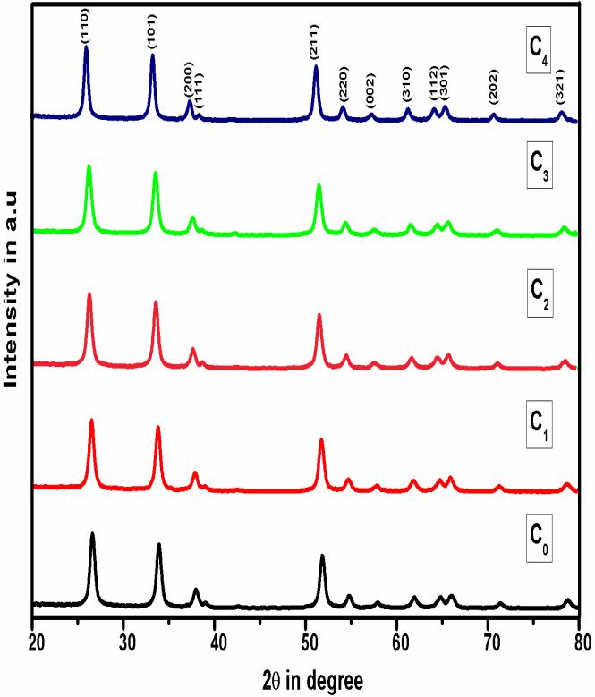
Fig.1 shows the X-ray powder diffraction patterns of Sn1-xCoxO2 nanocrystallites. All the diffraction peaks are well assigned to the tetragonal system of SnO2 with a standard reference pattern (JCPDS # 41-1445) and on doping with Cobalt a similar pattern was observed except that the diffraction peak shifts slightly to the higher angle in comparison to pure SnO2. No extra diffraction peaks from Co or other impurities were detected. It is also observed that the full width at half maxima (FWHM) of the diffraction peaks increases with increase of Co content in prepared samples. The decrease in FWHM along with an increase in peak intensity suggests that by incorporation of dopant into the SnO2 lattice results decrease in grain size of doped tin oxide nanoparticles. The tetragonal distortion (c/a) ratio 0.671, 0.669, 0.667 and 0.678, respectively, calculated for SnO2(C0), Sn0.99Co0.01O
(C
),
samples and their crystallite size 12,11, 10.6, 9 and 8.1nm respectively. The decrement in the values of average crystallite size with Co doping is because of the smaller ionic radii of Co2+ (0.79Å) ion than Sn4+ (0.83Å) ion [19]. Up on doping, as the metal oxide ions occupy the regular lattice site of SnO2, the interference takes place between Co doped metal ions and those of SnO2 lattice, due to the crystalline behavior of the doped metal oxides of SnO2 nanocrystallites, the average grains size tends to reduce than that of pure SnO2 nanostructures. The XRD pattern demonstrates that the products grown are of good crystallinity with the obtained diffraction peaks, broadened by the small nanograins. The grain sizes were estimated from the Scherrer’s relation [20], and the values are tabulated (TABLE I). Lattice parameter values were determined by the least square fit method. A slight variation in the unit cell parameters is observed with the increase of dopant concentration, which indeed indicates that the doped atoms might substitute into the lattice sites of parent atoms.
B. Scanning Electron Microscope (SEM):
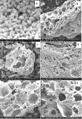
The scanning electron microscopy (SEM) images of the pure SnO2 sample and those doped with 1%, 2%, 3% and 4% cobalt are presented in Figs. 2(a-f) respectively. It can be clearly seen from the SEM images that pure and doped SnO2 have almost spherical shape particles. It is also observed that the porosity of the samples decrease with increase in the Co concentration in SnO2 host matrix and size distribution of nano particles is more uniform throughout the samples.
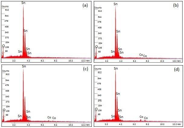
Fig. 3 (a
d) shows the EDAX spectra, collected from the average scanned area, of un‐doped C0, C1, C3, and C4 samples, respectively. The self-generated elemental composition (wt. %) details are also presented in the Fig. 3. It is clear from the figure that Sn, and O are only the main elemental species in pure SnO2 sample while, additionally Co peaks were observed in Co doped samples. However, C peaks, very closer to the O peaks, were also appeared in all the samples. These C peaks were eliminated from the EDAX spectra, during the data analysis, to better examine the O peaks in the spectra. Moreover, the weight percentage of the doped transition metal elements was found to little higher than that of
International Journal of Recent Research in Physics and Chemical Sciences (IJRRPCS)
Vol. 2, Issue 2, pp: (23-30), Month: October 2015 – March 2016, Available at: www.paperpublications.org
nominal concentration, used during the calculations and sample preparation. The atomic percentages of Co as obtained from EDAX are tabulated in TABLE I, which are very close to the starting composition.
D. DC electrical conductivity:
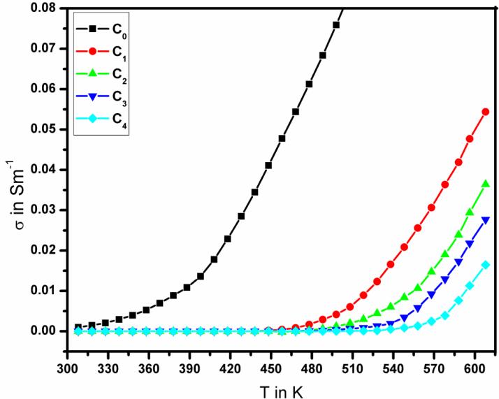
Fig.4 shows the variation of DC electrical conductivity (σ) with temperature (T) for undoped and doped SnO2 nanoparticles in the temperature range of (298–608) K. It is clear from this figure that the conductivity shows the positive temperature coefficient of conductance for all the samples. This indicates the semiconducting behaviour of Sn1-xCoxO2 nanoparticles. The conductivity of the prepared nanoparticles increases with increasing temperature while it decreases markedly as the concentration of Co increases. The increase of the resistivity with the Co concentration indicates a decrease of the number of free charge carriers. When Co atoms are implanted into the host SnO2 lattice, they either occupy interstitial sites or they substitute Sn atoms. In the latter case the Sn atoms can easily move to interstitial sites since the formation energy for Sn interstitial is small [21, 22]. Perfectly stoichiometric SnO2 is an insulator [23] in which four Sn valence electrons are transferred to the oxygen. In real SnO2 a slight oxygen deficiency provides free charge carriers originating from two shallow donor levels due to the oxygen vacancies. Doping with Co inserts ions into the host lattice with a lower valence compared to Sn. This reduces the number of potential binding electrons to neighbouring oxygen atoms. The high electronegativity of the oxygen causes a free-electron capture into the localized acceptor states. Therefore, the conductivity decreases as a function of the Co concentration as shown in the Fig.5.
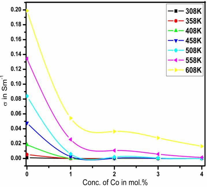
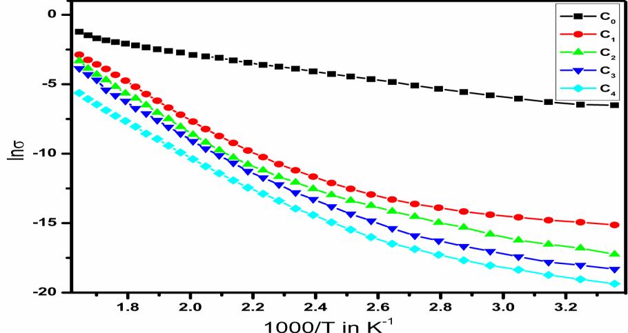
This decrease in conductivity can be understood on the basis of the fact that the conductivity generally decreases when the carrier concentration of the heavily doped semiconductor increases [24]. In order to study the mechanisms of conductivity, it is convenient to plot logarithm of the conductivity ( ln ) as a function of T 1000. Fig. 6 shows the
International Journal of Recent Research in Physics and Chemical Sciences (IJRRPCS)
Vol. 2, Issue 2, pp: (23-30), Month: October 2015 – March 2016, Available at: www.paperpublications.org
relation between of ln versus T 1000for SnO2 doped with different concentration of Co in the temperature range of (298–608) K. It is clear from the figure that the conductivity increases with increase of temperature, such as the general characteristics of the semiconductor with increasing temperature lead to an increase in the number of electron-hole pairs result in an increased conductivity. On the other hand, the plot of ln versus T 1000is nonlinear showing two clear different regions one at relatively high-temperature (480–608) K and the other relatively at low-temperature (308~480) K. This behaviour revealed that the conduction phenomena of the tin oxide proceed through two distinct conduction mechanisms. The conduction mechanism of the activation energy (EAH) at the higher temperatures range (480 K –608 K) is due to carrier excitation into the extended states beyond the mobility edge and at the lower temperatures range (308 K ~ 480 K), the conduction mechanism is due to carrier excitation into localized state at the edge of the band [25] The plots are further analyzed to calculate the activation energies EAH and EAL from the slopes of the straight lines in both regions using equation [26]:
Where σo is the pre exponential factor or temperature independent conductivity, EA activation energy, kB Boltzmann constant, and T temperature.
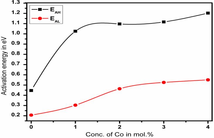
The activation energy of the samples can be determined from the slopes of the straight lines in Fig. 6. The analysis of the conductivity data yields the activation energies of the donor levels, which are given by an Arrhenius plot. For all doping concentrations two activation energies can be derived as shown in the Fig. 7. In all samples a very low donor level may be attributed to interstitial Sn [21].The roughly constant intermediate (EAH) and increasing high values (EAL) can be assigned to oxygen donors [27].The increase of the activation energies with the Co doping concentration results from a considerable coulomb attraction between the electron and the ionized impurities which increase with the donor concentration [28]
International Journal of Recent Research in Physics and Chemical Sciences (IJRRPCS)
Vol. 2, Issue 2, pp: (23-30), Month: October 2015 – March 2016, Available at: www.paperpublications.org
Fig. 7 shows the effect of Co content on both activation energies EAL and EAH for SnO2 samples. It was observed that the activation energies increase with the increase of Co concentration may be due to change in the localized states, structure, and composition of samples as well as to the rearrangement of atoms which yields fewer defects [29].
IV. CONCLUSION
Sn1-xCoxO2 nanoparticles have been successfully prepared by the gel combustion method. The XRD patterns exhibit the tetragonal rutile structure of all the samples with no impurity phase. On Co doping, a shift in the diffraction peaks towards the higher diffraction angle which indicates that Co ion has substituted the Sn site without changing the rutile structure. The doping of Co in SnO2 not only lowers the crystallite size but also degrades the crystallinity of the nanoparticles. The atomic percentages of Co obtained from EDAX which are very close to the starting composition. The DC conductivity of the Co doped SnO2 samples increases with temperature and decreases with the increase of dopant concentration at different temperatures while activation energy increases with dopant concentration. From this one can concluded that Cobalt dopant enhances the resistivity of tin oxide nanoparticle or expected to induce a negative impact on the electrical transportbehaviour.
ACKNOWLEDGMENT
The authors would like to acknowledge their sincere thanks to Dr. R. Somashekhar, Department of Physics, Manasagangotri, University of Mysore for providing XRD facility and Department of Material Engineering, Indian Institute of Science, Bangalore for the EDAX and SEM facilities.
REFERENCES
[1] J. T. Hu, M. Ouyang, P. D. Yang & C.M. Lieber. “Controlled growth and electrical properties of heterojunctions of carbon nanotubes and silicon nanowires,” Nature; vol.399, pp. 48-51, 1999
[2] B. Sathyaseelan, K. Senthilnathan, T. Alagesan, R. Jayavel, K. Sivakumar, “A study on structural and optical properties of Mn and Co-dopedSnO2nanocrystallites,” Mater. Chem. Phys. Vol. 124, pp. 1046-1050, 2010
[3] J. Kappler, A. Tomescu, N. Barsan, V. Weimar, “CO consumption of Pd doped SnO2 based sensors,” Thin Solid Films; vol. 391, pp. 186-191, 2001
[4] R.K. Mishra, P.P. Sahay, “Synthesis, characterization and alcohol sensing property of Zn-doped SnO2 nanoparticles, Ceram. Int., vol 38, pp. 2295-2304, 2012.
[5] G. Zhang, M. Liu, “Effect of particle size and dopant on properties of SnO2-based gas sensors, Sens. Actuators: B, vol. 69, pp. 144-152, 2000
[6] M Batzill, U Diebold, “The surface and materials science of tin oxide. Prog Surf. Sci., 79, 47-154, 2005
[7] Chiu HC, Yeh CS. “Hydrothermal synthesis of SnO2 nanoparticles and their gas-sensing of alcohol,” J. Phys. Chem., 111:7256-7259, 2007
International Journal of Recent Research in Physics and Chemical Sciences (IJRRPCS)
Vol. 2, Issue 2, pp: (23-30), Month: October 2015 – March 2016, Available at: www.paperpublications.org
[8] T.P. Hülser, H. Wiggers, F.E. Kruis, A. Lorke, “Nanostructured gas sensors and electrical characterization of deposited SnO2 nanoparticles in ambient gas atmosphere,” Sens. Actuators B, vol. 109, pp. 13-18, 2005.
[9] A. Azam, A.S. Ahmed, M.S. Ansari, M. Shafeeq, A.H. Naqvi, “Study of electrical properties of nickel doped SnO2 ceramic nanoparticles,” J. Alloys Compd. Vol. 506, pp. 237-242, 2010.
[10] V. Golovanov and A. M. Matti, Experimental and theoretical studies of indium oxide gas sensors fabricated by spray pyrolysis,” vol. 106, pp. 563
571, 2005
[11] H. Kimura, T Fukumura, M. Kawasaki, K. Inaba, T. Hasegawa & H. Koinuma, Rutile-type oxide-diluted magnetic semiconductor: Mn-doped SnO2. ” Appl Phys Lett., vol. 80, pp. 94-96, 2002
[12] R. Maity, S. Kundoo, K.K. Chattopadhyay, . Synthesis and optical characterization of CdS nanowires by chemical route. Materials and Manufacturing Processes,” vol. 21, pp 644–647, 2006
[13] R. Rai, T. D. Senguttuvan, S.T. Lakshmikumar. Study of the electronic and optical bonding properties of doped SnO2,” Comput. Mat. Sci. vol. pp. 37, 15–19, 2006.
[14] A. E. Owen, in: J. E. Burke (Ed.), Progress in Ceramic Science. 3rd ed. Macmillan, New York, pp. 77– 196, 1963.
[15] Joseph George, C.S. Menon, “Electrical and optical properties of electron beam evaporated ITO thin films,” Surface and Coatings Technology, vol. 132, pp. 45-48, 2000
[16] E. Benamar, M. Rami, C. Messaoudi, D. Sayah, A. Ennaoui, “Structural, optical and electrical properties of indium tin oxide thin films prepared by spray pyrolysis,” Solar Energy Materials and Solar Cells, vol. 56, pp. 125-139, 1999
[17] Yinzhu Jiang, Wenping Sun, Bin Xu, Mi Yan. Naoufal Bahlawane, “Unusual enhancement in electrical conductivity of tin oxide thin films with zinc doping,” Phys. Chem. Chem. Phys. vol. 13, pp. 5760–5763, 2011.
[18] J. H. Kang, Y. Kim, and D. Young, “Synthesis and Characterization of Orange-Emitting SnO2 : Eu+3 Phosphor by an Optimized Combustion Method,” Journal of The Electrochemical Society, vol. 152, pp. 33
38, 2005.
[19] Nadir Fadhil Habubi, Ghuson H.Mohamed, Saad Farhan Oboudi, Sami Salman Chiad, “Structural and electrical properties of cobalt doped SnO2 thin films,” PCAIJ, vol. 9(5), pp. 169-174, 2014
[20] V. Golovanov and A. M. Matti, “Experimental and theoretical studies of indium oxide gas sensors fabricated by spray pyrolysis,” vol. 106, pp. 563–571, 2005
[21] C. Kilic,A.Zunger, “Origins of coexistence of conductivity and transparency in SnO2, ” Phys.Rev.Lett., vol. 88, pp. 095501-1 - 095501-4, 2002
[22] A. Awada, D.Menzel, H.Dierke, J.Schoenes, F.Ludwig,M.Schilling, “Free-carrier compensation in ferromagnetic ion-implanted SnO2:Co,” J. of Appl. Phys., vol. 07 , pp. 103-106, 2008.
[23] C. Terrier, J.P.Chatelon, R.Berjoan, J.A.Roger, “Sb doped SnO2 transparent conducting oxide from the sol-gel dipcoating technique,” Thin Solid Films, vol. 263, pp. 37- 41, 1995
[24] S.Y.Lee, B.O.Park, Structural, electrical and optical characteristics of SnO2: Sb thin films by ultrasonic spray pyrolysis. Thin Solid Films, vol. 510, pp. 154-158, 2006
[25] J. I. Langford, A.J.C.Wilson, “Scherrer, Scherrer after sixty years: survey and some new results in the determination of crystallite size,” J.Appl.Cryst. 1978; 11: 102-113.
[26] M. P. Rajeeva, C. S. Naveen, Ashok R. Lamani, V. Prasad Bothla, and Jayanna HS. Conf. Proc., vol. 1665, pp. 050091-1–050091-3, 2015
[27] S. Samson, C.G.Fonstad, “Defect structure and electronic donor levels in stannic oxide crystals,” J.Appl.Phys., vol. 44, pp. 4618-4623, 1973.
[28] G. L. Pearson, J. Bardeen, “Electrical properties of pure silicon and silicon alloys containing boron and phosphorus,” Phys.Rev., vol. 75, pp. 865-883, 1949
[29] H. He Jr., Te H.Wu, Cheng L.Hsin, Kun M.Li, Lih J.Chen,Yu L.Chueh, “Beak like SnO2 nanorods with strong photo luminescent and field emission properties,” small, vol. 2(1), pp. 116-120, 2006