The Brief
ENGINEERING FOR GLOBAL IMPACT
AT NORTHEASTERN UNIVERSITY


The demand for semiconductor production is booming while exciting innovations leading to ultra-tiny, more powerful, and lower-cost chips are creating unprecedented applications to benefit society across industry sectors. Think wearable medical devices, increased AI processing capacity, mainstream quantum computers, and 5G and beyond wireless communications, to name a few.

The Institute for NanoSystems Innovation at Northeastern University is leading the charge to develop future semiconductor and related technologies—sensors and actuators, signal processing and AI, wireless and electronics—and drive innovation and nanoscale miniaturization with an open innovation environment. In collaboration with industry and government, the institute is reshaping the landscape of chip-level technology advancements and applications, and piloting manufacturing, while training the next-generation of talent.
Read on to learn more and I invite you to reach out with ideas for collaboration and more information.
Kind regards,
Gregory D. Abowd, D.Phil. Dean of the College of Engineering Northeastern University coe.northeastern.edu

Institute for NanoSystems Innovation
Groundbreaking 3D Imaging System for Early Cancer Detection
Novel High-Speed MEMS Sensor To Revolutionize Navigation Systems
Powering the Next Generation of AI Applications at Nanoscale

Revolutionizing Signal Processing With New Acoustic Wave Technologies
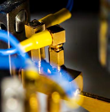
Patented Nanomanufacturing Process Slashes Chip Production Costs by 99%

Creating SemiconductorScale Quantum Computer Components
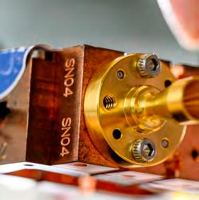
Outsmarting Terahertz Band Obstacles for Mainstream 6G Communications
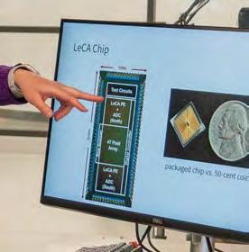
Integrated Vision System To Surpass That of the Human Eye

Redefining the Future of Computing With Engineered All-Optical Photonic Chips

Dormant but Always-Alert Sensors To Power the ‘IoT Grid’
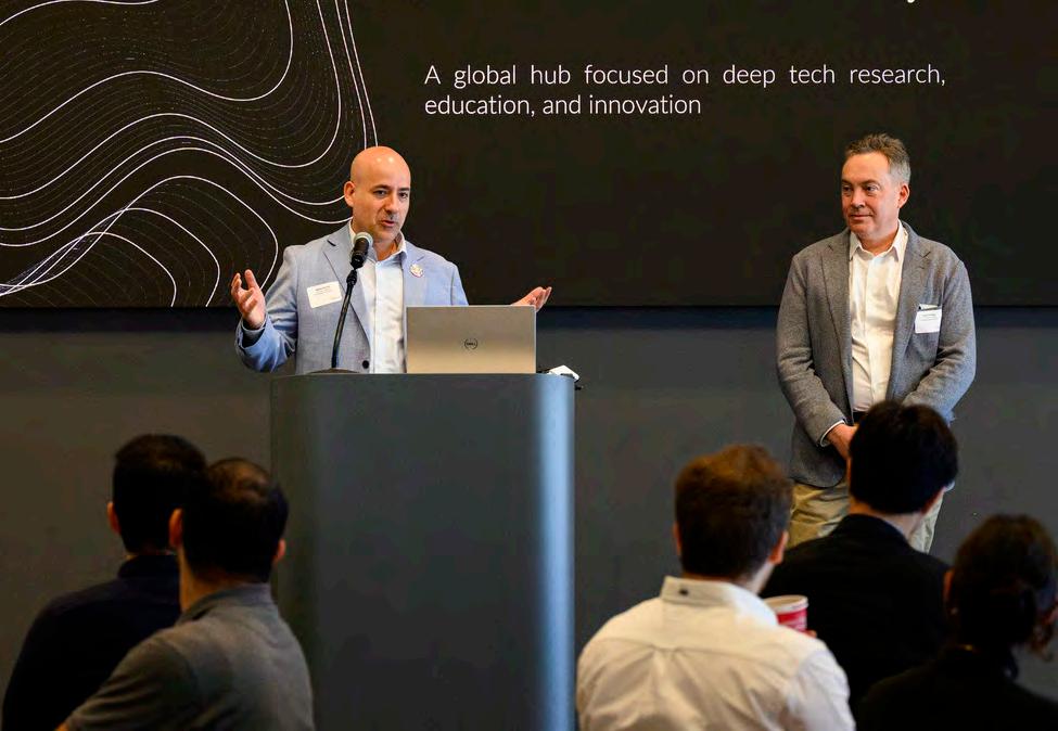
A medical device that can help determine if you have cancer but can fit on the pad of a fingertip. Miniaturized radio frequency devices to enable 5G technology and beyond. Wearable and implantable sensors. Quantum computing. These are just some of the future capabilities made possible by semiconductor innovation and nanotechnology—technology measured on the scale of a nanometer, one-billionth of a meter.
To put one-billionth of a meter in perspective, a strand of human hair is between 80,000 and 10,000 nanometers wide, while a strand of human DNA is only 2.5 nanometers wide, according to the National Nanotechnology Initiative. To develop future domestic semiconductor technologies and drive innovation and miniaturization at this scale across a wide range of functions, Northeastern University launched the first-of-its-kind Institute for NanoSystems Innovation (NanoSI), located on its campuses on both coasts of the United States—Boston and Burlington, Massachusetts, and Oakland, California.
Matteo Rinaldi and David Horsley, professors of electrical and computer engineering, are co-directors of the institute. Together with their interdisciplinary team of 22 faculty and over 150 other researchers, and through an open innovation environment enabling partnerships between university, industry, and government stakeholders, they aim to reshape the landscape of chip-level technology advancements and applications.
Leveraging Northeastern’s global campus network, NanoSI focuses on research, education, and entrepreneurship in semiconductors and related technologies. Research involves designing, manufacturing, testing, and validating the tiny silicon chips crucial to advanced technologies. NanoSI receives more than $20 million annually in federal and industry funding and is home to leading national programs supported by DARPA, ARPA-H, ARPA-E, DoD, DHS, and NSF in RF and mmWave devices and systems, ultra-low power sensors, advanced functional materials, nanophotonics, nanomedicine, artificial intelligence, quantum devices and systems, and microelectronics for medical devices.
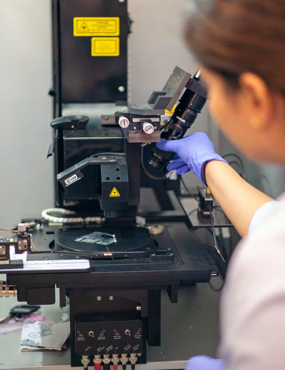

Electrical, mechanical, and optical testing
- Micro/nano systems
- Superconducting electronics
- Silicon photonics
- RF
- mmWave
- THz devices and systems
Clean rooms – capable of processing 150 mm and 200 mm wafers
The integrated circuit was invented in the U.S. in 1958, and Silicon Valley venture capitalists quickly organized to fund startups to commercialize this technology as early as the 1960s. In recent years, however, U.S. venture capital investment shifted its focus to software because software development is faster and provides a quicker return on investment. With that, the bulk of semiconductor manufacturing moved to Asia. The result? A shortage of semiconductor talent.
“Semiconductors,” says Rinaldi, are the “brains and senses of modern electronics.” For example, AI places high demand on semiconductors because AI applications process and store massive amounts of data. Nearly every sector of business and industry needs smaller and more powerful semiconductor chips, from wireless communications to car manufacturers to consumer electronics.
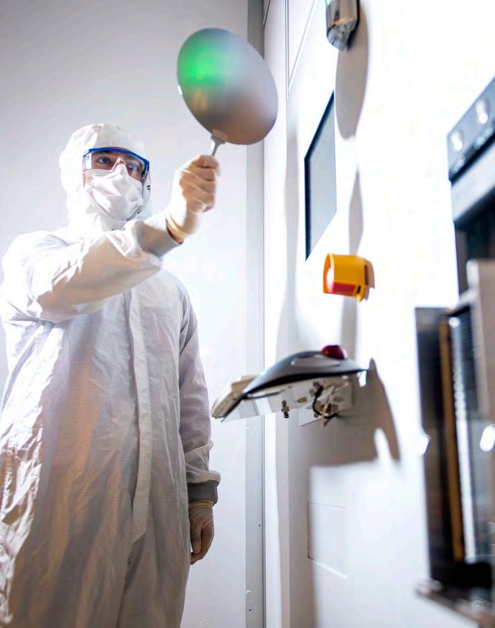
Researchers and partners of NanoSI have unique experimental capabilities, including a 15,000 square-foot laboratory in Boston with state-of-the-art electrical, mechanical, and optical testing capabilities for micro/nano systems, superconducting electronics, silicon photonics, RF, mmWave, and THz devices and systems. In addition to an existing cleanroom on Northeastern’s Boston campus, which is capable of processing 150 mm and 200 mm wafers, a new 20,000 square-foot cleanroom is planned for Northeastern’s Innovation Campus in Burlington, Massachusetts. NanoSI facilities are also on the Oakland, California campus, an ideal location near Silicon Valley. The facilities include laboratory space, offices for six faculty members and workspaces for 26 graduate students and postdoctoral researchers, and a collaboration with University of CaliforniaBerkeley’s cleanroom. Additionally, Horsley says, “We believe NanoSI is—or will soon be—the largest university center for micro-electromechanical systems (MEMS) research in the U.S.”
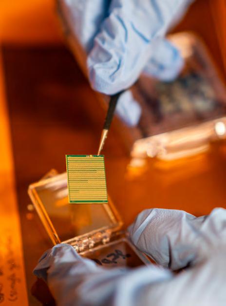
To develop future domestic semiconductor technologies and drive innovation and miniaturization across a wide range of applications, Northeastern University launched the first-of-its-kind Institute for NanoSystems Innovation (NanoSI), located on its campuses on both coasts of the United States. visit nanosi.northeastern.edu
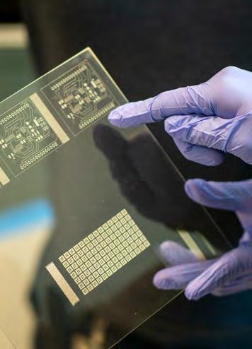
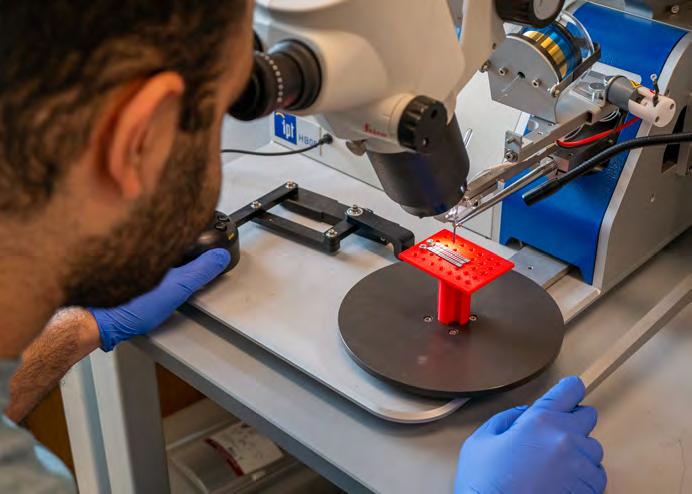
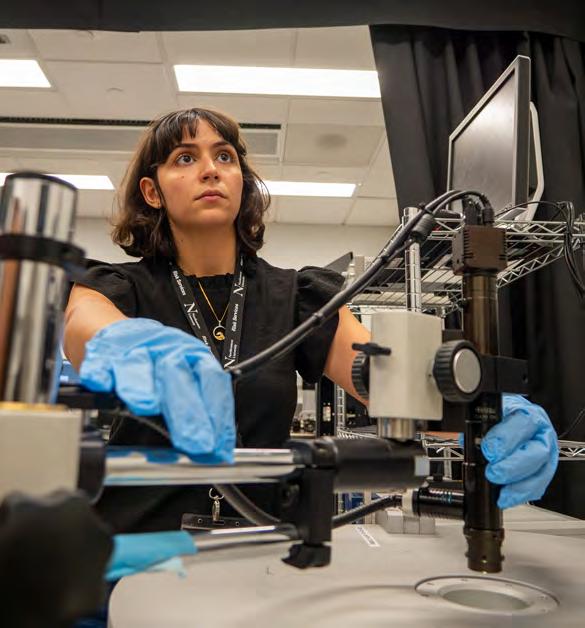
Part of NanoSI’s mission is to help the U.S. become chip independent at a time when demand for chips is growing exponentially and the federal government is investing in the domestic semiconductor industry. The U.S. CHIPS Act—Creating Helpful Incentives to Produce Semiconductors—which was signed in 2022, allocated $50 billion to U.S. startups and industry.
NanoSI is addressing this growing demand by partnering with industry and government to pilot manufacturing and drive innovative design. Rinaldi says there is a bottleneck in the semiconductor industry that emerges from a shortage of talent on one side and, on the other, misalignments between research and development laboratories “where the innovation typically initiates,” and large-scale manufacturing and fabrication. “These new technologies come with new challenges,” he explains.
Rinaldi notes, “Our objective is to really open this bottleneck” by leveraging Northeastern’s experiential learning and co-op programs to provide “hands-on training of the workforce,” as well as its global network of campuses and researchers, and by “providing industry-compatible” instruction to “bridge that lab-to-fab gap.” Horsley, who is an experienced semiconductor startup entrepreneur, hosts topic-specific and startup innovation workshops for researchers and industry locally and globally, most recently in Taiwan and with a second workshop planned for Singapore.
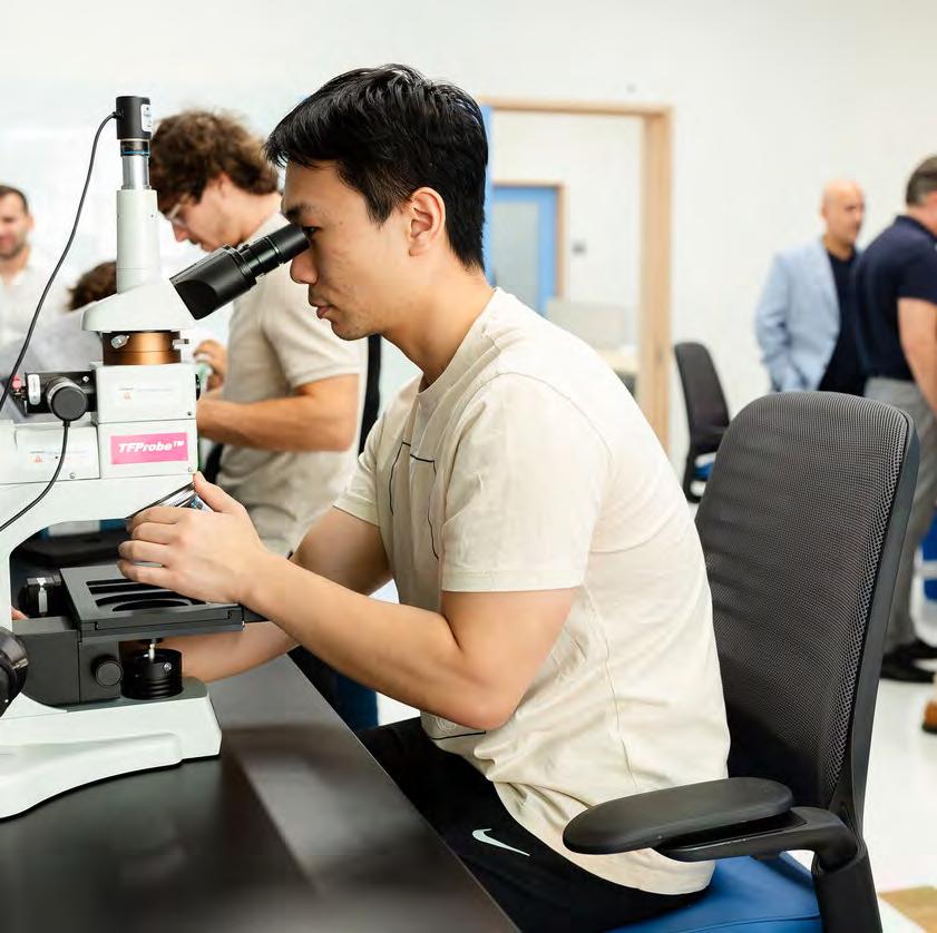
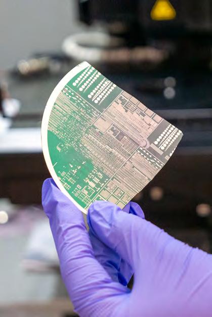
To develop next-generation talent through education, NanoSI, along with the College of Engineering at Northeastern, is launching an MS in semiconductor engineering degree in 2025. Also, the PhD in electrical engineering expanded to the Oakland campus where doctoral students conduct research as part of NanoSI. For undergraduate second-year students, NanoSI offers a Semester In program where they spend a semester in Oakland learning about semiconductors as the engines of AI.
To meet education and research growth in Oakland, two assistant professors of electrical and computer engineering joined in January 2025. Professor Aravind Nagulu’s research focuses on application-specific integrated circuits, and Professor Yuan Yuan’s research is on optoelectronic devices, single-photon detection, silicon photonics, and large-scale photonic integrated circuits.
NanoSI has established researchers with decades of experience, as well as young faculty members who are getting established in—and disrupting—their field. “When you engage with us,” Horsley says, “you can access well-known experts and also engage with rising stars who are early in their career and devoted 100% to their research.” N
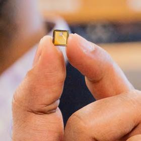
The most advanced semiconductors in development today cannot vault us into new realms of AI applications, autonomous air and ground transportation, and virtual reality if they don’t have enough power to get the job done.
With a $2 million award from the National Science Foundation, a team led by Aatmesh Shrivastava, associate professor of electrical and computer engineering, is developing a next-generation nanoscale power supply system for semiconductors to help solve this problem. The team is also collaborating with Cornell University researchers.
“The power needed by AI and other applications for high-performance computing will exceed the power that we can produce on Earth by 2040 to 2050,” says Shrivastava. “Right now, power delivery is a huge bottleneck.”
The new power supply system uses novel materials that enable a compact insulated design. A unique spin spray deposited ferrite process applies the magnetic material necessary to conduct electricity in a thin, uniform layer on power system components. This enables the components to be developed at a nanoscale level and insulates them, so they lose only a small amount of electricity as they are delivering it to a system’s central processing unit. The power supply system will also have an integrated architecture to support inductors, transformers, switches, and complementary-metal-oxide semiconductor (CMOS) control circuitry, which operates more efficiently than current technology.
A new nanoscale power supply system for semiconductors uses novel materials for a compact and insulated design, increasing efficiencies far more than current technology.
At the heart of this research is the spin spray deposited ferrite process, which has enabled the nanoscale design. In contrast, today’s power supply systems use bulkier magnetic materials built on metal surfaces to conduct electricity. The new power supply system will be measured in millimeters, an order of magnitude smaller than today’s systems, which are measured in inches. As a result, the new system will be able to fit adjacent to most central processing units.
The small size has enabled a vertical architecture design so the power supply system sits directly below the processor, which will result in faster and more efficient delivery of power. Because today’s systems are so much larger, they are typically assembled in a lateral structure at least a few inches away from the processor.
The distance between processor and power supply is game changing. Current systems can lose up to 30% of the electricity as they are transporting it to the processor. The new system will drop only about 1% of the power it transmits. Additionally, the ferrite materials are insulated to further prevent power loss.
While the research stands to impact any industry that will continue to need more and more power, it also addresses environmental concerns. Because the power supply system will drop far less electricity in transmission than current systems, it will actually lead to transmitting less electricity overall to meet the power demand. These efficiencies mean less fossil fuel usage to create electricity. N

“The power needed by AI and other applications for high-performance computing will exceed the power that we can produce on Earth by 2040 to 2050.”
Aatmesh Shrivastava associate professor of electrical and computer engineering
In the quest to deliver more data at faster speeds, the next frontier is the terahertz (THz) band, where 6G communication is expected to operate. Sitting between microwave and infrared light frequencies, terahertz has the potential to send data at speeds of up to hundreds of gigabits per second.
If only there weren’t so many obstacles in the way.


At such a high frequency, signals traveling in the terahertz band interact with more of their surroundings than signals on lower-band frequencies. The issue is with the photons, which are the smallest possible particles of electromagnetic energy and, therefore, also the smallest possible particles of light. They carry the data and become increasingly active as the frequency increases. At the terahertz level, these particles are interacting with obstacles of all kinds, from walls and furniture to pets and plants. The encounters end up degrading signal performance because the obstacles can absorb the particles, slow them down, or reflect them back to their source.
“These signals don’t propagate well,” says Josep Jornet, professor of electrical and computer engineering and associate dean for research, who is a wireless technology expert.
Jornet is developing a system to essentially outsmart the obstacles so the signals can get to their destination at the speeds the terahertz realm promises. He is designing an on-chip programmable electromagnetic surface (PES) that will capture a signal and then direct it to its destination using one of several methods. A PES is a specially designed surface composed of tiny, electronically controlled elements that can manipulate the behavior of electromagnetic waves. The PES Jornet is developing sits between the transmitter and receiver of a communications line and could be installed on a wall.
A key element to the research is developing AI algorithms that can be trained in critical terahertz communications and sensing functions to identify issues and deploy the best method to work around the signal’s obstacle. One method would be to reroute or bend the signal. Another approach is to adapt the signal with a self-healing capability that can regenerate portions of the signal that are lost when colliding with an obstacle.
“Even if an obstacle doesn’t block an entire signal, part of it may be lost, but with the PES we can regenerate what’s lost,” Jornet says. “The signal reshapes itself.”
The PES will include an antenna and an array of reflectors, each less than a millimeter in size and each with a corresponding controller. It will be the first to embody the hybrid integration of nanometer-scale hafnium zirconium oxide, which has ferroelectric properties, and graphene materials, resulting in components with a thickness of 20 millimeters or less.
Jornet’s research is funded by a $500,000 grant from the Air Force Office of Scientific Research. He is collaborating with Cristian Cassella, associate professor of electrical and computer engineering, and Benyamin Davaji, assistant professor of electrical and computer engineering.
The technology could initially be used on military airplanes and satellites and could play a role in deflecting and redirecting communications signals. More broadly, these devices could eventually be used in homes and offices, bringing the terahertz frequency to the mainstream. N

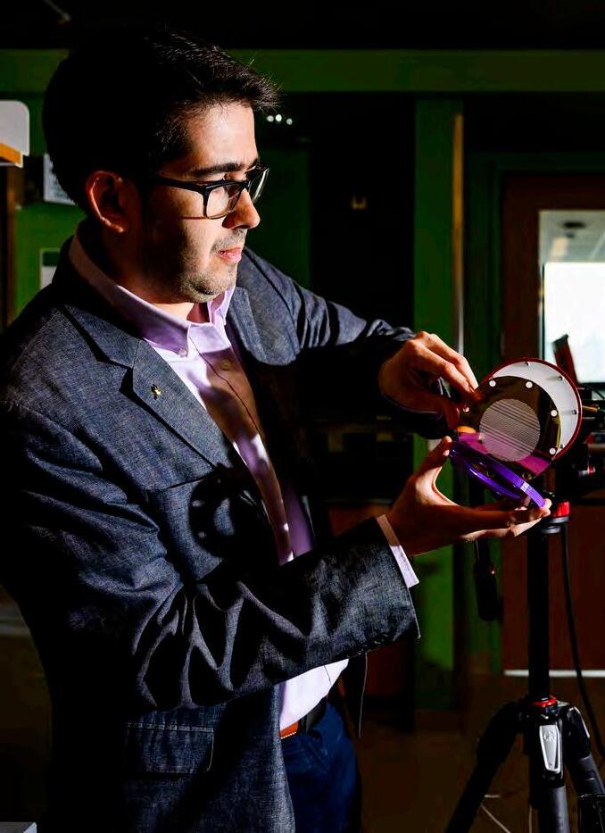
A novel on-chip programmable electromagnetic surface (PES) with nano-scale components will use AI algorithms trained in critical terahertz communications and sensing functions to identify and work around photon obstacles so signals get to their destination at speeds the terahertz realm promises.

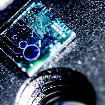
In the United States, more than 360 people die from lung cancer every day and it is the deadliest form of cancer, according to the American Lung Association. Soner Sonmezoglu, assistant professor of electrical and computer engineering, is determined to change these grim statistics.
An expert in integrated circuits and microfabrication, Sonmezoglu is leading a multi-institutional research team to develop a first-of-its-kind electronic photonic photoacoustic imaging system that could redefine how lung cancer is diagnosed. His work is funded by up to $13.2 million from the Advanced Research Projects Agency for Health (ARPA-H), which supports high-risk, high-impact research projects with the potential to bring about major breakthroughs in healthcare. Sonmezoglu is the first Northeastern faculty member to receive funding from ARPA-H and his project team includes Matteo Rinaldi, professor of electrical and computer engineering and director of the Institute for NanoSystems Innovation, Massachusetts General Hospital, Johns Hopkins University, and the University of Washington.
Focused on heterogeneous integration, the research brings together the power of photonic chips, which process data using light instead of electricity, enabling them to be designed on a nanoscale level, and micro-electro mechanical components. Sonmezoglu says, “The integration enables extreme miniaturization of the probe that touches the lung tissues through a bronchoscope without degrading the imaging resolution. It is more than an order of magnitude smaller than the other probes that exist today.”
The problem is that current imaging techniques do not have high enough resolution to determine whether tumors in their early stages are malignant or benign without the aid of a biopsy. And biopsies can have a lot of complications. The invasive procedure could nick the lung and cause it to collapse, and the use of MRI and CAT scan machines are costly and not portable.
Sonmezoglu’s imaging system will produce real-time, 3D high-resolution images with far greater detail of a tumor than today’s systems and enable a safer and less costly procedure for patients. The system will also be small and portable, the size of a trash can.
“We can probe very small tumors, and if we can determine it is malignant, that patient is going to have a real high chance of survival.”
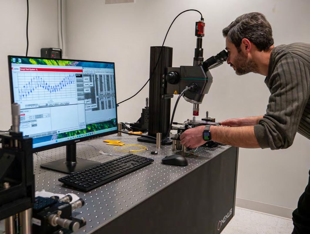
Using a tiny probe with a width of only 1.5 millimeters—similar in size to a grain of rice—the system applies light to the tumor without penetrating the lung tissue. The light causes the tumor’s cells to react, creating highfrequency signals. The probe essentially functions as an optical acoustic detection unit and captures and relays those signals to the image processing component of the system.
“Conventional systems can only capture the signals around 5 or 6 megahertz, but the technology we are building is going to capture signals at around 20 megahertz,” Sonmezoglu says.
The probe can transmit the signals at such a high frequency that the imaging component is able to render images with exceptional detail. The imaging reveals key attributes of a tumor’s vascularity, oxygen saturation, and collagen—all critical information that help determine if the tumor is malignant or benign. “Those three parameters are going to enable us to differentiate the malignant nodules from the benign ones,” Sonmezoglu says.
The system could revolutionize medical diagnostics beyond lung cancer detection, including other cancers as well as cardiovascular diseases. As it provides in-depth details about a tumor at an early stage, it stands to save countless lives. Sonmezoglu says, “It can probe very small tumors and if we can determine if it is malignant, that patient is going to have a real high chance of survival.”
A critical success factor to the research has been collaboration with experts in pathology, surgery, and engineering from multiple institutions in addition to the Northeastern team. “Working with MGH and Johns Hopkins, we will have access to many medical doctors whose guidance and input will help in the design and faster adoption in the clinical environment,” Sonmezoglu says. N
All modern wireless communication—from radios to cellphones—engages in a process of translation. Radio frequency signals are picked up by an antenna, and components behind the antenna translate those frequencies into an electrical signal, whether analog or digital.
Called signal processing, devices “need to be able to distinguish the signal from the noise,” says Siddhartha Ghosh, assistant professor of electrical and computer engineering. “For you to be able to simultaneously support various channels of communication,” he continues, “like voice and text and data and all that stuff, you need to be able to isolate those bands.”
“Signal processing basically refers to the ability to isolate those signals from a noisy background using different approaches,” Ghosh says. And the modern wireless world is very noisy. There are innumerable signals traveling through the air at any given moment—even at-home Wi-Fi networks use radio frequencies to transmit information. It takes a feat of (micro) engineering to develop devices that can parse between these intermingling signals and convert them into something a device like your cellphone can then read as a text message or incoming phone call.
Ghosh notes that a variety of components sit behind the antenna, called radio frequency front-end (RFFE) devices, like “filters, amplifiers, and mixers.” The specific components Ghosh designs enable signal translation by manipulating “acoustic waves in solids,” he says.
By converting a radio frequency, which is in the electrical domain, into a physical vibration through a solid material, it travels as a sound wave across what’s called a piezoelectric material. But these aren’t the kind of sound waves you can hear. Vibrating at the scale of a microchip, these analog vibrations can be read and converted to a digital signal by other components farther downstream. Because acoustic waves travel much slower than the speed of light by about five orders of magnitude, Ghosh says, “the filters that are utilized using acoustic waves have certain benefits over the competing legacy technologies that would involve discrete components such as inductors and capacitors,” including compact form factors and the ability to store energy more efficiently.
Ghosh also works on interfacing these acoustic waves with light that is guided on a chip. Using acoustic waves in materials like aluminum nitride, Ghosh and his team can route and control the flow of light modulating optical signals for more specialized needs.
In support of this research, Ghosh received two prestigious young investigator awards. The Defense Advanced Research Projects Agency Young Faculty Award is for creating single-platform microsystems that can incorporate active functionality with passive acoustic wave devices at radio frequencies.
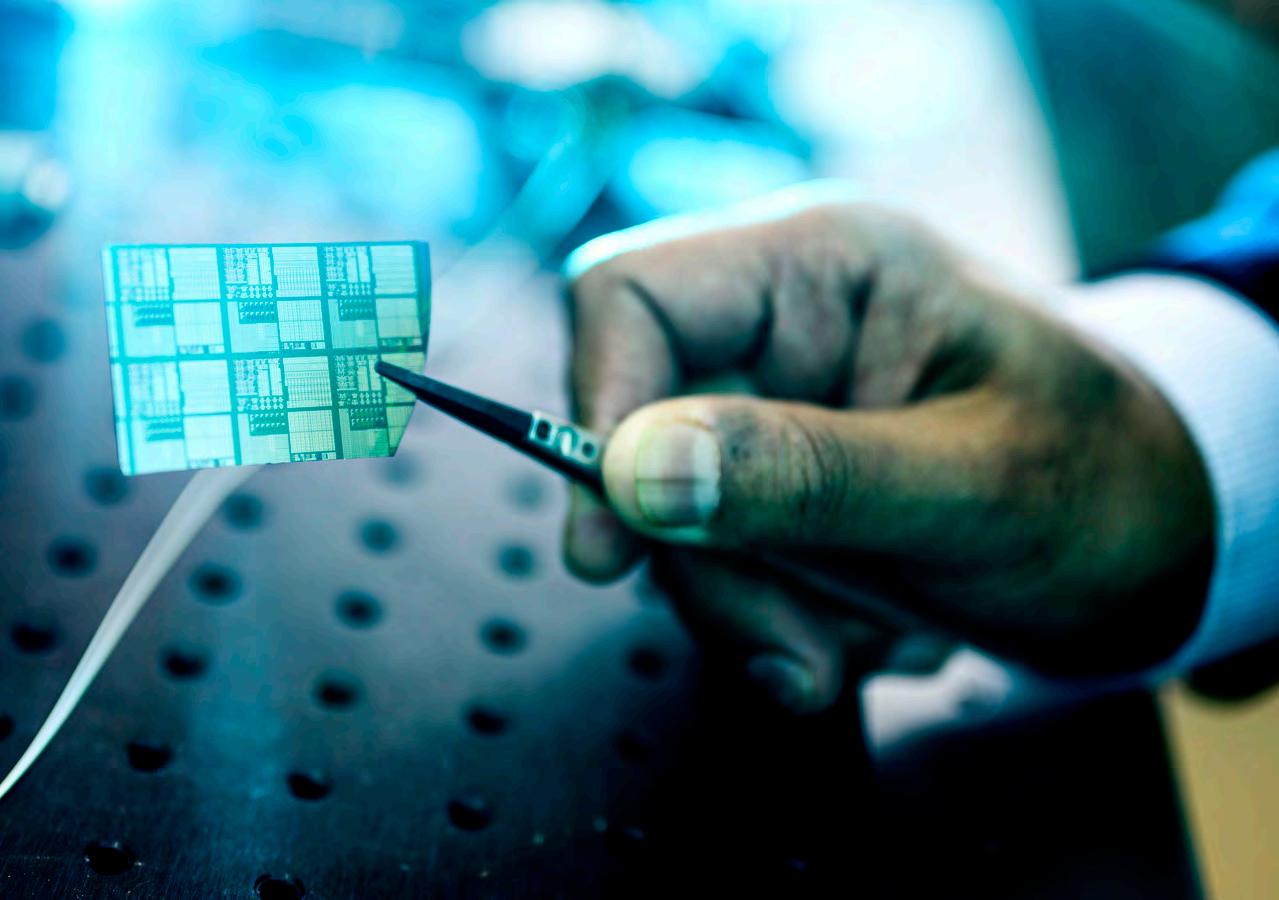
“We envision devices that can process signals in multiple physical domains but don’t require increased complexity in fabrication and manufacturing, bringing down both costs and device sizes.”
Siddhartha Ghosh
assistant professor of electrical and computer engineering

“By developing a single platform for all-acoustic RF signal processing covering high frequency through super-high frequency bands, we can unlock new potential in acoustic wave devices with improved radio receivers and chip sets, reduced system complexity, and more resilience to intentional third-party signal interference,” explains Ghosh. He is also developing full duplex communication systems—the ability to transmit and receive at the same time.
With a National Science Foundation CAREER Award, Ghosh is developing a novel microsystem on-a-chip platform that seamlessly integrates acoustic, optical, and electric fields, and is highly configurable to be used in a range of RFFE signal processing devices and materials.
The integrated signal processing capability enables multiple domains to be manipulated at the same time, resulting in more efficient processing and spectrum utilization. It will reduce costs, enhance performance, and extend RF communications and information processing capabilities, particularly for optical communications and in quantum computing. N
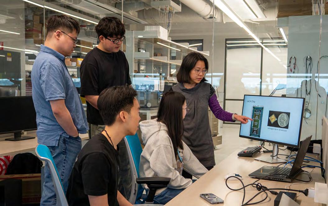
High-end imaging systems can produce images with levels of detail and shades of light that are breathtaking, but they still can’t capture all that a human can see or interpret visual scenes based on the scene’s context.
Now a multi-institutional team of researchers, led by Xuan “Silvia” Zhang, associate professor of electrical and computer engineering, is designing an integrated vision system with nanoscale components that not only intends to outdo the state-of-theart of imaging technology, but also plans to surpass the capabilities of the human eye.
“We are completely reimagining how we can design a vision system,” Zhang says. “Unlike traditional camera and imaging systems that are designed for human visual consumption, we aim to create an entirely new vision system that is tailored for algorithms running on machines.”
With a $2 million award from the National Science Foundation, Zhang, in collaboration with the University of Rochester, Washington University in St. Louis, and University of Illinois, is developing a novel design model for an AI-based vision processing system. It integrates a nanoscale optical element that captures and preprocesses light, an image sensor with built-in computing capabilities, and a tailored digital vision processor. The goal is to eventually build a single-chip version that will measure about the size of a postage stamp.
“This will open up so many possibilities because it will enable us to use information beyond human visibility,” Zhang says. “Just imagine how that could empower applications.”
“Using nanotechnology, AI, and computational image sensors, we are completely reimagining how we can design a vision system.”
Xuan “Silvia” Zhang associate professor of electrical and computer engineering

Traditional advancements to the image-capture process have focused on boosting pixel counts or video frame rates. This system forgoes that approach and relies on AI algorithms that train the system to capture only pertinent information about an image, weeding out backgrounds and other extraneous image data. By winnowing the image data down to only features that the system needs to assess the attributes of the image and carry out the vision tasks, the amount of data transmitted and processed will be substantially reduced. This will also reduce energy consumption.
Zhang says the system will capture about 5% of data as compared to the image’s original pixel size because the algorithms will be trained to learn image attributes and apply that knowledge to subsequent images. The system could eventually be used in a wide range of applications currently relying on imaging technology, from medical diagnostics and factory floor operations to surgical robotics and security cameras.
Each research team member is bringing specific expertise to the project. Zhang is focused on the co-design of the image sensors with the vision algorithm. Through collaborative development, each individual system component is integrated and designed to enhance other components’ performance. As an example, the team is exploring how to best distribute computation throughout the vision system pipeline to avoid processing lags.
To help advance competitiveness in the global semiconductor industry, the team is collaborating with colleges and industry partners to provide workforce development, mentorship programs, and curriculum. “This is for people who are interested in getting into this field or who may need to retool their skillsets to learn about the different domains that are part of this integrated machine vision system,” Zhang says. N
View Research Paper from ACM/IEEE ISCA Symposium
Y. Feng, T. Ma, Y. Zhu and X. Zhang, “BlissCam: Boosting Eye Tracking Efficiency with Learned In-Sensor Sparse Sampling,” 2024 ACM/IEEE 51st Annual International Symposium on Computer Architecture (ISCA), Buenos Aires, Argentina, 2024, pp. 1262-1277, doi: 10.1109/ ISCA59077.2024.00094.
by
View Research Paper from IEEE/ ACM ICCAD Conference
Y. Feng, T. Ma, A. Boloor, Y. Zhu and X. Zhang, “Invited Paper: Learned In-Sensor Visual Computing: From Compression to Eventification,” 2023 IEEE/ ACM International Conference on Computer Aided Design (ICCAD), San Francisco, CA, USA, 2023, pp. 1-9, doi: 10.1109/ ICCAD57390.2023.10323842.
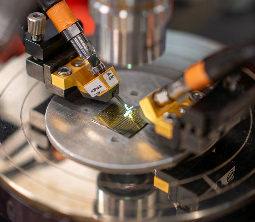
Military and commercial vehicles can experience an ultra-wide range of accelerations, making it extremely difficult for them to rely on existing sensor technologies for navigation and positioning in GPS-denied environments. While these sensors can withstand shocks, they do so at the expense of reduced sensitivity to small accelerations, ultimately compromising their positioning and navigation capabilities.
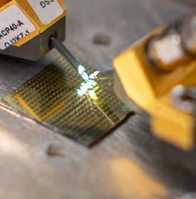
Now a research team, led by Cristian Cassella, associate professor of electrical and computer engineering (ECE), is building a microelectromechanical (MEMS) inertial sensor that is sophisticated enough to not only survive the high accelerations experienced by these vehicles, but also provide more accurate navigational data than existing devices. The technology stands to revolutionize inertial devices— sensors that measure an object’s motion—and could eventually be applied to other industries such as quantum computing and photonics.
Current inertial sensors rely on resonant modes of vibration that naturally exist in microelectromechanical systems. These modes of vibration offer inertial characteristics that are heavily limited by the mechanical properties of the adopted materials. Cassella’s team is designing and building inertial sensors with inertial properties that far exceed those of the existing sensors. The team is, for the first time, relying on the exotic properties of metamaterials in the framework of elasticity at the micrometer scale. The use of metamaterials creates a path toward achieving orders of magnitude higher sensitivities to accelerations in inertial devices so that they are inherently resilient to shock and vibration, filling a technological gap that currently hinders the use of inertial devices in military vehicles. The new sensors will be able to detect movement in very high-speed conditions, which can lead to navigation modifications and adjustments.
The inertial device will have the ability to maintain a significant resilience to shock and vibration and produce a very accurate readout by exploiting new physics within the framework of elasticity. “By relying on the concepts of elastic metamaterials at the microscale, we will show for the first time that we can create a mode of vibration that cannot be found in nature with superior gyroscopic properties,” Cassella says. “This could be the missing puzzle piece needed to ensure positioning and navigation in GPSdenied environments.”
Cassella is collaborating with Matteo Rinaldi and David Horsley, ECE professors and co-directors of the Institute for NanoSystems Innovation, and Benyamin Davaji, ECE assistant professor. “We are looking at this problem from many points of view, combining engineering, and micro-science and nanoscience expertise.”
The project is funded by a $2 million award from the Defense Advanced Research Projects Agency. Cassella is applying research findings related to piezoelectric metamaterials from the National Science Foundation CAREER Award he received. In addition to designing and building the novel MEMS inertial sensor, the team is investigating “how much the material intrinsically can withstand in terms of velocity and acceleration,” Cassella says. “We want to take this device to its limits and generate new, smarter devices.”
The new high-speed sensor could be critical to military operations, where accurate data on vehicle positioning is essential for adjusting navigation in real-time. The technology, which would be installed on airplanes, drones, and other autonomous vehicles, is being built as on-chip devices that could be mass-produced using conventional chip manufacturing processes.
Cassella notes the technology also ensures a superior degree of localization, which makes it ideal to monitor parameters changing at the single-digit micrometer scale, such as the mass of a cell. Consequently, this device could play a key role in the early detection of serious diseases like cancer using electronic devices—a global priority considering the lack of pathologists all over the world. N
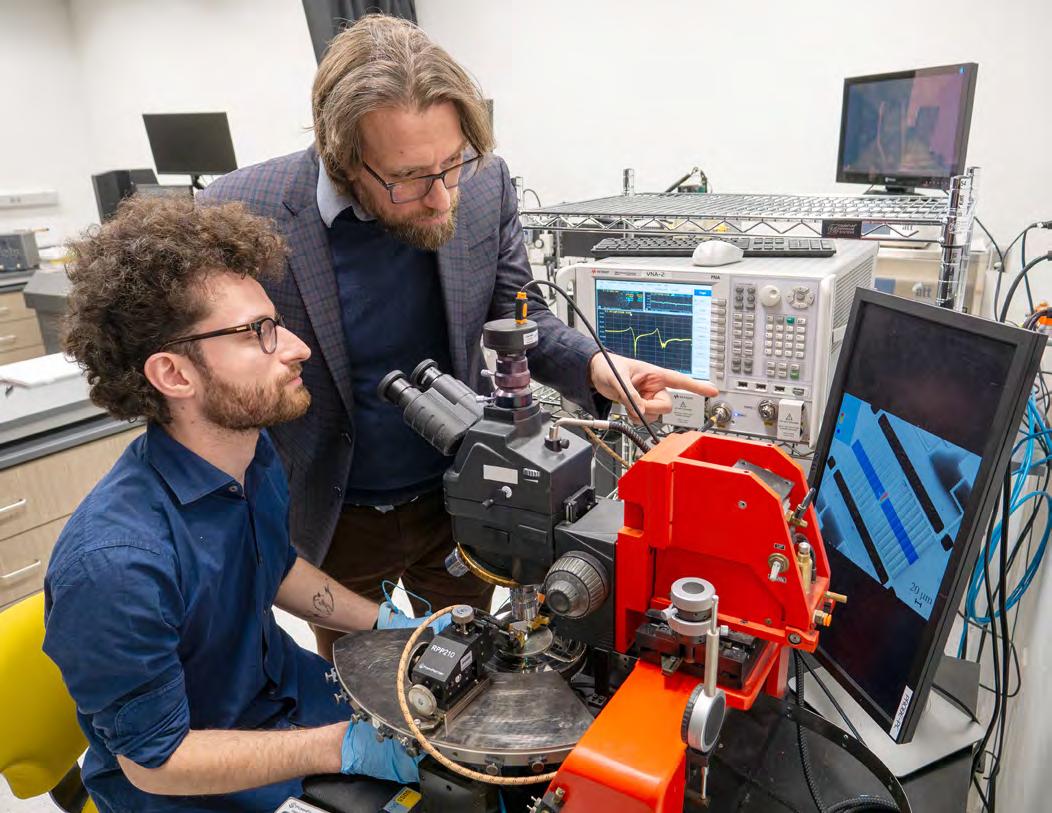
“By relying on the concepts of elastic metamaterials at the microscale, we will show for the first time that we can create a mode of vibration that cannot be found in nature with superior gyroscopic properties. This could be the missing puzzle piece needed to ensure positioning and navigation in GPS-denied environments.”
Cristian
Cassella
associate professor of electrical and computer engineering
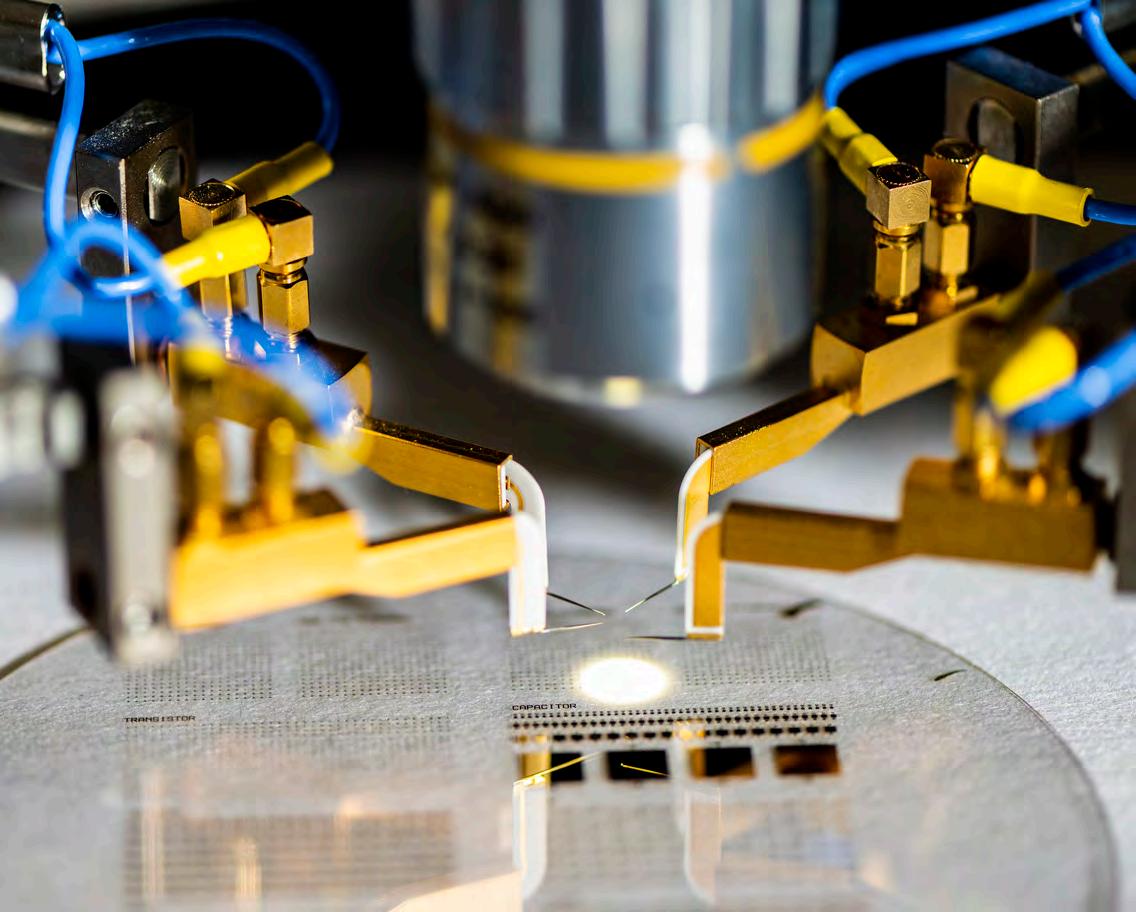
The current microelectronics manufacturing method is expensive, slow, and energy and resource intensive. But Ahmed Busnaina, university distinguished and William Lincoln Smith professor of mechanical and industrial engineering, has patented a new process and printer that manufacturers electronics and chips more efficiently, at reduced cost, and at nanoscale.
“I thought that there must be an easier way to do this, there must be a cheaper way to do this,” says Busnaina. “We started, basically, with very simple physical chemistry with a very simple approach.”
He explains that the conventional method of microelectronics fabrication basically works by depositing a material in a film and then “etching away” the excess. Each layer presents one part of the circuit and, after many layers build up, a microprocessor or a memory chip is created. For each material used, a different process is used.
But this process has several drawbacks. First, it is expensive. Facilities to fabricate the advanced electronics and chips needed to power today’s electronics cost about $20 billion to $40 billion to build and then $1 billion to operate annually. The expense of the manufacturing facilities—or “fabs”—means that the number of companies capable of building the necessary chips has gone from about 29 at the
beginning of the millennium, to five as of 2018. This translates into a six-month to a one-year timeline to get a chip made, and any revisions after testing requires a similar timeline. Moreover, a typical fab requires an amount of power equivalent to 50,000 homes, because of the need for a vacuum and high temperatures in the manufacturing process.
In contrast, Busnaina developed an additive, “bottom up” manufacturing process at Northeastern’s Innovation Campus in Burlington, Massachusetts, for silicon microprocessor or memory chips that lower the manufacturing cost of electronics to roughly 1% of the current method.
Analogous to sculpting something out of clay rather than sculpting something out of stone, Busnaina explains that you build up, rather than chip away. “We don’t remove anything,” he says. “We only deposit the material we need at the location we need it.” Materials can also be deposited in a very fast process using very small particles, enabling one to create very small objects at a fraction of the time of traditional nanofabrication or 3D printing.
“We showed that we can do structures down to 25 nanometers in one minute, for example, over a large area,” Busnaina says. “So it’s high throughput, very low cost.” Busnaina’s process is also estimated to reduce the carbon footprint by 10 to 20 times compared to conventional fabrication, depending on the assembly process used.
He predicts that the new method and tool could “democratize” the process of chip manufacturing. “It’s like the old Kinkos—where you’d go and you make your own copies,” Busnaina says. “Now you can go to a 3D printing shop and give them your chip design, and they’ll make it for you the same day or the next day.”
“Imagine if every chip designer can actually have the chance to get their design in the same week and then do development and then scale it up,” Busnaina continues. “You will not only democratize the nanomanufacturing of electronics, you will accelerate the pace of innovation in electronics and make all electronics very affordable.” N
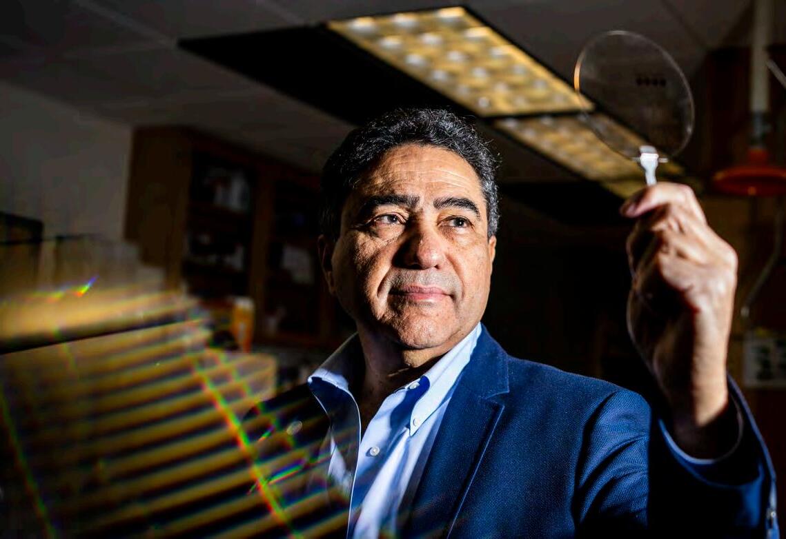
Ahmed Busnaina, university distinguished and William Lincoln Smith professor of mechanical and industrial engineering, has patented a process and printer that manufacturers electronics and chips more efficiently, at reduced cost, and at nanoscale.
Optical chips are increasingly critical for high-speed processing. They are used in an array of technologies such as optical communications, imaging, sensors, augmented and virtual reality displays, solar energy harvesting, and quantum computing.
Advancing the design of optical chips can substantially expand their applications, while reducing costs, increasing computing speed and capacity, and saving energy.
With combined funding of nearly $2 million from the National Science Foundation, Yongmin Liu, professor of mechanical and industrial engineering, and electrical and computer engineering, is researching two approaches to bring optical chips mainstream. One effort is developing engineered photonic materials to build optical chips, while the other focuses on designing a new optical processing architecture based on artificial neural networks.
At the heart of optical chips are photonic materials made from naturally occurring elements like crystals. By engineering the composition and/or underlying physical structure of the photonic materials in optical chips, through a process typically involving numerical simulation, nanofabrication, and optical characterization, it is possible to dramatically enhance the optical responses and performance of the way they generate, process, or detect light. The traditional approach to doing this, however, relies on time-consuming trial-and-error, and case-by-case explorations.
“Fundamentally, we want to create optical properties not existing in nature,” says Liu, who is collaborating with Sunil Mittal, assistant professor of electrical and computer engineering, and researchers at Purdue University and the Georgia Institute of Technology.
By using artificial materials, the team is creating designs at a nanoscale level, which would not be possible with naturally occurring materials. At nanoscale, photonic materials can be designed with only the tiniest of a variance, so each would have a different outcome in how it controls light.
“We are engineering the optical properties to have different responses to light,” Liu says. “Small particles can scatter and even block light, but we can design them to guide light through the system.”
Additionally, the use of artificial intelligence (AI) provides significant advantages over current modeling and simulation techniques. Because of the vast amount of data and variables needed to map new nanostructures for photonic materials, current simulation approaches could take days or even weeks. The horsepower of AI not only shortens that process, but it can also draw from a much wider range of possibilities for designing photonic structures.
“We could completely replace the electronic devices in computers with all-optical chips. The benefit is that we can achieve extremely high-speed processing, operating at the speed of light, while consuming much less power.”
Yongmin Liu professor of mechanical and industrial engineering, and electrical and computer engineering
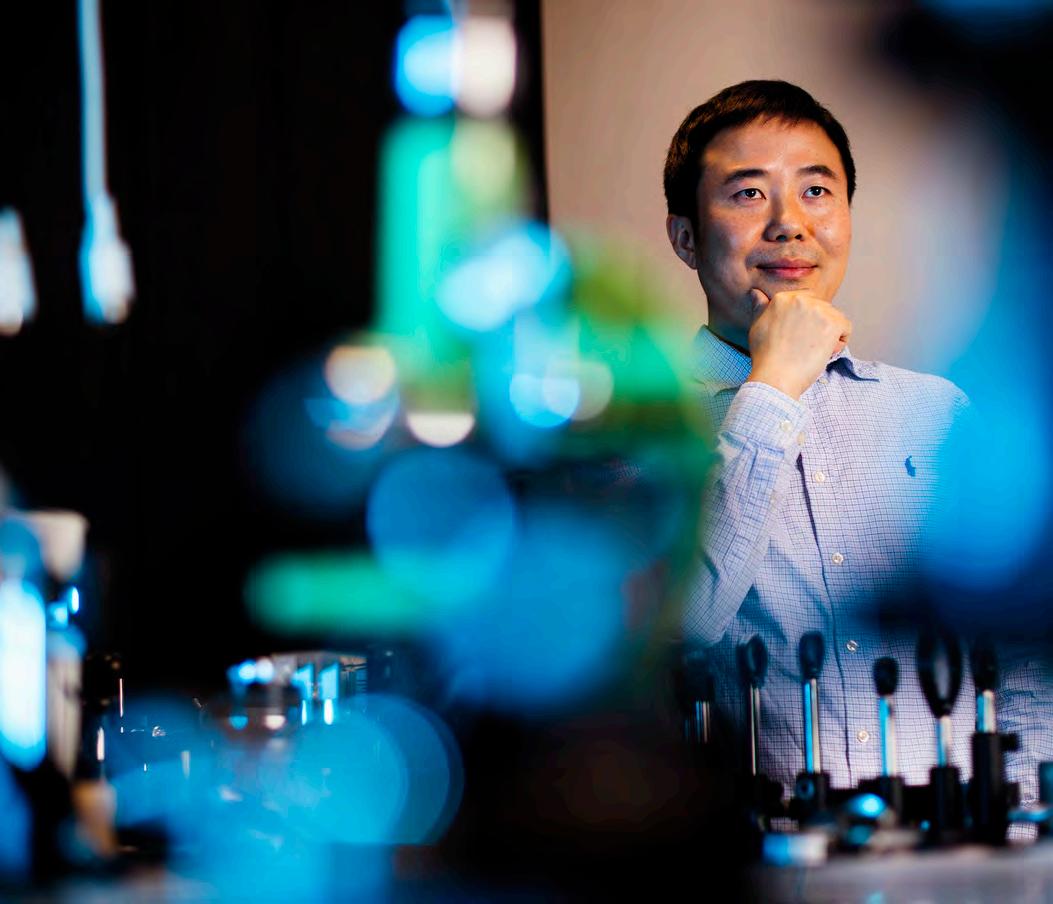
Liu is also adapting the principles of artificial neural networks for optical computing. He is designing an optical chip architecture in which multiple nodes can simultaneously process data to achieve far faster results than conventional computing models that rely on electronic components.
“We could completely replace the electronic devices in computers,” Liu says. “The benefit is that we can achieve extremely high-speed processing, operating at the speed of light, while consuming much less power.”
The neural-network design focuses on a metasurface-based structure that has layers of optical processing components. Each component has many neurons, which are artificially engineered and smaller than the wavelength of light, measured in nanometers. The layers of neurons cascade onto each other, transmitting their data or computations to other neurons that need information to perform their own functions. Together they form a network, or web of neurons, passing light that carries data through the system.
“We are building single layer metasurfaces and then we want to stack them together,” Liu says. “The overall size will be very small, about 100-by-100 micrometers in the three-dimensional format, which is comparable to a single human hair.” N
Quantum computing holds the promise of processing data, solving complex problems, and creating simulations and modeling beyond the capabilities of any conventional supercomputer today. However, these computers are powered by qubit processors, which are fragile and easily destabilized, leading to processing errors. To help keep them stable, they require very cool temperature environments and supporting electronics, which leads to high costs and the need for large spaces to accommodate the equipment.
Compact semiconductor-scale components for quantum computers would enable less expensive and more scalable computers for widespread deployment.
Supported by a CAREER Award from the National Science Foundation, Aravind Nagulu, assistant professor of electrical and computer engineering, is developing compact components for quantum computers that would reduce their size to semiconductor scale, enabling less expensive and more scalable computers. “With this research, the technology could be accessible without a huge upfront investment,” Nagulu says.
He is designing cryogenic complementary metal-oxidesemiconductor (CMOS) versions of the electronics a quantum computer uses to support the qubit processors and manage functions like communications. Conventional electronics are built onto room-temperature racks that sit adjacent to a quantum computer. Depending on the complexity of the system, the racks can cost in the $100,000 range to upwards of $1 million and require considerable physical space. The proposed approach would enable supporting electronics to be reduced to semiconductor-size—a fraction of the size they are today.
“We want to compact the rack into tiny CMOS integrated circuits, so the cost of a quantum computer is reduced dramatically,” Nagulu says.
The design calls for semiconductor components that can function at very low temperature levels. Qubits operate in cold temperatures, which helps to mute noise and vibrations. “If the noise is high, quantum computers cannot do the things that we are aiming to do with them. The idea is to bring those electronics into the cool temperature environment so that the electronics will generate less noise and can be tightly integrated with the qubits,” Nagulu says.
“We want to compact the rack into tiny CMOS integrated circuits, so the cost of a quantum computer is reduced dramatically.”
Aravind Nagulu assistant professor of electrical and computer engineering

Furthermore, to increase the scalability of superconducting quantum computers, Nagulu is developing superconducting circuits that can sit on the same semiconductor as the qubit. Currently, quantum computers use components called circulators and isolators to help protect the qubit from external noise. They can each measure several inches in size and a single qubit processor may need up to a half dozen of them.
Nagulu is developing a time-modulation component that emulates the tasks of conventional circulators and isolators. “It has been very difficult to integrate current technology because of material and fabrication limitations,” he says. By integrating the time-modulation-based circulators onto the qubit processor, the need for separate off-chip circulators and isolators can be eliminated.
“Right now, quantum computers are deployed primarily by big companies and they’re working on very important problems,” Nagulu says. “But there are many applications for quantum computers that can be explored in smaller environments as well. This research could enable the widespread deployment of quantum computing.” N
When stationed in dangerous, rural areas, the last thing soldiers should worry about is replacing a dead battery. That’s one reason why in 2017 the Defense Advanced Research Projects Agency awarded Matteo Rinaldi, professor of electrical and computer engineering, a grant to develop devices that use virtually no power at all.

Rinaldi, who is also director of the Institute for NanoSystems Innovation, and his research team, designed a new type of sensor that consumes no power in standby mode. When the sensor recognizes a specific infrared wavelength signature, it uses the tiny amount of power contained in the infrared radiation to wake itself, significantly extending battery life for years.
The discovery, which addresses a key challenge posed by the internet of things revolution on how to power and maintain the rapidly increasing connected devices worldwide, was published in Nature Nanotechnology, titled “Zero-Power Infrared Digitizers Based on Plasmonically Enhanced Micromechanical Photoswitches.” Since then, this zero-power sensor technology has been patented and applied to many other applications. With funding from the Bill & Melinda Gates Foundation, Rinaldi and his team developed a sensor for monitoring agricultural crop health. When plants are infected by a disease, struggling to find water, or attacked by pests, they produce volatile organic chemicals. Those chemicals are used to trigger a chemical reaction in the sensor, which acts like a switch, turning on a circuit to connect the system to an otherwise unused battery. The device can then use battery power to wirelessly broadcast a signal to alert the farmer that there is a problem.
“When the chemical is not present, the sensor will consume absolutely zero power,” says Zhenyun Qian, associate research professor of electrical and computer engineering.
“Only when the chemical is released by the plant it is near will the device be activated. Since the device doesn’t require power until it is activated, it can remain on standby until the end of the battery’s natural lifetime, which could be as long as a decade.”

In the same agriculture sector, the technology was transformed into a low-power crop water stress sensor that exploits the sunlight transmitted through a plant leaf in the short-wave infrared spectral band for longterm monitoring of water stress and sensor-automated irrigation. This research was supported by the Advanced Research Projects Agency-Energy.
In addition, with a grant from the National Science Foundation, the same concept was used to develop a flame sensor for fire monitoring. This time, the sensor was designed to selectively harvest energy from specific infrared signatures that hydrocarbon flames release, and use it to activate a wireless transmitter to communicate the time and the location of the detected fire accident. Numerous other applications are also possible. More recently, the technology is being applied to people presence detection for smart home, building automation, and security applications with research and development funding supported by the Department of Homeland Security and Northeastern University. N
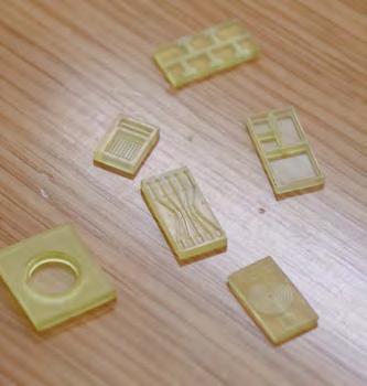
Students in Assistant Professor Benyamin Davaji’s Biomedical Microsystems class developed microfluidic chip designs for their chosen applications as part of a semester-long biochip tape-out project. The microfluidic chips were manufactured for the class by Boston Micro Fabrication according to students’ specifications, providing valuable insight into the feasibility, advantages, and drawbacks of the designs. When presenting their designs, students discussed the specific applications they studied, such as microfluidic tactile sensors for use in minimally invasive surgical techniques, cell mechanobiology for direct stiffness measurements, and terahertz spectroscopy for biomolecular imaging.
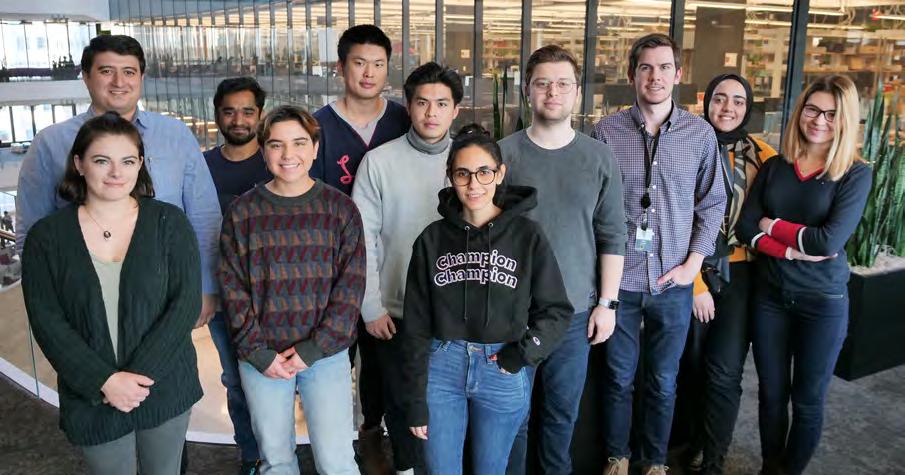
With over 240 tenured/tenure-track faculty and 20 multidisciplinary research centers and institutes with funding by eight federal agencies, the College of Engineering is a leader in experiential education and interdisciplinary research with a focus on innovating to address global challenges for societal impact. Northeastern’s global university system—with engineering programs on campuses across the U.S. and in multiple countries—provides flexible academic offerings, innovative partnerships, and the ability to scale ideas, talent, and solutions.
Founded in 1898, Northeastern is a global research university and the recognized leader in experiential lifelong learning. Our approach of integrating real-world experience with education, research, and innovation empowers our students, faculty, alumni, and partners to create worldwide impact.
Northeastern’s personalized, experiential undergraduate and graduate programs lead to degrees through the doctorate in 10 colleges and schools across our 13 campuses worldwide. Learning emphasizes the intersection of data, technology, and human literacies, uniquely preparing graduates for careers of the future and lives of fulfillment and accomplishment.
Our research enterprise, with an R1 Carnegie classification, is solutions oriented and spans the world. Our faculty scholars and students work in teams that cross not just disciplines, but also sectors— aligned around solving today’s highly interconnected global challenges and focused on transformative impact for humankind.
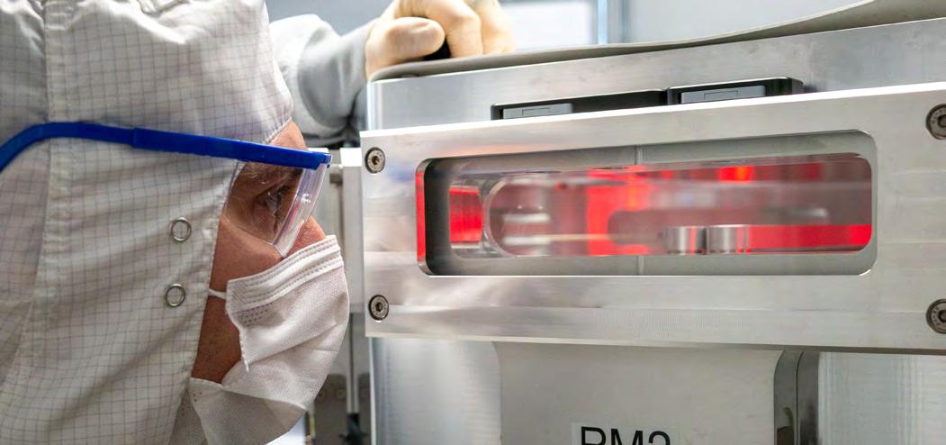
The Institute for NanoSystems Innovation at Northeastern University is located at campuses on the East and West coasts. In addition to many unique experimental capabilities, a clean room is available on the Boston campus, with a 20,000 sq. ft. clean room planned at the Innovation Campus in Burlington, Massachusetts. Shown is a researcher piloting manufacturing of high-performance piezoelectric micro and nano systems. See page 2.
