3 minute read
APPLICATIONS

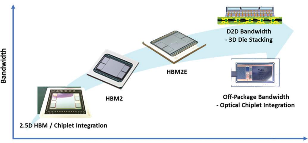
ASIC and four HBMs are integrated on a silicon interposer using micro-bumps. The interposer is then assembled on a 70X70mm organic substrate.
Recent advances and ongoing developments in hybrid bonding (combined metal and dielectric bond) provide another step function improvement in interconnect density (Figure 13). Hybrid bonding is the ideal candidate to achieve 10 μm and submicron scale for connectivity as compared to 100 µm pitch in advanced flip-chip technology. Both die-to-wafer (D2W) and D2D hybrid solutions address reticle size limitations for manufacturing large dies. The reduction in pitch provides flexibility in SoC portioning. Furthermore, reduction of interconnection lengths from mm length to micron length, along with high area interconnect densities enabled by finer pitches, enables a true 3D structure with reduced footprint, low latency and high bandwidth while increasing the total SoC area. In addition to packaging portioned SoC dies, hybrid bonding enables stacking of 3D dynamic random access memory (DRAM), heterogeneous integra- tion at high I/O densities, lower power consumption, and form factor reduction.
Cpo
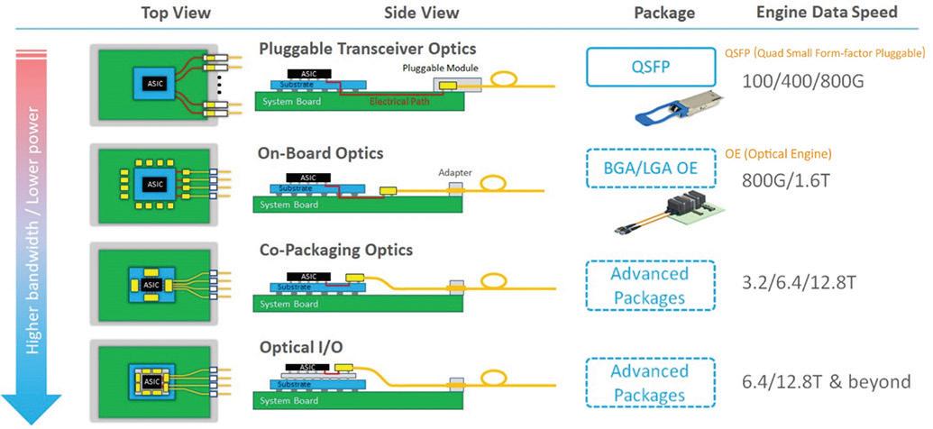
What is beyond the traditional copper transmission lines? This becomes clearer when considering the speed a signal can travel through copper vs the speed of light. The next level of performance packaging for long-distance signal transmission is moving from the traditional copper conductor lines to light-based lines. Silicon photonics has been around since the mid-90s, but has faced technical and cost challenges. Since then, technical improvements and power-hungry scaling bandwidth requirements have driven the industry to accelerate the adoption of silicon photonics. Advances in module-based packaging of both pre-packaged and nonpackaged components have helped in the evolution toward CPO. When we look at the various ways network switches can be organized, there is a clear reason why co-packaging the switch die and optics are key. Figure 14 shows the increasing insertion loss (lower performance) and higher power requirements depending on how the communication is handled between the transmit and receive functions of the backplane.
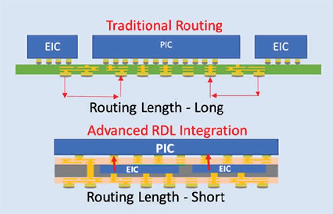
This co-package configuration improvement reduces the losses between transmission lines and should follow similar rules when looking at IC packaging methodology. Looking at CPO closer, we see that this more integrated packaging methodology is bringing the critical components closer together to minimize losses between the electro-optical conversion process. Because of the custom nature of photonics ICs CPO generally does not follow any pre-defined packaging rules, which lead to many different types of configurations within the industry. To further improve the CPO area, components must be integrated in the most efficient way while keeping in mind the best way to attach the optical fiber. As mentioned above, when components are placed in a 2D plane, there are longer lines and losses associated with the layout. This can be further enhanced by creative packaging as shown in Figure 15. This figure shows a traditional PIC die next to the EIC, sideby side approach, but a more efficient structure is shown by vertical coupling or grading coupling where the EIC die are located directly below the photonic IC. This is enabled by utilizing a double-sided fan-out wafer-level package structure that embeds two driver EIC die right below the photonic IC die, thereby minimizing the critical length between the dies. This type of sub-module integration can help to enable another level of performance improvement for CPO.
Summary
The industry continues to evolve and the new challenges are requiring new solutions. Six critically important packaging technologies form the pillars of ASE’s VIPack™ platform and are supported by a comprehensive and integrated co-design ecosystem. As described in this article, these pillars include ASE’s high-density RDL-based FOPoP, FOCoS, FOCoSBridge, and FOSiP, as well as TSV-based 2.5D and 3D IC and CPO processing capabilities. The VIPack™ platform provides the capabilities necessary to enable highly-integrated silicon packaging solutions required to optimize clock speed, bandwidth, and power delivery, and to reduce co-design time, product development, and time to market.
These six pillars will help to deliver unique opportunities to those seeking optimum efficiency and performance for their applications. The technology pillars are built upon an open silicon ecosystem in partnership with foundries, component suppliers, and across the supply chain to provide design flexibility required for product realization. A spectrum of new process tools further enhances ASE’s current toolbox of capabilities and supports evolving package structures being developed in alignment with industry roadmaps. ◆
Authors
The ASE authors are based in North America and include members of the global engineering, marketing, and technical promotion team: Mark Gerber, Dr. Lihong Cao, Dr. Vikas Gupta, and Patricia MacLeod. Please contact Mark Gerber with any comments or questions: mark. gerber@aseus.com


