Principles of Electronic Materials and Devices 4th Edition Safa O. Kasap
Visit to download the full and correct content document: https://ebookmass.com/product/principles-of-electronic-materials-and-devices-4th-edit ion-safa-o-kasap/


Fourth Edition PRINCIPLES OF Electronic Materials & Devices S. O. KASAP
PRINCIPLES OF ELECTRONIC MATERIALS AND DEVICES
PRINCIPLES OF ELECTRONIC MATERIALS AND DEVICES
FOURTH EDITION
S. O. Kasap
University of Saskatchewan Canada
PRINCIPLES OF ELECTRONIC MATERIALS AND DEVICES, FOURTH EDITION
Published by McGraw-Hill Education, 2 Penn Plaza, New York, NY 10121. Copyright © 2018 by McGraw-Hill Education. All rights reserved. Printed in the United States of America. Previous editions © 2006, 2002, 2000 (revised first edition), and 1997. No part of this publication may be reproduced or distributed in any form or by any means, or stored in a database or retrieval system, without the prior written consent of McGraw-Hill Education, including, but not limited to, in any network or other electronic storage or transmission, or broadcast for distance learning.
Some ancillaries, including electronic and print components, may not be available to customers outside the United States.
This book is printed on acid-free paper.
1 2 3 4 5 6 7 8 9 LCR 21 20 19 18 17
ISBN 978-0-07-802818-2
MHID 0-07-802818-3
Chief Product Officer, SVP Products & Markets: G. Scott Virkler
Vice President, General Manager, Products & Markets: Marty Lange
Vice President, Content Design & Delivery: Betsy Whalen
Managing Director: Ryan Blankenship
Brand Manager: Raghothaman Srinivasan/Thomas
M. Scaife, Ph.D.
Director, Product Development: Rose Koos
Product Developer: Tina Bower
Marketing Manager: Shannon O’Donnell
Director, Content Design & Delivery: Linda Avenarius
Program Manager: Lora Neyens
Content Project Managers: Jane Mohr and Sandra Schnee
Buyer: Jennifer Pickel
Design: Studio Montage, St. Louis, MO
Content Licensing Specialist: Lori Hancock
Cover Image: (International Space Station): Source: STS-108 Crew, NASA; (detector structure): Courtesy of Max Planck Institute for Physics; (silicon chip): © Andrew Dunn/Alamy Stock
Photo RF.
Compositor: Aptara®, Inc
Printer: LSC Communications
All credits appearing on page or at the end of the book are considered to be an extension of the copyright page.
LibraryofCongressCataloging-in-PublicationData
Names: Kasap, S. O. (Safa O.), author.
Title: Principles of electronic materials and devices / S. O. Kasap, University of Saskatchewan Canada.
Description: Fourth edition. | New York, NY : McGraw-Hill, a business unit of The McGraw-Hill Companies, Inc., [2018] | Includes bibliographical references and index.
Identifiers: LCCN 2016052438| ISBN 9780078028182 (alk. paper) | ISBN 0078028183 (alk. paper)
Subjects: LCSH: Electrical engineering—Materials. | Electronic apparatus and appliances. | Electric apparatus and appliances.
Classification: LCC TK453 .K26 2018 | DDC 621.382—dc23 LC record available at https://lccn.loc.gov/2016052438
The Internet addresses listed in the text were accurate at the time of publication. The inclusion of a website does not indicate an endorsement by the authors or McGraw-Hill Education, and McGraw-Hill Education does not guarantee the accuracy of the information presented at these sites.
mheducation.com/highered
BRIEF CONTENTS
Chapter 1
Elementary Materials Science Concepts 3
Chapter 2
ElectricalandThermalConductionin Solids:MainlyClassicalConcepts
Chapter 3
Elementary Quantum Physics
Chapter 4
Modern Theory of Solids
Chapter 5 Semiconductors
Chapter 6
Chapter 7
Chapter 8
Magnetic Properties and Superconductivity
Chapter 9
Appendix
Appendix
Appendix
Appendix
Index
v
125
213
313
411
Semiconductor
527
Devices
DielectricMaterialsandInsulation 659
767
859
Optical Properties of Materials
Law and
941
A Bragg’s Diffraction
X-ray Diffraction
B MajorSymbolsandAbbreviations 946
C Elements to
953
Uranium
D ConstantsandUsefulInformation 956
961
Table 978
Periodic
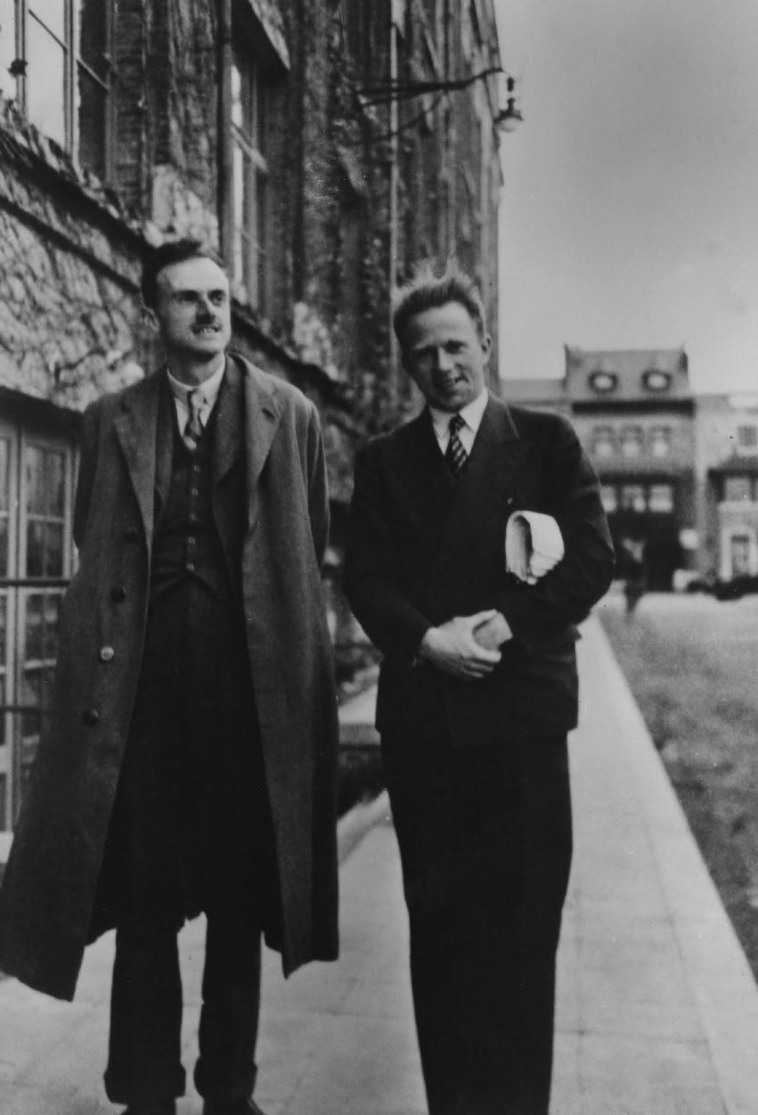
Paul Dirac (1902–1984) and Werner Heisenberg (1901–1976) walking outdoors in Cambridge circa 1930. They received the Nobel Prize in Physics in 1928 and 1932, respectively.
Courtesy of AIP Emilio Segre Visual Archives, Physics Today Collection

Max Planck (1858–1947), a German theoretical physicist, was one of the originators of quantum theory, and won the Nobel Prize in Physics in 1918. His Nobel citation is “in recognition of the services he rendered to the advancement of Physics by his discovery of energy quanta”.
© Alpha Historica/Alamy Stock Photo
vii
Preface xiii Chapter 1 Elementary Materials Science Concepts 3 1.1 Atomic Structure and Atomic Number 3 1.2 Atomic Mass and Mole 8 1.3 Bonding and Types of Solids 9 1.3.1 MoleculesandGeneralBonding Principles 9 1.3.2 CovalentlyBondedSolids: Diamond 11 1.3.3 MetallicBonding:Copper 13 1.3.4 IonicallyBondedSolids:Salt 14 1.3.5 SecondaryBonding 18 1.3.6 MixedBonding 22 1.4 Kinetic Molecular Theory 25 1.4.1 MeanKineticEnergyand Temperature 25 1.4.2 ThermalExpansion 32 1.5 Molecular Velocity and Energy Distribution 37 1.6 Molecular Collisions and Vacuum Deposition 41 1.7 Heat, Thermal Fluctuations, and Noise 45 1.8 Thermally Activated Processes 50 1.8.1 ArrheniusRateEquation 50 1.8.2 AtomicDiffusionandtheDiffusion Coefficient 52 1.9 The Crystalline State 55 1.9.1 TypesofCrystals 55 1.9.2 CrystalDirectionsandPlanes 61 1.9.3 AllotropyandCarbon 66 1.10 Crystalline Defects and Their Significance 69 1.10.1 PointDefects:Vacanciesand Impurities 69 1.10.2 LineDefects:EdgeandScrew Dislocations 73 1.10.3 PlanarDefects:GrainBoundaries 77 1.10.4 CrystalSurfacesandSurface Properties 79 1.10.5 Stoichiometry,Nonstoichiometry,and DefectStructures 82 1.11 Single-Crystal Czochralski Growth 82 1.12 Glasses and Amorphous Semiconductors 85 1.12.1 GlassesandAmorphousSolids 85 1.12.2 CrystallineandAmorphous Silicon 88 1.13 Solid Solutions and Two-Phase Solids 90 1.13.1 IsomorphousSolidSolutions: IsomorphousAlloys 90 1.13.2 PhaseDiagrams:Cu–NiandOther IsomorphousAlloys 91 1.13.3 ZoneRefiningandPureSilicon Crystals 95 1.13.4 BinaryEutecticPhaseDiagramsand Pb–SnSolders 97 Additional Topics 102 1.14 Bravais Lattices 102 1.15 Grüneisen’s Rule 105 Defining Terms 107 Questions and Problems 111 Chapter 2 Electrical and Thermal Conduction in Solids: Mainly Classical Concepts 125 2.1 Classical Theory: The Drude Model 126 2.2 Temperature Dependence of Resistivity: Ideal Pure Metals 134 2.3 Matthiessen’s and Nordheim’s Rules 137 2.3.1 Matthiessen’sRuleandtheTemperature CoefficientofResistivity(α) 137
CONTENTS
viii CONTENTS 2.3.2 SolidSolutionsandNordheim’s Rule 145 2.4 Resistivity of Mixtures and Porous Materials 152 2.4.1 HeterogeneousMixtures 152 2.4.2 Two-PhaseAlloy(Ag–Ni)Resistivity andElectricalContacts 156 2.5 The Hall Effect and Hall Devices 157 2.6 Thermal Conduction 162 2.6.1 ThermalConductivity 162 2.6.2 ThermalResistance 166 2.7 Electrical Conductivity of Nonmetals 167 2.7.1 Semiconductors 168 2.7.2 IonicCrystalsandGlasses 172 Additional Topics 177 2.8 Skin Effect: HF Resistance of a Conductor 177 2.9 AC Conductivity σac 180 2.10 Thin Metal Films 184 2.10.1 ConductioninThinMetalFilms 184 2.10.2 ResistivityofThinFilms 184 2.11 Interconnects in Microelectronics 190 2.12 Electromigration and Black’s Equation 194 Defining Terms 196 Questions and Problems 198 Chapter 3 Elementary Quantum Physics 213 3.1 PHOTONS 213 3.1.1 LightasaWave 213 3.1.2 ThePhotoelectricEffect 216 3.1.3 ComptonScattering 221 3.1.4 BlackBodyRadiation 224 3.2 The Electron as a Wave 227 3.2.1 DeBroglieRelationship 227 3.2.2 Time-IndependentSchrÖdinger Equation 231 3.3 Infinite Potential Well: A Confined Electron 235 3.4 Heisenberg’s Uncertainty Principle 241 3.5 Confined Electron in a Finite Potential Energy Well 244 3.6 Tunneling Phenomenon: Quantum Leak 248 3.7 Potential Box: Three Quantum Numbers 254 3.8 Hydrogenic Atom 257 3.8.1 ElectronWavefunctions 257 3.8.2 QuantizedElectronEnergy 262 3.8.3 OrbitalAngularMomentumand SpaceQuantization 266 3.8.4 ElectronSpinandIntrinsicAngular MomentumS 271 3.8.5 MagneticDipoleMomentofthe Electron 273 3.8.6 TotalAngularMomentumJ 277 3.9 The Helium Atom and the Periodic Table 278 3.9.1 HeAtomandPauliExclusion Principle 278 3.9.2 Hund’sRule 281 3.10 Stimulated Emission and Lasers 283 3.10.1 StimulatedEmissionandPhoton Amplification 283 3.10.2 Helium–NeonLaser 287 3.10.3 LaserOutputSpectrum 290 Additional Topics 292 3.11 Optical Fiber Amplifiers 292 Defining Terms 294 Questions and Problems 298 Chapter 4 Modern Theory of Solids 313 4.1 Hydrogen Molecule: Molecular Orbital Theory of Bonding 313 4.2 Band Theory of Solids 319 4.2.1 EnergyBandFormation 319 4.2.2 PropertiesofElectronsina Band 325 4.3 Semiconductors 328 4.4 Electron Effective Mass 334 4.5 Density of States in an Energy Band 336 4.6 Statistics: Collections of Particles 343 4.6.1 BoltzmannClassicalStatistics 343 4.6.2 Fermi–DiracStatistics 344
CONTENTS ix 4.7 Quantum Theory of Metals 346 4.7.1 FreeElectronModel 346 4.7.2 ConductioninMetals 349 4.8 Fermi Energy Significance 352 4.8.1 Metal–MetalContacts:Contact Potential 352 4.8.2 TheSeebeckEffectandthe Thermocouple 355 4.9 Thermionic Emission and Vacuum Tube Devices 364 4.9.1 ThermionicEmission:Richardson–DushmanEquation 364 4.9.2 SchottkyEffectandField Emission 368 4.10 Phonons 374 4.10.1 HarmonicOscillatorandLattice Waves 374 4.10.2 DebyeHeatCapacity 379 4.10.3 ThermalConductivityof Nonmetals 384 4.10.4 ElectricalConductivity 387 Additional topics 388 4.11 Band Theory of Metals: Electron Diffraction in Crystals 388 Defining Terms 397 Questions and Problems 399 Chapter 5 Semiconductors 411 5.1 Intrinsic Semiconductors 412 5.1.1 SiliconCrystalandEnergyBand Diagram 412 5.1.2 ElectronsandHoles 413 5.1.3 ConductioninSemiconductors 416 5.1.4 ElectronandHoleConcentrations 418 5.2 Extrinsic Semiconductors 426 5.2.1 n-TypeDoping 427 5.2.2 p-TypeDoping 429 5.2.3 CompensationDoping 430 5.3 Temperature Dependence of Conductivity 435 5.3.1 CarrierConcentrationTemperature Dependence 435 5.3.2 DriftMobility:Temperatureand ImpurityDependence 440 5.3.3 ConductivityTemperature Dependence 443 5.3.4 DegenerateandNondegenerate Semiconductors 445 5.4 Direct and Indirect Recombination 447 5.5 Minority Carrier Lifetime 451 5.6 Diffusion and Conduction Equations, and Random Motion 457 5.7 Continuity Equation 463 5.7.1 Time-DependentContinuity Equation 463 5.7.2 Steady-StateContinuityEquation 465 5.8 Optical Absorption 469 5.9 Piezoresistivity 473 5.10 Schottky Junction 477 5.10.1 SchottkyDiode 477 5.10.2 SchottkyJunctionSolarCelland Photodiode 482 5.11 Ohmic Contacts and Thermoelectric Coolers 487 Additional Topics 492
Seebeck Effect in Semiconductors and Voltage Drift 492
Direct and Indirect Bandgap Semiconductors 495 5.14 Indirect Recombination 505 5.15 Amorphous Semiconductors 505 Defining Terms 508 Questions and Problems 511 Chapter 6 Semiconductor Devices 527 6.1 Ideal pn Junction 528 6.1.1 NoAppliedBias:OpenCircuit 528 6.1.2 ForwardBias:Diffusion Current 533 6.1.3 ForwardBias:Recombinationand TotalCurrent 539 6.1.4 ReverseBias 541 6.2 pn Junction Band Diagram 548 6.2.1 OpenCircuit 548 6.2.2 ForwardandReverseBias 550 6.3 Depletion Layer Capacitance of the pn Junction 553
5.12
5.13
x CONTENTS 6.4 Diffusion (Storage) Capacitance and Dynamic Resistance 559 6.5 Reverse Breakdown: Avalanche and Zener Breakdown 562 6.5.1 AvalancheBreakdown 562 6.5.2 ZenerBreakdown 564 6.6 Light Emitting Diodes (LED) 566 6.6.1 LEDPrinciples 566 6.6.2 HeterojunctionHigh-Intensity LEDs 568 6.6.3 QuantumWellHighIntensity LEDs 569 6.7 Led Materials and Structures 572 6.8 Led Output Spectrum 576 6.9 Brightness and Efficiency of LEDs 582 6.10 Solar Cells 586 6.10.1 PhotovoltaicDevicePrinciples 586 6.10.2 SeriesandShuntResistance 593 6.10.3 SolarCellMaterials,Devices,and Efficiencies 595 6.11 Bipolar Transistor (BJT) 598 6.11.1 CommonBase(CB) DC Characteristics 598 6.11.2 CommonBaseAmplifier 607 6.11.3 CommonEmitter(CE) DC Characteristics 609 6.11.4 Low-FrequencySmall-Signal Model 611 6.12 Junction Field Effect Transistor (JFET) 614 6.12.1 GeneralPrinciples 614 6.12.2 JFETAmplifier 620 6.13 Metal-Oxide-Semiconductor Field Effect Transistor (MOSFET) 624 6.13.1 FieldEffectandInversion 624 6.13.2 EnhancementMOSFET 626 6.13.3 ThresholdVoltage 631 6.13.4 IonImplantedMOSTransistorsand Poly-SiGates 633 Additional Topics 635 6.14 pin Diodes, Photodiodes, and Solar Cells 635 6.15 Semiconductor Optical Amplifiers and Lasers 638 Defining Terms 641 Questions and Problems 645 Chapter 7 Dielectric Materials and Insulation 659 7.1 Matter Polarization and Relative Permittivity 660 7.1.1 RelativePermittivity:Definition 660 7.1.2 DipoleMomentandElectronic Polarization 661 7.1.3 PolarizationVectorP 665 7.1.4 LocalField Eloc andClausius–MossottiEquation 669 7.2 Electronic Polarization: Covalent Solids 671 7.3 Polarization Mechanisms 673 7.3.1 IonicPolarization 673 7.3.2 Orientational(Dipolar) Polarization 674 7.3.3 InterfacialPolarization 676 7.3.4 TotalPolarization 678 7.4 Frequency Dependence: Dielectric Constant and Dielectric Loss 679 7.4.1 DielectricLoss 679 7.4.2 DebyeEquations,Cole–Cole Plots,andEquivalentSeries Circuit 688 7.5 Gauss’s Law and Boundary Conditions 691 7.6 Dielectric Strength and Insulation Breakdown 696 7.6.1 DielectricStrength:Definition 696 7.6.2 DielectricBreakdownandPartial Discharges:Gases 697 7.6.3 DielectricBreakdown:Liquids 700 7.6.4 DielectricBreakdown:Solids 701 7.7 Capacitor Dielectric Materials 710 7.7.1 TypicalCapacitorConstructions 710 7.7.2 Dielectrics:Comparison 715 7.8 Piezoelectricity, Ferroelectricity, and Pyroelectricity 719 7.8.1 Piezoelectricity 719 7.8.2 Piezoelectricity:QuartzOscillators andFilters 724 7.8.3 FerroelectricandPyroelectric Crystals 727
CONTENTS xi Additional Topics 734 7.9 Electric Displacement and Depolarization Field 734 7.10 Local Field and the Lorentz Equation 738 7.11 Dipolar Polarization 740 7.12 Ionic Polarization and Dielectric Resonance 742 7.13 Dielectric Mixtures and Heterogeneous Media 747 Defining Terms 750 Questions and Problems 753 Chapter 8 Magnetic Properties and Superconductivity 767 8.1 Magnetization of Matter 768 8.1.1 MagneticDipoleMoment 768 8.1.2 AtomicMagneticMoments 769 8.1.3 MagnetizationVectorM 770 8.1.4 MagnetizingFieldorMagneticField IntensityH 773 8.1.5 MagneticPermeabilityandMagnetic Susceptibility 774 8.2 Magnetic Material Classifications 778 8.2.1 Diamagnetism 778 8.2.2 Paramagnetism 780 8.2.3 Ferromagnetism 781 8.2.4 Antiferromagnetism 781 8.2.5 Ferrimagnetism 782 8.3 Ferromagnetism Origin and the Exchange Interaction 782 8.4 Saturation Magnetization and Curie Temperature 785 8.5 Magnetic Domains: Ferromagnetic Materials 787 8.5.1 MagneticDomains 787 8.5.2 MagnetocrystallineAnisotropy 789 8.5.3 DomainWalls 790 8.5.4 Magnetostriction 793 8.5.5 DomainWallMotion 794 8.5.6 PolycrystallineMaterialsandthe M versus H Behavior 795 8.5.7 Demagnetization 799 8.6 Soft and Hard Magnetic Materials 801 8.6.1 Definitions 801 8.6.2 InitialandMaximum Permeability 802 8.7 Soft Magnetic Materials: Examples and Uses 803 8.8 Hard Magnetic Materials: Examples and Uses 806 8.9 Energy Band Diagrams and Magnetism 812 8.9.1 PauliSpinParamagnetism 812 8.9.2 EnergyBandModelof Ferromagnetism 814 8.10 Anisotropic and Giant Magnetoresistance 815 8.11 Magnetic Recording Materials 820 8.11.1 GeneralPrinciplesofMagnetic Recording 820 8.11.2 MaterialsforMagneticStorage 825 8.12 Superconductivity 829 8.12.1 ZeroResistanceandtheMeissner Effect 829 8.12.2 TypeIandTypeII Superconductors 832 8.12.3 CriticalCurrentDensity 834 8.13 Superconductivity Origin 838 Additional Topics 840 8.14 Josephson Effect 840 8.15 Flux Quantization 842 Defining Terms 843 Questions and Problems 847 Chapter 9 Optical Properties of Materials 859 9.1 Light Waves in a Homogeneous Medium 860 9.2 Refractive Index 863 9.3 Dispersion: Refractive Index–Wavelength Behavior 865 9.4 Group Velocity and Group Index 870 9.5 Magnetic Field: Irradiance and Poynting Vector 873 9.6 Snell’s Law and Total Internal Reflection (TIR) 875 9.7 Fresnel’s Equations 879 9.7.1 AmplitudeReflectionandTransmission Coefficients 879

Left: Circular bright rings make up the diffraction pattern obtained when an electron beam is passed through a thin polycrystalline aluminum sheet. The pattern results from the wave behavior of the electrons; the waves are diffracted by the Al crystals. Right: A magnet brought to the screen bends the electron paths and distorts the diffraction pattern. The magnet would have no effect if the pattern was due to X-rays, which are electromagnetic waves. Courtesy of Farley Chicilo
xii CONTENTS 9.7.2 Intensity,Reflectance,and Transmittance 885 9.8 Complex Refractive Index and Light Absorption 890 9.9 Lattice Absorption 898 9.10 Band-To-Band Absorption 900 9.11 Light Scattering in Materials 903 9.12 Attenuation in Optical Fibers 904 9.13 Luminescence, Phosphors, and White Leds 907 9.14 Polarization 912 9.15 Optical Anisotropy 914 9.15.1 UniaxialCrystalsandFresnel’s OpticalIndicatrix 915 9.15.2 BirefringenceofCalcite 919 9.15.3 Dichroism 920 9.16 Birefringent Retarding Plates 920 9.17 Optical Activity and Circular Birefringence 922 9.18 Liquid Crystal Displays (LCDs) 924 9.19 Electro-Optic Effects 928 Defining Terms 932 Questions and Problems 935
Diffraction Law and X-ray Diffraction 941
947
Appendix A Bragg’s
Appendix B MajorSymbolsandAbbreviations
Elements to Uranium 955
959 Index 961
Table 978
Appendix C
Appendix D ConstantsandUsefulInformation
Periodic
PREFACE
FOURTH EDITION
The textbook represents a first course in electronic materials and devices for undergraduate students. With the additional topics, the text can also be used in a graduate-level introductory course in electronic materials for electrical engineers and material scientists. The fourth edition is an extensively revised and extended version of the third edition based on reviewer comments and the developments in electronic and optoelectronic materials over the last ten years. The fourth edition has many new and expanded topics, new worked examples, new illustrations, and new homework problems. The majority of the illustrations have been greatly improved to make them clearer. A very large number of new homework problemshavebeenadded,andmanymoresolved problems have been provided that put the concepts into applications. More than 50% of the illustrations have gone through some kind of revision to improve the clarity. Furthermore, more terms have been added under Defining Terms, which the students have found very useful. Bragg’s diffraction law that is mentioned in several chapters is kept as Appendix A for those readers who are unfamiliar with it.
The fourth edition is one of the few books on the market that have a broad coverage of electronic materials that today’s scientists and engineers need. I believe that the revisions have improved the rigor without sacrificing the original semiquantitative approach that both the studentsandinstructorsliked.Themajorrevisionsin scientific content can be summarized as follows:
Chapter 1 Thermal expansion; kinetic molecular theory; atomic diffusion; molecular collisions and vacuum deposition; particle flux density;
line defects; planar defects; crystal surfaces; Grüneisen’s rule.
Chapter 2 Temperature dependence of resistivity, strain gauges, Hall effect; ionic conduction; Einstein relation for drift mobility and diffusion; ac conductivity; resistivity of thin films; interconnects in microelectronics; electromigration.
Chapter 3 Electron as a wave; infinite potential well; confined electron in a finite potential energy well; stimulated emission and photon amplification; He–Ne laser, optical fiber amplification.
Chapter 4 Work function; electron photoemission; secondary emission; electron affinity and photomultiplication; Fermi–Dirac statistics; conduction in metals; thermoelectricity and Seebeck coefficient; thermocouples; phonon concentration changes with temperature.
Chapter 5 Degenerate semiconductors; direct and indirect recombination; E vs. k diagrams for direct and indirect bandgap semiconductors; Schottky junction and depletion layer; Seebeck effect in semiconductors and voltage drift.
Chapter 6 The pn junction; direct bandgap pn junction; depletion layer capacitance; linearly graded junction; hyperabrupt junctions; light emitting diodes (LEDs); quantum well high intensity LEDs; LED materials and structures; LED characteristics; LED spectrum; brightness
xiii
and efficiency of LEDs; multijunction solar cells.
Chapter 7 Atomic polarizability; interfacial polarization; impact ionization in gases and breakdown; supercapacitors.
Chapter 8 anisotropic and giant magnetoresistance; magnetic recording materials; longitudinal and vertical magnetic recording; materials for magnetic storage; superconductivity.
Chapter 9 Refractive and group index of Si; dielectric mirrors; free carrier absorption; liquid crystal displays.
ORGANIZATION AND FEATURES
In preparing the fourth edition, as in previous edition, I tried to keep the general treatment and various proofs at a semiquantitative level without goingintodetailedphysics.Manyoftheproblems have been set to satisfy engineering accreditation requirements. Some chapters in the text have additional topics to allow a more detailed treatment, usually including quantum mechanics or more mathematics. Cross referencing has been avoided as much as possible without too much repetition and to allow various sections and chapters to be skipped as desired by the reader. The text has been written so as to be easily usable in onesemester courses by allowing such flexibility. Some important features are:
∙ The principles are developed with the minimum of mathematics and with the emphasis onphysicalideas.Quantummechanicsispart of the course but without its difficult mathematical formalism.
∙ There are numerous worked examples or solved problems, most of which have a practical significance. Students learn by way of examples, however simple, and to that end a large number (227 in total) of solved problems have been provided.
∙ Even simple concepts have examples to aid learning.
∙ Most students would like to have clear diagramstohelpthemvisualizetheexplanations and understand concepts. The text includes 565 illustrations that have been professionally prepared to reflect the concepts and aid the explanations in the text. There are also numerous photographs of practical devices and scientists and engineers to enhance the learning experience.
∙ The end-of-chapter questions and problems (346 in total) are graded so that they start with easy concepts and eventually lead to more sophisticated concepts. Difficult problems are identified with an asterisk (*). Many practical applications with diagrams have been included.
∙ There is a glossary, Defining Terms, at the end of each chapter that defines some of the concepts and terms used, not only within the text but also in the problems.
∙ The end of each chapter includes a section Additional Topics to further develop important concepts,tointroduceinterestingapplications, or to prove a theorem. These topics are intended for the keen student and can be used as part of the text for a two-semester course.
∙ The text is supported by McGraw-Hill’s textbook website that contains resources, such as solved problems, for both students and instructors.
∙ The fourth edition is supported by an extensive PowerPoint presentation for instructors who have adopted the book for their course. The PowerPoint has all the illustrations in color, and includes additional color photos. The basic concepts and equations are also highlighted in additional slides.
∙ There is a regularly updated online extended Solutions Manual for all instructors; simply locate the McGraw-Hill website for this textbook. The Solutions Manual provides not only detailed explanations to the solutions, but also has color diagrams as well as
xiv PREFACE
references and helpful notes for instructors. (It also has the answers to those “why?” questions in the text.)
ACKNOWLEDGMENTS
My gratitude goes to my past and present graduate students and postdoctoral research fellows, who have kept me on my toes and read various sections of this book. I have been fortunate to have a colleague and friend like Charbel Tannous (Brest University) who, as usual, made many sharply criticalbuthelpfulcomments,especiallyonChapter 8. My best friend and colleague of many years Robert Johanson (University of Saskatchewan), with whom I share teaching this course, also provided a number of critical comments towards the fourth edition. A number of reviewers, at various times, read various portions of the manuscript and provided extensive comments. A number of instructors also wrote to me with their own comments. I incorporated the majority of the suggestions, which I believe made this a better book. No textbook is perfect, and I’m sure that there will be more suggestions (and corrections) for the next edition. I’d like to personally thank them all for their invaluable critiques.
I’d like to thank Tina Bower, my present Product Developer, and Raghu Srinivasan, my
former Global Brand Manager, at McGraw-Hill Education for their continued help throughout the writing and production of this edition. They were always enthusiastic, encouraging, forgiving (everytimeImissedadeadline)andalwaysfinding solutions. It has been a truly great experience working with MHE since 1993. I’m grateful to Julie De Adder (Photo Affairs) who most diligently obtained the permissions for the thirdparty photos in the fourth edition without missing any. The copyright fees (exuberant in many cases) have been duly paid and photos from this book or its PowerPoint should not be copied into other publications without contacting the original copyright holder. If you are an instructor and like the book, and would like to see a fifth edition, perhaps a color version, the best way to make your comments and suggestions heard is not to write to me but to write directly to the Electrical Engineering Editor, McGraw-Hill Education, 501 Bell St., Dubuque, IA 52001, USA. Both instructors and students are welcome to email me with their comments. While I cannot reply to each email, I do read all my emails and take note; it was those comments that led to a major content revision in this edition.
Safa Kasap
Saskatoon, March, 2017
“The important thing in science is not so much to obtain new facts as to discover new ways of thinking about them.”
Sir William Lawrence Bragg
To Nicolette
PREFACE 1


 Left: GaAs ingots and wafers. GaAs is a III–V compound semiconductor because Ga and As are from Groups III and V, respectively.
Right: An InxGa1 xAs (a III–V compound semiconductor)-based photodetector.
Left: Courtesy of Sumitomo Electric Industries. Right: Courtesy of Thorlabs.
Left: A detector structure that will be used to detect dark matter particles. Each individual cylindrical detector has a CaWO4 single crystal, similar to that shown on the bottom right. These crystals are called scintillators, and convert high-energy radiation to light. The Czochralski technique is used to grow the crystal shown on top right, which is a CaWO4 ingot. The detector crystal is cut from this ingot.
Left: Courtesy of Max Planck Institute for Physics. Right: Reproduced from Andreas Erb and Jean-Come Lanfranchi, CrystEngCom, 15, 2301, 2015, by permission of the Royal Society of Chemistry. All rights reserved.
Left: GaAs ingots and wafers. GaAs is a III–V compound semiconductor because Ga and As are from Groups III and V, respectively.
Right: An InxGa1 xAs (a III–V compound semiconductor)-based photodetector.
Left: Courtesy of Sumitomo Electric Industries. Right: Courtesy of Thorlabs.
Left: A detector structure that will be used to detect dark matter particles. Each individual cylindrical detector has a CaWO4 single crystal, similar to that shown on the bottom right. These crystals are called scintillators, and convert high-energy radiation to light. The Czochralski technique is used to grow the crystal shown on top right, which is a CaWO4 ingot. The detector crystal is cut from this ingot.
Left: Courtesy of Max Planck Institute for Physics. Right: Reproduced from Andreas Erb and Jean-Come Lanfranchi, CrystEngCom, 15, 2301, 2015, by permission of the Royal Society of Chemistry. All rights reserved.
Elementary Materials Science Concepts1
Understanding the basic building blocks of matter has been one of the most intriguing endeavors of humankind. Our understanding of interatomic interactions has now reached a point where we can quite comfortably explain the macroscopic properties of matter, based on quantum mechanics and electrostatic interactions between electrons and ionic nuclei in the material. There are many properties of materials that can be explained by a classical treatment of the subject. In this chapter, as well as in Chapter 2, we treat the interactions in a material from a classical perspective and introduce a number of elementary concepts. These concepts do not invoke any quantum mechanics, which is a subject of modern physics and is introduced in Chapter 3. Although many useful engineering properties of materials can be treated with hardly any quantum mechanics, it is impossible to develop the science of electronic materials and devices without modern physics.
1.1 ATOMIC STRUCTURE AND ATOMIC NUMBER
The model of the atom that we must use to understand the atom’s general behavior involves quantum mechanics, a topic we will study in detail in Chapter 3. For the present, we will simply accept the following facts about a simplified, but intuitively satisfactory, atomic model called the shell model, based on the Bohr model (1913).
The mass of the atom is concentrated at the nucleus, which contains protons and neutrons. Protons are positively charged particles, whereas neutrons are neutral particles, and both have about the same mass. Although there is a Coulombic repulsion 1
3 CHAPTER
This chapter may be skipped by readers who have already been exposed to an elementary course in materials science.
subshells
between the protons, all the protons and neutrons are held together in the nucleus by the strong force, which is a powerful, fundamental, natural force between particles. This force has a very short range of influence, typically less than 10−15 m. When the protons and neutrons are brought together very closely, the strong force overcomes the electrostatic repulsion between the protons and keeps the nucleus intact. The number of protons in the nucleus is the atomic number Z of the element.
The electrons are assumed to be orbiting the nucleus at very large distances compared to the size of the nucleus. There are as many orbiting electrons as there are protons in the nucleus. An important assumption in the Bohr model is that only certain orbits with fixed radii are stable around the nucleus. For example, the closest orbit of the electron in the hydrogen atom can only have a radius of 0.053 nm. Since the electron is constantly moving around an orbit with a given radius, over a long time period (perhaps ∼10−12 seconds on the atomic time scale), the electron would appear as a spherical negative-charge cloud around the nucleus and not as a single dot representing a finite particle. We can therefore view the electron as a charge contained within a spherical shell of a given radius.
Due to the requirement of stable orbits, the electrons therefore do not randomly occupy the whole region around the nucleus. Instead, they occupy various welldefined spherical regions. They are distributed in various shells and subshells within the shells, obeying certain occupation (or seating) rules.2 The example for the carbon atom is shown in Figure 1.1.
The shells and subshells that define the whereabouts of the electrons are labeled using two sets of integers, n and ℓ. These integers are called the principal and orbital angular momentum quantum numbers, respectively. (The meanings of these names are not critical at this point.) The integers n and ℓ have the values n = 1, 2, 3, . . . , and ℓ = 0, 1, 2, . . . , n − 1, and ℓ < n. For each choice of n, there are n values of ℓ, so higher-order shells contain more subshells. The shells corresponding to n = 1, 2, 3, 4, . . . are labeled by the capital letters K, L, M, N, . . . , and the subshells denoted by ℓ = 0, 1, 2, 3, . . . are labeled s, p, d, f . . . . The
2 In Chapter 3, in which we discuss the quantum mechanical model of the atom, we will see that these shells and subshells are spatial regions around the nucleus where the electrons are most likely to be found.
4 CHAPTER 1 ∙ ELEMENTARY MATERIALS SCIENCE CONCEPTS
2
1s K
Nucleus
s 2p
L L shell with two
1s22s22p2 or [He]2s22p2
Figure 1.1 The shell model of the carbon atom, in which the electrons are confined to certain shells and subshells within shells.
Maximum
subshell with ℓ = 1 in the n = 2 shell is thus labeled the 2p subshell, based on the standard notation nℓ.
There is a definite rule to filling up the subshells with electrons; we cannot simply put all the electrons in one subshell. The number of electrons a given subshell can take is fixed by nature to be3 2(2ℓ + 1). For the s subshell (ℓ = 0), there are two electrons, whereas for the p subshell, there are six electrons, and so on. Table 1.1 summarizes the most number of electrons that can be put into various subshells and shells of an atom. Obviously, the larger the shell, the more electrons it can take, simply because it contains more subshells. The shells and subshells are filled starting with those closest to the nucleus as explained next.
The number of electrons in a subshell is indicated by a superscript on the subshell symbol, so the electronic structure, or configuration, of the carbon atom (atomic number 6) shown in Figure 1.1 becomes 1s 22s 22p 2. The K shell has only one subshell, which is full with two electrons. This is the structure of the inert element He. We can therefore write the electronic configuration more simply as [He]2s 22p 2. The general rule is to put the nearest previous inert element, in this case He, in square brackets and write the subshells thereafter.
The electrons occupying the outer subshells are the farthest away from the nucleus and have the most important role in atomic interactions, as in chemical reactions, because these electrons are the first to interact with outer electrons on neighboring atoms. The outermost electrons are called valence electrons and they determine the valency of the atom. Figure 1.1 shows that carbon has four valence electrons in the L shell.
When a subshell is full of electrons, it cannot accept any more electrons and it is said to have acquired a stable configuration. This is the case with the inert elements at the right-hand side of the Periodic Table, all of which have completely filled subshells and are rarely involved in chemical reactions. The majority of such elements are gases inasmuch as the atoms do not bond together easily to form a liquid or solid. They are sometimes used to provide an inert atmosphere instead of air for certain reactive materials.
3 We will actually show this in Chapter 3 using quantum mechanics.
1.1 ATOMIC STRUCTURE AND ATOMIC NUMBER 5
Table 1.1
ℓ =0 1 2 3 n Shell s p d f 1 K 2 2 L 2 6 3 M 2 6 10 4 N 2 6 10 14
possible number of electrons in the shells and subshells of an atom
Subshell
Virial theorem
In an atom such as the Li atom, there are two electrons in the 1s subshell and one electron in the 2s subshell. The atomic structure of Li is 1s 22s 1. The third electron is in the 2s subshell, rather than any other subshell, because this is the arrangement of the electrons that results in the lowest overall energy for the whole atom. It requires energy (work) to take the third electron from the 2s to the 2p or higher subshells as will be shown in Chapter 3. Normally the zero energy reference corresponds to the electron being at infinity, that is, isolated from the atom. When the electron is inside the atom, its energy is negative, which is due to the attraction of the positive nucleus. An electron that is closer to the nucleus has a lower energy. The electrons nearer the nucleus are more closely bound and have higher binding energies. The 1s 22s 1 configuration of electrons corresponds to the lowest energy structure for Li and, at the same time, obeys the occupation rules for the subshells. If the 2s electron is somehow excited to another outer subshell, the energy of the atom increases, and the atom is said to be excited.
The smallest energy required to remove a single electron from a neutral atom and thereby create a positive ion (cation) and an isolated electron is defined as the ionization energy of the atom. The Na atom has only a single valence electron in its outer shell, which is the easiest to remove. The energy required to remove this electron is 5.1 electron volts (eV), which is the Na atom’s ionization energy. The electron affinity represents the energy that is needed, or released, when we add an electron to a neutral atom to create a negative ion (anion). Notice that the ionization term implies the generation of a positive ion, whereas the electron affinity implies that we have created a negative ion. Certain atoms, notably the halogens (such as F, Cl, Br, and I), can actually attract an electron to form a negative ion. Their electron affinities are negative. When we place an electron into a Cl atom, we find that an energy of 3.6 eV is released. The Cl ion has a lower energy than the Cl atom, which means that it is energetically favorable to form a Cl ion by introducing an electron into the Cl atom.
There is a very useful theorem in physics, called the Virial theorem, that allows us to relate the average kinetic energy KE, average potential energy PE, and average total or overall energy E of an electron in an atom, or electrons and nuclei in a molecule, through two remarkably simple relationships,4
E = KE + PE and KE =− 1 2 PE [1.1]
For example, if we define zero energy for the H atom as the H+ ion and the electron infinitely separated, then the energy of the electron in the H atom is −13.6 eV. It takes 13.6 eV to ionize the H atom. The average PE of the electron, due to its Coulombic interaction with the positive nucleus, is −27.2 eV. Its average KE turns out to be 13.6 eV. Example 1.1 uses the Virial theorem to calculate the radius of the hydrogen atom, the velocity of the electron, and its frequency of rotation.
4 While the final result stated in Equation 1.1 is elegantly simple, the actual proof is quite involved and certainly not trivial. As stated here, the Virial theorem applies to a system of charges that interact through electrostatic forces only.
6 CHAPTER 1 ∙ ELEMENTARY MATERIALS SCIENCE CONCEPTS
VIRIAL THEOREM AND THE BOHR ATOM
Consider the hydrogen atom in Figure 1.2 in which the electron is in the stable 1s orbit with a radius ro. The ionization energy of the hydrogen atom is 13.6 eV.
a. It takes 13.6 eV to ionize the hydrogen atom, i.e., to remove the electron to infinity. If the condition when the electron is far removed from the hydrogen nucleus defines the zero reference of energy, then the total energy of the electron within the H atom is −13.6 eV. Calculate the average PE and average KE of the electron.
b. Assume that the electron is in a stable orbit of radius ro around the positive nucleus. What is the Coulombic PE of the electron? Hence, what is the radius ro of the electron orbit?
c. What is the velocity of the electron?
d. What is the frequency of rotation (oscillation) of the electron around the nucleus?
SOLUTION
a. From Equation 1.1 we obtain
E = PE + KE = 1 2 PE
or PE =2E =2×(−13.6 eV)=−27.2 eV
The average kinetic energy is
KE =− 1 2 PE =13.6 eV
b. The Coulombic PE of interaction between two charges Q1 and Q2 separated by a distance ro, from elementary electrostatics, is given by
PE
4
4
4
where we substituted Q1 = −e (electron’s charge), and Q2 = +e (charge of the nucleus). Thus the radius ro is
ro =− (1.6×10⁻¹⁹ C)2
4π(8.85×10⁻¹² F m−1)(−27.2 eV×1.6×10−19 J/eV) =5.29×10⁻¹¹ m or 0.0529 nm
which is called the Bohr radius (also denoted ao).
Stable orbit has radius
r o
v +e
r o
1.1 ATOMIC STRUCTURE AND ATOMIC NUMBER 7
=
1Q2
Q
πεoro = (−e)(+e)
πεoro =− e 2
πεoro
EXAMPLE 1.1
–e
Figure 1.2 The planetary model of the hydrogen atom in which the negatively charged electron orbits the positively charged nucleus.
c. Since KE = 1 2 mev 2, the average velocity is
d. The period of orbital rotation
The
1.2 ATOMIC MASS AND MOLE
We had defined the atomic number Z as the number of protons in the nucleus of an atom. The atomic mass number A is simply the total number of protons and neutrons in the nucleus. It may be thought that we can use the atomic mass number A of an atom to gauge its atomic mass, but this is done slightly differently to account for the existence of different isotopes of an element; isotopes are atoms of a given element that have the same number of protons but a different number of neutrons in the nucleus. The atomic mass unit (amu) u is a convenient atomic mass unit that is equal to 1 12 of the mass of a neutral carbon atom that has a mass number A = 12 (6 protons and 6 neutrons). It has been found that u = 1.66054 × 10⁻²⁷ kg.
The atomic mass or relative atomic mass or simply atomic weight Mat of an element is the average atomic mass, in atomic mass units, of all the naturally occurring isotopes of the element. Atomic masses are listed in the Periodic Table. Avogadro’s number NA is the number of atoms in exactly 12 grams of carbon-12, which is 6.022 × 10²³ to three decimal places. Since the atomic mass Mat is defined as 1 12 of the mass of the carbon-12 atom, it is straightforward to show that NA number of atoms of any substance have a mass equal to the atomic mass Mat in grams.
A mole of a substance is that amount of the substance that contains exactly Avogadro’s number NA of atoms or molecules that make up the substance. One mole of a substance has a mass as much as its atomic (molecular) mass in grams. For example, 1 mole of copper contains 6.022 × 10²³ number of copper atoms and has a mass of 63.55 grams. Thus, an amount of an element that has 6.022 × 10²³ atoms has a mass in grams equal to the atomic mass. This means we can express the atomic mass as grams per unit mole (g mol−1). The atomic mass of Au is 196.97 amu or g mol−1. Thus, a 10 gram bar of gold has (10 g)∕(196.97 g mol−1) or 0.0507 moles.
Frequently we have to convert the composition of a substance from atomic percentage to weight percentage, and vice versa. Compositions in materials engineering generally use weight percentages, whereas chemical formulas are given in terms of atomic composition. Suppose that a substance (an alloy or a compound) is composed of two elements, A and B. Let the weight fractions of A and B be wA and wB, respectively. Let nA and nB be the atomic or molar fractions of A and B; that is, nA represents the fraction of type A atoms, nB represents the fraction of type B atoms
8 CHAPTER 1 ∙ ELEMENTARY MATERIALS SCIENCE CONCEPTS
v = √ KE 1 2 me = √ 13.6 eV×1.6×10−19 J/eV 1 2 (9.1×10⁻³¹ kg) =2.19×10⁶ m s 1
T is T = 2πro v = 2π(0.0529×10⁻⁹ m) 2.19×10⁶ m s −1 =1.52×10⁻¹⁶ seconds
orbital
f = 1∕T = 6.59 × 10¹⁵ s −1 (Hz).
frequency
in the whole substance, and nA + nB = 1. Suppose that the atomic masses of A and B are MA and MB. Then nA and nB are given by
nA =
wA∕MA wA∕M
where wA + wB = 1. Equation 1.2 can be readily rearranged to obtain wA and wB in terms of nA and nB. Weight
COMPOSITIONS IN ATOMIC AND WEIGHT PERCENTAGES Consider a Pb–Sn solder that is 38.1 wt.% Pb and 61.9 wt.% Sn (this is the eutectic composition with the lowest melting point). What are the atomic fractions of Pb and Sn in this solder?
SOLUTION
For Pb, the weight fraction and atomic mass are, respectively, wA = 0.381 and MA = 207.2 g mol−1 and for Sn, wB = 0.619 and MB = 118.71 g mol−1. Thus, Equation 1.2 gives
wA∕MA
nA =
wA∕MA + wB∕MB = (0.381) ∕ (207.2)
0.381∕207.2+0.619∕118.71 =0.261 or 26.1 at.%
wB∕MB
and nB =
wA∕MA +
Thus the alloy is 26.1 at.% Pb and 73.9 at.% Sn, which can be written as Pb0.261 Sn0.739
1.3 BONDING AND TYPES OF SOLIDS
1.3.1 MOLECULES AND GENERAL BONDING PRINCIPLES
When two atoms are brought together, the valence electrons interact with each other and with the neighbor’s positively charged nucleus. The result of this interaction is often the formation of a bond between the two atoms, producing a molecule. The formation of a bond means that the energy of the system of two atoms together must be less than that of the two atoms separated, so that the molecule formation is energetically favorable, that is, more stable. The general principle of molecule formation is illustrated in Figure 1.3a, showing two atoms brought together from infinity. As the two atoms approach each other, the atoms exert attractive and repulsive forces on each other as a result of mutual electrostatic interactions. Initially, the attractive force FA dominates over the repulsive force FR. The net force FN is the sum of the two,
FN = FA + FR
and this is initially attractive, as indicated in Figure 1.3a. Note that we have defined the attractive force as negative and repulsive force as positive in Figure 1.3a.5
5 In some materials science books and in the third edition of this book, the attractive force is shown as positive, which is an arbitrary choice. A positive attractive force is more appealing to our intuition.
EXAMPLE 1.2
1.3 BONDING AND TYPES OF SOLIDS 9
+ w
∕MB and nB =1− nA [1.2]
A
B
to
percentage
force
atomic
Net
wB∕MB = (0.619) ∕ (118.71) 0.381∕207.2+0.619∕118.71 =0.739 or
73.9 at.%
Repulsion Attraction Force
Net force and potential energy
r o
Separated atoms
FR = Repulsive force
FA = Attractive force
FN = Net force
E ( r )
Repulsion Attraction
ER = Repulsive energy
E = Net energy Ebond
(a) Force versus r r r Potential Energy,
EA = Attractive PE
(b) Potential energy versus r
Net force in bonding between atoms
represents attraction.
The potential energy E(r) of the two atoms can be found from6
FN =− dE dr
by integrating the net force
FN. Figure 1.3a and b show the variation of the net force
FN(r) and the overall potential energy E(r) with the interatomic separation r as the two atoms are brought together from infinity. The lowering of energy corresponds to an attractive interaction between the two atoms.
The variations of FA and FR with distance are different. Force FA varies slowly, whereas FR varies strongly with separation and is strongest when the two atoms are very close. When the atoms are so close that the individual electron shells overlap, there is a very strong electron-to-electron shell repulsion and FR dominates. An equilibrium will be reached when the attractive force just balances the repulsive force and the net force is zero, or
FN = FA + FR = 0 [1.3]
In this state of equilibrium, the atoms are separated by a certain distance ro, as shown in Figure 1.3. This distance is called the equilibrium separation and is effectively 0
6 Remember that the change dE in the PE is the work done by the force, dE = −FN dr. In Figure 1.3b, when the atoms are far separated, dE/dr is negative, which represents an attractive force.
10 CHAPTER 1 ∙ ELEMENTARY MATERIALS SCIENCE CONCEPTS
= ∞
r
Molecule
r o r o 0
Figure 1.3 (a) Force versus interatomic separation and (b) potential energy versus interatomic separation. Note that the negative sign
the bond length. On the energy diagram, FN = 0 means dE∕dr = 0, which means that the equilibrium of two atoms corresponds to the potential energy of the system acquiring its minimum value. Consequently, the molecule will only be formed if the energy of the two atoms as they approach each other can attain a minimum. This minimum energy also defines the bond energy of the molecule, as depicted in Figure 1.3b. An energy of Ebond is required to separate the two atoms, and this represents the bond energy.
Although we considered only two atoms, similar arguments also apply to bonding between many atoms, or between billions of atoms as in a typical solid. Although the actual details of FA and FR will change from material to material, the general principle that there is a bonding energy Ebond per atom and an equilibrium interatomic separation ro will still be valid. Even in a solid in the presence of many interacting atoms, we can still identify a general potential energy curve E(r) per atom similar to the type shown in Figure 1.3b. We can also use the curve to understand the properties of the solid, such as the thermal expansion coefficient and elastic and bulk moduli.
1.3.2 COVALENTLY BONDED SOLIDS: DIAMOND
Two atoms can form a bond with each other by sharing some or all of their valence electrons and thereby reducing the overall potential energy of the combination. The covalent bond results from the sharing of valence electrons to complete the subshells of each atom. Figure 1.4 shows the formation of a covalent bond between two hydrogen atoms as they come together to form the H2 molecule. When the 1s subshells overlap, the electrons are shared by both atoms and each atom now has a complete subshell. As illustrated in Figure 1.4, electrons 1 and 2 must now orbit both atoms;
H atomH atom
Covalent bond
H–H molecule
1s Figure 1.4 Formation of a covalent bond between two H atoms, leading to the H2 molecule. Electrons spend a majority of their time between the two nuclei, which results in a net attraction between the electrons and the two nuclei, which is the origin of the covalent bond.
1.3 BONDING AND TYPES OF SOLIDS 11
1s Electron shell
1 1 2 2
2
1
Figure 1.5 (a) Covalent bonding in methane, CH4, which involves four hydrogen
sharing electrons with one carbon atom. Each covalent bond has two shared electrons. The four bonds are identical and repel each other. (b) Schematic sketch of CH4 on paper. (c) In three dimensions, due to symmetry, the bonds are directed toward the corners of a tetrahedron.
they therefore cross the overlap region more frequently, indeed twice as often. Thus, electron sharing, on average, results in a greater concentration of negative charge in the region between the two nuclei, which keeps the two nuclei bonded to each other. Furthermore, by synchronizing their motions, electrons 1 and 2 can avoid crossing the overlap region at the same time. For example, when electron 1 is at the far right (or left), electron 2 is in the overlap region; later, the situation is reversed.
The electronic structure of the carbon atom is [He]2s 22p 2 with four empty seats in the 2p subshell. The 2s and 2p subshells, however, are quite close. When other atoms are in the vicinity, as a result of interatomic interactions, the two subshells become indistinguishable and we can consider only the shell itself, which is the L shell with a capacity of eight electrons. It is clear that the C atom with four vacancies in the L shell can readily share electrons with four H atoms, as depicted in Figure 1.5a and b, whereby the C atom and each of the H atoms attain complete shells. This is the CH4 molecule, which is the gas methane. The repulsion between the electrons in one bond and the electrons in a neighboring bond causes the bonds to spread as far out from each other as possible, so that in three dimensions, the H atoms occupy the corners of an imaginary tetrahedron and the CH bonds are at an angle of 109.5° to each other, as sketched in Figure 1.5c.
The C atom can also share electrons with other C atoms, as shown in Figure 1.6. Each neighboring C atom can share electrons with other C atoms, leading to a threedimensional network of a covalently bonded structure. This is the structure of the precious diamond crystal, in which all the carbon atoms are covalently bonded to each other, as depicted in the figure. The coordination number (CN) is the number of nearest neighbors for a given atom in the solid. As is apparent in Figure 1.6, the coordination number for a carbon atom in the diamond crystal structure is 4.
Due to the strong Coulombic attraction between the shared electrons and the positive nuclei, the covalent bond energy is usually the highest for all bond types,
12 CHAPTER 1 ∙ ELEMENTARY MATERIALS SCIENCE CONCEPTS
H 109.5° C H H H H H H H L shell K shell
bond C C H H H H
bonds
Covalent
Covalent
(a)(b)(c)
atoms
Figure 1.6 The diamond crystal is a covalently bonded network of carbon atoms.
Each carbon atom is bonded covalently to four neighbors, forming a regular three-dimensional pattern of atoms that constitutes the diamond crystal.
leading to very high melting temperatures and very hard solids: diamond is one of the hardest known materials.
Covalently bonded solids are also insoluble in nearly all solvents. The directional nature and strength of the covalent bond also make these materials nonductile (or nonmalleable). Under a strong force, they exhibit brittle fracture. Further, since all the valence electrons are locked in the bonds between the atoms, these electrons are not free to drift in the crystal when an electric field is applied. Consequently, the electrical conductivity of such materials is very poor.
1.3.3 METALLIC BONDING: COPPER
Metal atoms have only a few valence electrons, which are not very difficult to remove. When many metal atoms are brought together to form a solid, these valence electrons are lost from individual atoms and become collectively shared by all the ions. The valence electrons therefore become delocalized and form an electron gas or electron cloud, permeating the space between the ions, as depicted in Figure 1.7. The attraction between the negative charge of this electron gas and the metal ions more than compensates for the energy initially required to remove the valence electrons from the individual atoms. Thus, the bonding in a metal is essentially due to the attraction between the stationary metal ions and the freely wandering electrons between the ions.
The bond is a collective sharing of electrons and is therefore nondirectional. Consequently, the metal ions try to get as close as possible, which leads to close-packed crystal structures with high coordination numbers, compared to covalently bonded solids. In the particular example shown in Figure 1.7, Cu+ ions are packed as closely as possible by the gluing effect of the electrons between the ions, forming a crystal structure called the face-centered cubic (FCC). The FCC crystal structure, as explained later in Section 1.9, has Cu+ ions at the corners of a cube and a Cu+ at the center of each cube-face. (See Figure 1.32.)
1.3 BONDING AND TYPES OF SOLIDS 13
Positive metal ion cores
Free valence electrons forming an electron gas
Figure 1.7 In metallic bonding, the valence electrons from the metal atoms form a “cloud of electrons,” which fills the space between the metal ions and “glues” the ions together through Coulombic attraction between the electron gas and the positive metal ions.
The results of this type of bonding are dramatic. First, the nondirectional nature of the bond means that under an applied force, metal ions are able to move with respect to each other, especially in the presence of certain crystal defects (such as dislocations). Thus, metals tend to be ductile. Most importantly, however, the “free” valence electrons in the electron gas can respond readily to an applied electric field and drift along the force of the field, which is the reason for the high electrical conductivity of metals. Furthermore, if there is a temperature gradient along a metal bar, the free electrons can also contribute to the energy transfer from the hot to the cold regions, since they frequently collide with the metal ions and thereby transfer energy. Metals therefore, typically, also have good thermal conductivities; that is, they easily conduct heat. This is why when you touch your finger to a metal it feels cold because it conducts heat “away” from the finger to the ambient (making the fingertip “feel” cold).
1.3.4 IONICALLY BONDED SOLIDS: SALT
Common table salt, NaCl, is a classic example of a solid in which the atoms are held together by ionic bonding. Ionic bonding is frequently found in materials that normally have a metal and a nonmetal as the constituent elements. Sodium (Na) is an alkaline metal with only one valence electron that can easily be removed to form an Na+ ion with complete subshells. The ion Na+ looks like the inert element Ne, but with a positive charge. Chlorine has five electrons in its 3p subshell and can readily accept one more electron to close this subshell. By taking the electron given up by the Na atom, the Cl atom becomes negatively charged and looks like the inert element Ar with a net negative charge. Transferring the valence electron of Na to Cl thus results in two oppositely charged ions, Na+ and Cl , which are called the cation and anion, respectively, as shown in Figure 1.8. As a result of the Coulombic force, the two ions pull each other until the attractive force is just balanced by the
14 CHAPTER 1 ∙ ELEMENTARY MATERIALS SCIENCE CONCEPTS
Closed K and L shells
Closed K and L shells
repulsive force between the closed electron shells. Initially, energy is needed to remove the electron from the Na atom and transfer it to the Cl atom. However, this is more than compensated for by the energy of Coulombic attraction between the two resulting oppositely charged ions, and the net effect is a lowering of the potential energy of the Na+ and Cl ion pair.
When many Na and Cl atoms are ionized and brought together, the resulting collection of ions is held together by the Coulombic attraction between the Na+ and Cl ions. The solid thus consists of Na+ cations and Cl anions holding each other through the Coulombic force, as depicted in Figure 1.9. The Coulombic force around a charge is nondirectional; also, it can be attractive or repulsive, depending on the polarity of the interacting ions. There are also repulsive Coulombic forces between the Na+ ions themselves and between the Cl ions themselves. For the solid to be stable, each Na+ ion must therefore have Cl ions as nearest neighbors and vice versa so that like-ions are not close to each other.
The ions are in equilibrium and the solid is stable when the net potential energy is minimum, or dE∕dr = 0. Figure 1.10 illustrates the variation of the net potential energy for a pair of ions as the interatomic distance r is reduced from infinity to less than the equilibrium separation, that is, as the ions are brought together from infinity. Zero energy corresponds to separated Na and Cl atoms. Initially, about 1.5 eV is required to transfer the electron from the Na to Cl atom and thereby form Na+ and Cl ions. Then, as the ions come together, the energy is lowered, until it reaches a minimum at about 6.3 eV below the energy of the separated Na and Cl atoms. When r = 0.28 nm, the energy is minimum and the
1.3 BONDING AND TYPES OF SOLIDS 15
Cl 3p 3s
Na 3s
Cl–Na+ r o (c) Cl–3p 3s Na+ FA r FA (b)
(a)
Figure 1.8 The formation of an ionic bond between Na and Cl atoms in NaCl. The attraction is due to Coulombic forces.
any
ions are in equilibrium. The bonding energy per ion in solid NaCl is thus 6.3∕2 or 3.15 eV, as is apparent in Figure 1.10. The energy required to take solid NaCl apart into individual Na and Cl atoms is the atomic cohesive energy of the solid, which is 3.15 eV per atom.
In solid NaCl, the Na+ and Cl ions are thus arranged with each one having oppositely charged ions as its neighbors, to attain a minimum of potential energy. Since there is a size difference between the ions and since we must avoid like-ions
16 CHAPTER 1 ∙ ELEMENTARY MATERIALS SCIENCE CONCEPTS Cl– Na+ 6 –6 0 –6.3 0.28 nm Potential energy E(r), eV/(ion-pair) Separation, r Cohesive energy 1.5 eV r = ∞ r = ∞ Cl Na Na+ Cl–r o = 0.28 nm
Cl– Na+ Na+ Na+ Cl– Cl–Cl– Na+ Na+ Na+ Cl– Cl–Cl– Na+ Na+ Na+ Cl– Cl–Cl– Na+ Na+ Na+ Cl– Cl–Cl– Na+ Na+ Na+ Cl– Cl–Cl– Na+ Na+ Na+ Cl– Cl–
Figure 1.10 Sketch of the potential energy per ion pair in solid NaCl.
Zero
energy corresponds to neutral Na and Cl atoms infinitely separated.
(a)(b)
Figure 1.9 (a) A schematic illustration of a cross section from solid NaCl. Solid NaCl is made of Cl and Na+ ions arranged alternatingly, so the oppositely charged ions are closest to each other and attract each other. There are also repulsive forces between the like-ions. In equilibrium, the net force acting on
ion is zero. (b) Solid NaCl.
getting close to each other, if we want to achieve a stable structure, each ion can have only six oppositely charged ions as nearest neighbors. Figure 1.9b shows the packing of Na+ and Cl ions in the solid. The number of nearest neighbors, that is, the coordination number, for both cations and anions in the NaCl crystal is 6.
A number of solids consisting of metal–nonmetal elements follow the NaCl example and have ionic bonding. They are called ionic crystals and, by virtue of their ionic bonding characteristics, share many physical properties. For example, LiF, MgO (magnesia), CsCl, and ZnS are all ionic crystals. They are strong, brittle materials with high melting temperatures compared to metals. Most become soluble in polar liquids such as water. Since all the electrons are within the rigidly positioned ions, there are no free or loose electrons to wander around in the crystal as in metals. Therefore, ionic solids are typically electrical insulators. Compared to metals and covalently bonded solids, ionically bonded solids have lower thermal conductivity since ions cannot readily pass vibrational kinetic energy to their neighbors.
IONIC BONDING AND LATTICE ENERGY
The potential energy E per Na+–Cl pair within the NaCl crystal depends on the interionic separation r as
where the first term is the attractive and the second term is the repulsive potential energy, and M, B, and m are constants explained in the following. If we were to consider the potential energy PE of one ion pair in isolation from all others, the first term would be a simple Coulombic interaction energy for the Na+–Cl pair, and M would be 1. Within the NaCl crystal, however, a given ion, such as Na+, interacts not only with its nearest six Cl neighbors (Figure 1.9b), but also with its twelve second neighbors (Na+), eight third neighbors (Cl ), and so on, so the total or effective PE has a factor M, called the Madelung constant, that takes into account all these different Coulombic interactions. M depends only on the geometrical arrangement of ions in the crystal, and hence on the particular crystal structure; for the FCC crystal structure, M = 1.748. The Na+–Cl ion pair also has a repulsive PE that is due to the repulsion between the electrons in filled electronic subshells of the ions. If the ions are pushed toward each other, the filled subshells begin to overlap, which results in a strong repulsion. The repulsive PE decays rapidly with distance and can be modeled by a short-range PE of the form B∕r m as in the second term in Equation 1.4 where for Na+–Cl , m = 8 and B = 6.972 × 10−96 J m8. Find the equilibrium separation (ro) of the ions in the crystal and the ionic bonding energy, defined as −E(ro). Given the ionization energy of Na (the energy to remove an electron) is 5.14 eV and the electron affinity of Cl (energy released when an electron is added) is 3.61 eV, calculate the atomic cohesive energy of the NaCl crystal as joules per mole.
SOLUTION
Bonding occurs when the potential energy E(r) is a minimum at r = ro corresponding to the equilibrium separation between the Na+ and Cl ions. We differentiate E(r) and set it to zero at r = ro,
1.3 BONDING AND TYPES OF SOLIDS 17
E(r)=− e 2M 4πεor + B r m [1.4]
dE(r) dr = e
M 4πεor 2 mB r m+1 =0 at r = ro
2
EXAMPLE 1.3
Energy per ion pair in an ionic crystal
Solving for ro,
Equilibrium ionic separation
Minimum PE at bonding
Thus,
ro = [
4πεoBm
e 2M ]
1∕(m−1) [1.5]
ro = [
4π(8.85×10⁻¹² F m−1)(6.972×10−96 J m8)(8)
(1.6×10⁻¹⁹ C)2(1.748) ]
1∕(8−1)
=0.281×10⁻⁹ m or 0.28 nm
The minimum energy Emin per ion pair is E(ro) and can be simplified further by substituting for B in terms of ro:
e 2M
Thus,
Emin =−
Emin =−
4πεoro + B r m o =−
e 2M
4πεoro(1− 1 m) [1.6]
(1.6×10⁻¹⁹ C)2(1.748)
4π(8.85×10⁻¹² Fm−1)(2.81×10⁻¹⁰ m) (1− 1 8)
=−1.256×10⁻¹⁸ J or −7.84 eV
This is the energy with respect to two isolated Na+ and Cl ions. We therefore need 7.84 eV to break up a NaCl crystal into isolated Na+ and Cl ions, which represents the ionic cohesive energy. Some authors call this ionic cohesive energy simply the lattice energy. To take the crystal apart into its neutral atoms, we have to transfer the electron from the Cl ion to the Na+ ion to obtain neutral Na and Cl atoms. It takes 3.61 eV to remove the electron from the Cl ion, but 5.14 eV is released when it is put into the Na+ ion. Thus, we need 7.84 eV + 3.61 eV but get back 5.14 eV.
Bond energy per Na–Cl pair = 7.84 eV + 3.61 eV − 5.14 eV = 6.31 eV
The atomic cohesive energy is 3.1 eV/atom. In terms of joules per mole of NaCl, this is Ecohesive = (6.31 eV)(1.6022 × 10⁻¹⁹ J/eV)(6.022 × 1023 mol−1) = 608 kJ mol−1
1.3.5 SECONDARY BONDING
Covalent, ionic, and metallic bonds between atoms are known as primary bonds. It may be thought that there should be no such bonding between the atoms of the inert elements as they have full shells and therefore cannot accept or lose any electrons, nor share any electrons. However, the fact that a solid phase of argon exists at low temperatures, below −189 °C, means that there must be some bonding mechanism between the Ar atoms. The magnitude of this bond cannot be strong because above −189 °C solid argon melts. Although each water molecule H2O is neutral overall, these molecules nonetheless attract each other to form the liquid state below 100 °C and the solid state below 0 °C. Between all atoms and molecules, there exists a weak type of attraction, the so-called van der Waals–London force, which is due to a net electrostatic attraction between the electron distribution of one atom and the positive nucleus of the other.
In many molecules, the concentrations of negative and positive charges do not coincide. As apparent in the HCl molecule in Figure 1.11a, the electrons spend most
18 CHAPTER 1 ∙ ELEMENTARY MATERIALS SCIENCE CONCEPTS
AB'
(a)(b)(c)
Figure 1.11 (a) A permanently polarized molecule is called an electric dipole moment. (b) Dipoles can attract or repel each other depending on their relative orientations. (c) Suitably oriented dipoles attract each other to form van der Waals bonds.
of their time around the Cl nucleus, so the positive nucleus of the H atom is exposed (H has effectively donated its electron to the Cl atom) and the Cl-region acquires more negative charge than the H-region. An electric dipole moment occurs whenever a negative and a positive charge of equal magnitude are separated by a distance as in the H+–Cl molecule in Figure 1.11a. Such molecules are polar, and depending on their relative orientations, they can attract or repel each other as depicted in Figure 1.11b. Two dipoles arranged head to tail attract each other because the closest separation between charges on A and B is between the negative charge on A and the positive charge on B, and the net result is an electrostatic attraction. The magnitude of the net force between two dipoles A and B, however, does not depend on their separation r as 1∕r 2 because there are both attractions and repulsions between the charges on A and charges on B and the net force is only weakly attractive. (In fact, the net force depends on 1∕r 4.) If the dipoles are arranged head to head or tail to tail, then, by similar arguments, the two dipoles repel each other. Suitably arranged dipoles can attract each other and form van der Waals bonds as illustrated in Figure 1.11c. The energies of such dipole arrangements as in Figure 1.11c are less than that of totally isolated dipoles and therefore encourage “bonding.” Such bonds are weaker than primary bonds and are called secondary bonds.
The water molecule H2O is also polar and has a net dipole moment as shown in Figure 1.12a. The attractions between the positive charges on one molecule and the negative charges on a neighboring molecule lead to van der Waals bonding between the H2O molecules in water as illustrated in Figure 1.12b. When the positive charge of a dipole as in H2O arises from an exposed H nucleus, van der Waals bonding is referred to as hydrogen bonding. In ice, the H2O molecules, again attracted by van der Waals forces, bond to form a regular pattern and hence a crystal structure.
Van der Waals attraction also occurs between neutral atoms and nonpolar molecules. Consider the bonding between Ne atoms at low temperatures. Each has closed (or full) electron shells. The center of mass of the electrons in the closed shells, when averaged over time, coincides with the location of the positive nucleus. At any one instant, however, the center of mass is displaced from the nucleus due to various motions of the individual electrons around the nucleus as depicted in Figure 1.13. In fact, the center of mass of all the electrons fluctuates with time about the nucleus.
1.3 BONDING AND TYPES OF SOLIDS 19
H Cl AB
Figure 1.12 The origin of van der Waals bonding between water molecules.
(a) The H2O molecule is polar and has a net permanent dipole moment.
(b) Attractions between the various dipole moments in water give rise to van der Waals bonding.
Time averaged electron (negative charge) distribution
Closed L shell
Ionic core (nucleus + K shell)
Instantaneous electron (negative charge) distribution fluctuates about the nucleus
van der Waals force
Synchronized fluctuations of the electrons
Consequently, the electron charge distribution is not static around the nucleus but fluctuates asymmetrically, giving rise to an instantaneous dipole moment.
When two Ne atoms, A and B, approach each other, the rapidly fluctuating negative charge distribution on one affects the motion of the negative charge distribution on the other. A lower energy configuration (i.e., attraction) is produced when the fluctuations are synchronized so that the negative charge distribution on A gets closer to the nucleus of the other, B, while the negative distribution on B at that instant stays away from that on A as shown in Figure 1.13. The strongest electrostatic interaction arises from the closest charges that are the displaced electrons in A and the nucleus in B. This means that there will be a net attraction between the two atoms and hence a lowering of the net energy that in turn leads to bonding.
This type of attraction between two atoms is due to induced synchronization of the electronic motions around the nuclei, and we refer to this as induced-dipole–induced-dipole interaction. It is weaker than permanent dipole interactions and at least an order of magnitude less than primary bonding. This is the reason why the inert elements Ne and Ar solidify at temperatures below 25 K (−248 °C) and 84 K (−189 °C). Induced dipole–induced dipole interactions also occur between nonpolar molecules such as H2, I2, CH4, etc. Methane gas (CH4) can be solidified at very low temperatures. Solids in which constituent molecules (or atoms) have been bonded by van der Waals forces are known as molecular solids; ice, solidified CO2 (dry ice), O2, H2, CH4, and solid inert gases are typical examples.
20 CHAPTER 1 ∙ ELEMENTARY MATERIALS SCIENCE CONCEPTS
H O H (a)(b)
A
B
Ne
Figure 1.13 Induced-dipole–induced-dipole interaction and the resulting van der Waals force.
