Contents lists available at ScienceDirect

Contents lists available at ScienceDirect

journal homepage: www.elsevier.com/locate/solmat

Martin C. Eze a, b , Godwin Ugwuanyi a , Meng Li d , Hyginus U. Eze b , Guillermo M. Rodriguez a , Alex Evans a , Victoria G. Rocha a , Zhe Li c, ** , Gao Min a, *
a School of Engineering, Cardiff University, Cardiff, CF24 3AA, United Kingdom b Department of Electronic Engineering, University of Nigeria, Nsukka, 410001, Enugu, Nigeria c School of Engineering and Materials Science, Queen’s Mary University of London, London E1 4NS, United Kingdom d Helmholtz-Zentrum Berlin für Materialien und Energie, Kekul´ estraße5, 12489, Berlin, Germany
Keywords:
Perovskite solar cells
Metal electrode
Organic hole transport layer
Magnetron sputtering
The use of magnetron sputtering for deposition of the metal electrode in perovskite solar cells has been limited because of the damage to the organic hole transport layer by high kinetic energy particles during the sputtering process. In this paper, a systematic investigation into the effect of sputtering power, argon flow rate, sputtering duration, and argon pressure on the performance of the perovskite cells was conducted. The results of this work show that high power conversion efficiency of 18.35% was obtained for solution-processed, air-fabricated perovskite solar cells with Ag contact prepared using magnetron sputtering. The devices also exhibit an excellent short-current density of 22.56 mA/cm2, an open-circuit voltage of 1.10 V and a fill factor of 73.7%. The investigation reveals that sputtering power is the most critical factor that needs to be carefully controlled to minimise the damage to the hole transport layer. This study demonstrates that highly efficient perovskite solar cells can be fabricated using magnetron sputtering if the sputtering parameters are optimised.
Perovskite solar cells (PSCs) have become one of the most promising solar cell technologies due to high absorption coefficient, excellent carrier mobility, high dielectric constant, tuneable bandgap, abundance of the materials and low-cost fabrication processes [1–5]. These outstanding properties have led to extensive research in PSCs which resulted in power conversion efficiency (PCE) enhancement from 3.8% in 2009 [6] through 22.6% in 2018 [7] to 23.32% in 2019 [8]. In 2020, a PCE of 24.82% was reported by Jeong et al. [9] while the National Renewable Energy Laboratory (NREL) published a certified PCE of 26.1% [10]. One of the important factors that influence the performance of PSCs is the metal contact characteristics (morphology and electrical properties), which depend on the deposition procedure and material. Although good PCEs have been reported for devices with metal contact deposited by thermal evaporation [7,11–18] and electron beam (e-beam) [19], magnetron sputtering has the advantages of improved film adhesion, precise deposition parameter control, scalability and
* Corresponding author.
** Corresponding author.
E-mail addresses: zhe.li@qmul.ac.uk (Z. Li), min@cardiff.ac.uk (G. Min).
consequently superior metal contact morphology [19–22]. Despite these benefits, magnetron sputtering is rarely used in PSCs fabrication due to the damaging effect of high kinetic energy particles (metal atoms) on organic hole transport layer (HTL) and perovskite layer [19,20]. The HTL gets damaged when the metal particles strike the molecules in the HTL or dope into the HTL/perovskite layers to form recombination sites [23]. The extent of penetration and the number of metal dopants in HTL/perovskite layers depend on the particle kinetic energy and deposition rate, respectively [20]. At very high kinetic energy, numerous metal particles dope in the perovskite layer, leading to very severe performance degradation. Because of this, only a limited number of attempts were made using the magnetron sputtering to deposit metal contact for PSCs [19,20,23–27]. To date, the majority of these studies focused on the effect of magnetron sputtering of different metal contacts on the performance of PSCs [24–27]. A few studies investigated the dependence of PSC performance on the thickness of metal electrode [26, 27] and also the influence of deposition rate [18]. Furthermore, few authors carried out comparative studies of PSC metal electrode
https://doi.org/10.1016/j.solmat.2021.111185 Received 14 November 2020; Received in revised form 2 May 2021; Accepted 10 May 2021
Availableonline24May2021 0927-0248/©2021ElsevierB.V.Allrightsreserved.
fabrication using thermal evaporation, magnetron sputtering and e-beam techniques [19,20,23]. These studies were done in a controlled laboratory environment (glovebox) and best efficiencies reported were 18.32% and 16.51% for devices with sputtered Au and Ag contacts respectively [20,25]. Notwithstanding these reports, systematic study of the effect of sputtering parameters on PSCs’ performance is still lacking, especially for devices processed in ambient lab environments relevant to real-life manufacturing conditions. In this paper, we investigate the effect of sputtering parameters on the performance of PSCs, which include sputtering power, argon flow rate, sputtering duration, and argon pressure. These parameters are selected for study as they have been reported as the most important sputtering parameters during thin film deposition [21], though the researchers only investigated the impact of these parameters on the properties of sputtered films.
The laser-patterned fluorine-doped tin oxide (FTO, TEC-15) glasses were purchased from Pingdingshan Mingshuo Technology Co. Ltd as the substrate. 2,2′ ,7,7′ -Tetrakis (N, N -di-p -methoxyphenylamino)-9,9′ - spirobifluorene (Spiro-OMETAD, 99.8%) was purchased from Borun New Materials. Dimethyl sulfoxide (DMSO, 99.8%), lead (II) iodide (PbI2, 99.999%), lithium bis(trifluoromethylsulfonyl)imide (Li-TFSI, 98%) and methyl acetate (MA, 99%) were purchased from Alfa Aesar. Methylammonium iodide (MAI, 99%), tris(2-(1H-pyrazol-1-yl)-4-tert-butylpyridine)cobalt(III) tris(bis(trifluoromethylsulfonyl)imide) (FK209, 98%), 4tert-Butylpyridine (TBP, 96%) and tin (II) chloride dihydrate (SnCl2.2H2O, 99.995%) were purchased from Sigma Aldrich. The dimethylformamide (DMF, 99.8%) and chlorobenzene (CB, 99.6%) were purchased from Across Organics. Acetonitrile (99.8%) and ethanol, isopropanol and acetone were purchased from Fisher Scientific, silver (Ag) target (99.99%, 2-inch diameter × 0.125-inch thick) was bought from Kurt J. Lesker Company Ltd while 0.45 μm hydrophilic nylon filter was purchased from Ossila LTD.
FTO glasses (20 mm × 15 mm) were cleaned using Hellmanex (III) solution and rinsed with deionized water, followed by successive cleaning in deionized water, acetone and isopropanol using ultrasonic bath at 50 ◦ C for 10 min. Afterwards, the FTO glasses were dried using argon/nitrogen gas and then, treated with ultraviolet (UV)-ozone cleaner for 10 min. For electron transport layer (ETL) preparation, SnO2 film was deposited on FTO by spin-coating 90 μl of SnCl2.2H2O precursor at 4000 rpm for 30 s, followed by annealing at 180 ◦ C for 60 min. Then, the substrates with the SnO2 layers were treated in a UV-Ozone cleaner for 10 min [27–31]. A methylammonium lead iodide (MAPbI3) film was deposited on ETL by spin-coating 90 μl of the precursor at 4000 rpm for 30 s with 150 μl of MA antisolvent added dropwise at 15 s. Dark perovskite film was obtained after annealing at 110 ◦ C for 15 min. Subsequently, HTL deposited on perovskite film by spin-coating 90 μl of Spiro-OMeTAD precursor at 4000 rpm for 30 s. All the above-mentioned fabrication processes were carried out in the air (53–55% relative humidity). Finally, Ag contact of 0.15 cm2 was deposited on HTL using magnetron sputtering. The sputtering chamber was evacuated to 10 μTorr and refilled with argon gas before the Ag films deposition at the substrate temperature of 20 ◦ C. For each study condition, 16 active devices fabricated and characterised.
Fourier Transform Infrared photo-spectrometer (FTIR, Shimadzu 8400S) and X-ray Diffractometer (XRD, Siemens D5000) were used for film chemical composition characterisation. The optical properties of films were investigated using Ultraviolet–Visible Photo-spectrometer
(UV–Vis, Hitachi U-1900) while film surface morphology was examined using an Atomic Force Microscope (AFM, dimension 3100). Scanning electron microscope (Carl Zeiss 1540XB system equipped with a field emission SEM) was used to study the thickness of each layer in a freshly prepared and unused device. The sheet resistance of Ag films was measured using a 4-probe apparatus. The J-V characteristics of the devices were measured at one sun (Air Mass 1.5, 100 mW/cm2) illumination using a solar simulator (Oriel LCS-100, Class ABB) and an Autolab I–V tracer (Metrohm). A mask was placed above the solar cell to ensure that the photocurrent is generated from a well-defined active area of the solar cell. The electrochemical impedance spectroscopy (EIS) of the devices was measured using Metrohm Autolab with a bias at an opencircuit voltage (Voc) under dark. The shelf stability of the cells was also monitored periodically by measuring the J-V characteristics under the same testing condition. The preliminary results show that majority of cells retain more than 80% of their initial efficiency after the solar cells were stored at room temperature and ambient humidity for 864 h.
The devices were fabricated based on a structure of FTO/SnO2/ MAPbI3/Spiro-OMETAD/Ag as shown in Fig. 1 (a). Before solar cell fabrication, MAPbI3, Spiro-OMETAD and SnO2 films were prepared and examined using XRD, FTIR, UV–Vis and AFM to confirm their chemical, optical and morphological properties. Fig. 1 (b) shows an AFM image of MAPbI3 film with RMS roughness of 28 nm and average grain size of approximately 330 nm, which represents the optimal grain size to obtain the appropriate thickness with minimum grain boundaries. Fig. 1 (c) and (d) show the absorbance spectra and Tauc plot of MAPbI3 film with absorption onset at 778 nm and bandgap of 1.59 eV, respectively. Fig. S1 (a) in supporting information shows that the FTIR peaks of MAPbI3 film occur at 910.43, 1469.81 and 3180.72 cm 1 while Fig. S1 (b) shows that the XRD peaks were observed at 2θ = 14.07, 28.39 and 31.84◦ . These results confirm that the high quality of MAPbI3 has been obtained. Fig. S1 (c) shows FTIR peaks at 827.49, 1038.74, 1247.02, 1465.95 and 1509.35 and 1606.76 cm 1 for Spiro-OMETAD and Fig. S1 (d) shows its AFM image, confirming that the Spiro-OMETAD layer was fabricated with expected quality and surface morphology. The UV–Vis spectra of FTO and FTO/SnO2 in Fig. S2 (a) reveals that the SnO2 layer has a negligible effect on FTO glass transmittance. From the Tauc plot in Fig. S2 (b), the bandgap of SnO2 and Spiro-OMETAD were obtained as 3.95 and 3.01 eV, respectively. Fig. S2 (c) and (d) shows the FTO glass design and electrode layout of the devices, respectively. These results confirm that the films deposited were of high quality and has optimised properties consistent with previous studies [16,32–43]. The series resistance (Rs) and shunt resistance (Rp) calculation method are presented in Fig. S3 and equation (2).
In this experiment, the sputtering power was varied from 1.0 to 4.0 W while the argon flow rate, sputtering duration and argon pressure were kept at 15 sccm (standard cubic centimeters per minute), 60 min and 5 mTorr (millitorr), respectively. Fig. 2 (a) shows the current density-voltage (J-V) characteristics of the PSCs as a function of the sputtering power with the device parameters summarized in Table 1 It can be seen that as the sputtering power changes from 1.0 to 2.0 W, the PCE and fill-factor (FF) of the cells decrease slightly, while the shortcircuit current density (Jsc) increases and the open-circuit voltage (Voc) remains the same. The improvement in Jsc is possibly due to a reduction in the sheet resistance of the Ag contact as shown in Fig. 2 (b). The fall in FF and PCE may be attributed to a slight increase in recombination rate due to a minor reduction in HTL thickness arising from increased sputtering power as shown in Fig. 3 (a) and (b) and Table S1
However, no noticeable change in Voc is observed because the HTL damage and Ag doping into HTL/perovskite layers are insignificant. As the sputtering power increases from 2.0 to 3.0 W, the PCE, Voc and FF decrease further while the Jsc continues to increase slightly. The fall in PCE, Voc and FF are due to more acute HTL damage that has led to a reduction in HTL thickness as shown by SEM images in Fig. 3 (b) and (c) and Table S1 It has been reported that HTL damage leads to a rise in recombination sites [20]. However, the Jsc is increased further, possibly due to thinner barriers (HTL) and a further reduction in the sheet resistance of the Ag contact as shown in Fig. 2 (b).
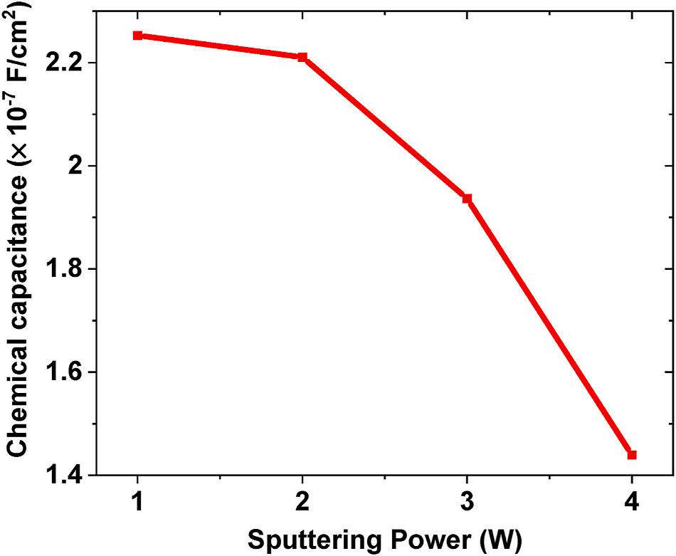
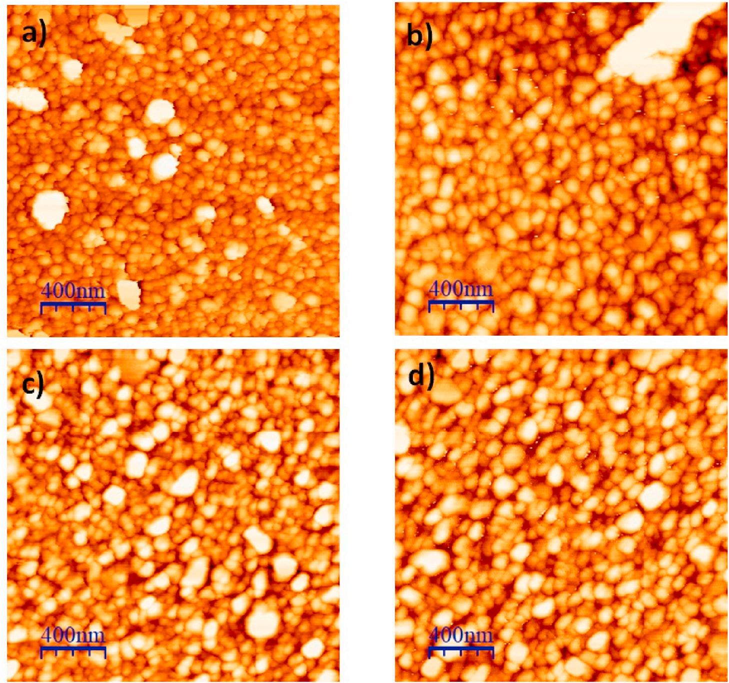
With a further increase in the sputtering power from 3.0 to 4.0 W, the PCE of the cells drastically decreased due to significant reduction in Voc and FF, even though the sheet resistance of the Ag contact has further reduced. SEM examination reveals that the HTL thickness is reduced to about 75 nm after Ag deposition using sputtering power of 4.0 W as shown in Fig. 3 (d) and Table S1 The result indicates that the organic HTL had been severely damaged by Ag particles during high power sputtering. A consequence of the damage to the HTL is an increase in charge recombination, leading to a decrease in charge carrier density of the devices [23]. Fig. 4 shows the chemical capacitance of the devices as a function of the sputtering power. The chemical capacitances were determined from impedance spectroscopy measurements (see Fig. S4 in supplementary information), which is proportional to the charge carrier density. A decrease in the chemical capacitance indicates a reduction in charge carrier density due to an increased charge recombination. The XRD analysis of the Ag films deposited on pure glass substrates at different sputtering powers show clearly that all films are crystalline materials (see Fig. S5). In addition, the thickness of the films and grain size increase with increasing the sputtering power as indicated by the growing peak intensity and the full width at half maximum (FWHM). The data extracted from AFM images show that the grain size of the Ag films increases with increasing sputtering power (Table S2). The AFM
images in Fig. 5 (a)-(d) also show that Ag film deposited at 1.0 W has the most uniform grains, which may also contribute to the observed improvement. These results demonstrate that 1.0 W is the optimum sputtering power for depositing Ag contact on PSCs for the equipment used. It is to be noted that the sheet resistance of the Ag contact prepared using 4.0 W is lower than that using 1.0 W. The results from this work seem to indicate that the difference in the electrical resistance obtained using 1.0 W and 4.0 W has little influence on the performance of the perovskite solar cells because the electrical resistance obtained from 1.0 W is already sufficiently low.

In this part of the experiment, the argon flow rate was varied from 5.0 to 25.0 sccm while the argon pressure, sputtering power and duration were kept at 5.0 mTorr, 1.0 W and 60 min, respectively. The J-V characteristics of PSCs as a function of argon flow rate are shown in Fig. 6 (a) with the device parameters summarized in Table 2 From the results, it can be seen that the PCE and Jsc of the devices are improved as the argon flow rate changes from 5.0 to 25.0 sccm. The improvement may be attributed to a reduction in the sheet resistance of Ag film as shown in Fig. 6 (b).
The Voc remains more or less constant when argon flow rate changes from 5.0 to 15.0 sccm but decreases as the argon flow rate is further raised to 25.0 sccm, while the FF shows an increasing trend with the argon flow rate from 5.0 to 15.0 sccm and begins to reduce as the argon flow rate is at 25.0 sccm. Such variation may be explained by the tradeoff between the sheet resistance of Ag contact and the damage of the HTL. Fig. 6 (b) shows that the sheet resistance of the Ag films decreases with an increase in the argon flow rate, which helps to improve the charge carrier extraction. However, the HTL damage is anticipated to increase with increasing argon flow rate due to an increase in deposition
Fig. 2. Effect of sputtering power on (a) J-V characteristics of the best devices and (b) the thickness of hole transport layer (HTL) and the sheet resistance of Ag films deposited on pure glass substrates.
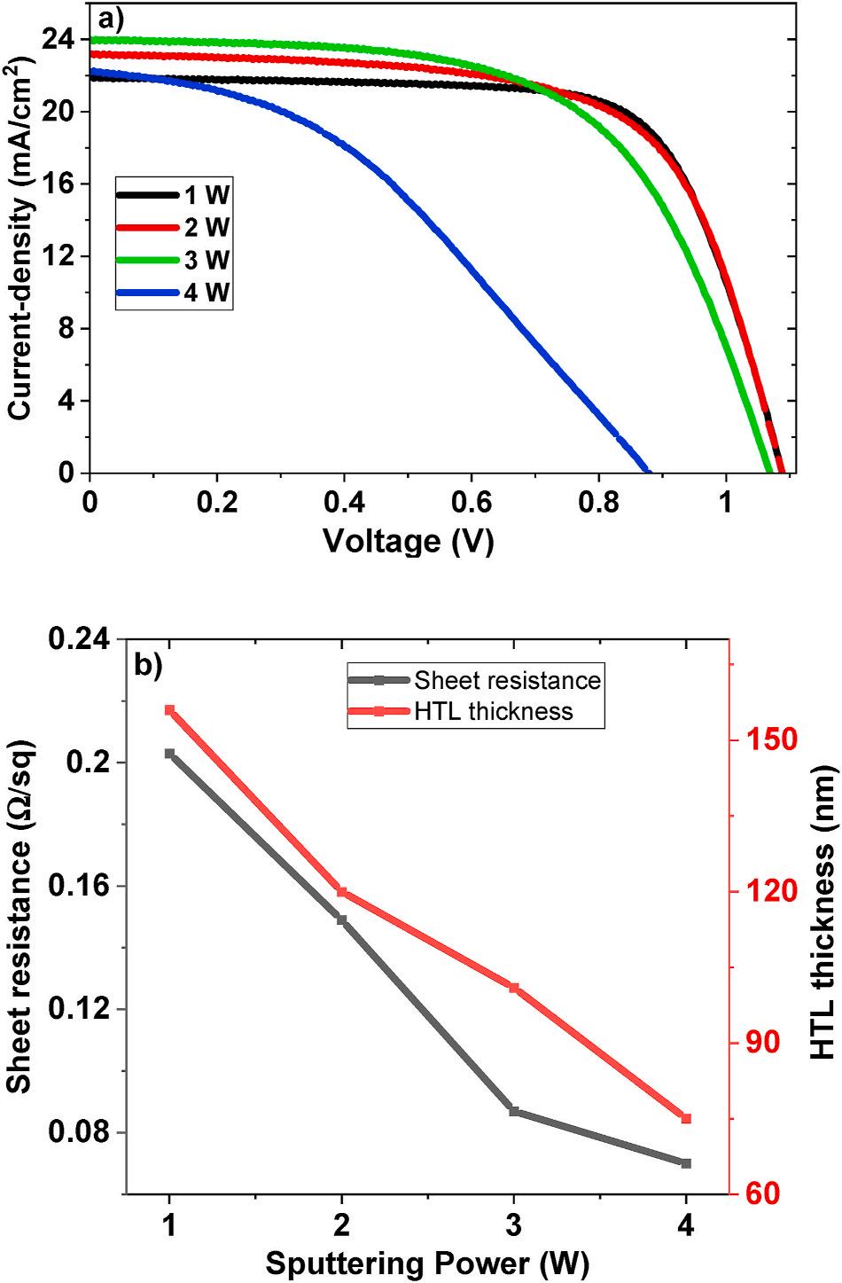
Table 1 Photovoltaic parameters of the devices with Ag contacts deposited on the top of the perovskite/Spiro-OMETAD layers using different sputtering powers (the rows denoted “Best” represent the data obtained from the best solar cells of the batch; the rows denoted “Av” represent the average of all cells in a batch).
Sputtering Power (W)
Voc (V) Jsc (mA/ cm2)
FF (%) Rs (Ω) Rp (kΩ) PCE (%)
1.0 Best 1.09 21.90 70.55 55 40.0 16.82 Av 1.08 ± 0.01 21.44 ± 0.61 69.08 ± 0.85 16.01 ± 0.5
2.0 Best 1.09 23.21 65.24 55 12.5 16.49 Av 1.08 ± 0.01 22.40 ± 1.10 62.28 ± 4.35 15.08 ± 0.83
3.0 Best 1.07 23.96 60.00 67 8.9 15.41 Av 1.07 ± 0.01 23.13 ± 0.74 60.08 ± 1.66 15.05 ± 0.29
4.0 Best 0.88 22.29 38.75 164 1.6 7.61 Av 0.86 ± 0.03 21.22 ± 0.85 37.62 ± 1.00 6.88 ± 0.38
rate, leading to the deterioration of the charge carrier extraction. As a result, the optimal rate is obtained at 15 sccm. Impedance spectroscopy measurements shows that the chemical capacitance of the devices peaks at the argon flow rate of 15 sccm as shown in Fig. 6 (b), indicating that the maximum charge carrier density of devices is obtained at 15 sccm. In summary, 15.0 sccm is the optimum argon flow rate to prepare Ag contact using magnetron sputtering for given conditions under 5.0
Fig. 3. SEM images of the perovskite solar cells with Ag contacts deposited on the top of the perovskite/Spiro-OMETAD layers using magnetron sputtering using the sputtering power at (a) 1.0 W (b) 2.0 W (c) 3.0 W and (d) 4.0 W.
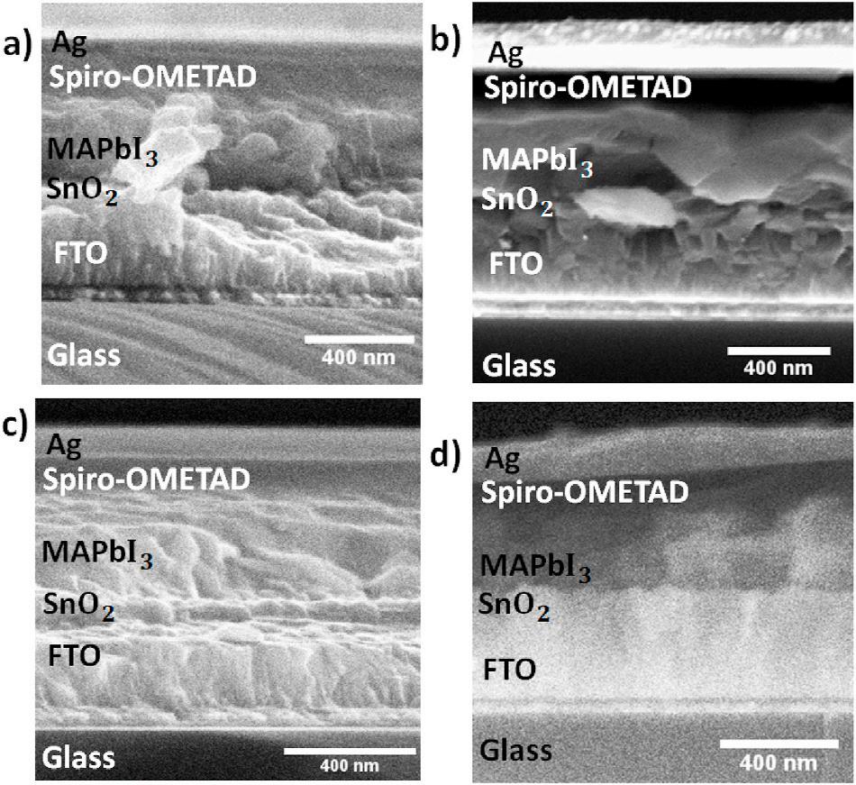
Fig. 4. The chemical capacitance of a perovskite solar cell as a function of sputtering power of magnetron sputtering for Ag contact deposition on the top of perovskite/Spiro-OMETAD layers. The reduction in chemical capacitance indicates a reduction in the charge carrier density.
mTorr, 1.0 W and 60 min.
In this study, sputtering duration was varied from 20 to 80 min while the sputtering pressure, argon flow rate and pressure were kept constant at 1.0 W, 15 sccm and 5 mTorr, respectively. The J-V characteristics of PSCs for different sputtering durations are shown in Fig. 7 (a) and the photovoltaic parameters summarized in Table 3. It can be seen that the Voc, Jsc, and FF of the devices reach their maximum values at a sputtering duration of 40 min, resulting in a remarkable PCE of 18.35% for air-processed PSCs. As shown in Table 3, this efficiency corresponds to a favourable combination of lowest series resistance, Rs, and highest parallel resistance, Rp. It can be seen from Fig. 7 (b) that the chemical capacitance of the devices peaked at 40 min, indicating the optimal period to obtain the maximum charge carrier density. The key reason for
the significant improvement in the PCE arises from a reduction in the power losses associated with the series and parallel resistances. The optimised deposition conditions, in this case, enable to achieve sufficiently low sheet resistance of Ag contact (Fig. 7 (b)) without significant damage to the HTL and the interfacial quality between the HTL and Ag film, which are prone to the damage by particle impact or stress. Any deviation from the optimal deposition conditions would result in an increase in the series resistance and a decrease in parallel resistance as shown in Table 3. Evidently, 40 min is the optimum sputtering duration for Ag deposition for the above-mentioned deposition conditions.
In this part of the experiment, argon pressure was varied from 4.0 to 7.0 mTorr while the sputtering power, duration and argon flow rate were kept at 1.0 W, 40 min and 15.0 sccm, respectively. The J-V characteristics of PSCs for different argon pressures are shown in Fig. 8 (a) with the device parameters summarized in Table 4. It can be seen that the Voc, FF and PCE of the devices are increased as the argon pressure changes from 4.0 to 5.0 mTorr while the Jsc remains unchanged. This may be attributed to possible HTL damage due to deposition at low argon pressure (4.0 mTorr in this case) resulting in poor charge carrier extraction as shown in Fig. 8 (b) [25]. At low argon pressure, Ag particles suffer less scattering by Ar ions and reach HTL surface with high impact. When the argon pressure is 5.0 mTorr, the kinetic energy of Ag particles is reduced due to increased scattering by Ar ions, resulting in less damage to the HTL and consequently improvement in Voc, FF and PCE and good charge carrier extraction as shown in Fig. 8 (b). As the argon pressure is further increased to 7.0 mTorr, less damage to the HTL is expected. However, the sheet resistance of Ag films increased
significantly, resulting in poor charge carrier extraction as indicated by lower chemical capacitance shown in Fig. 8 (b). This is possibly due to poor morphology arising from disconnected grains and longer deposition duration, the morphology is likely to improve as has been reported [20]. Based on the results obtained in this study, it can be concluded that the argon pressure has a significant influence on the performance of the PSC devices and 5 mTorr is the optimum pressure for Ag contact deposition.
We studied the effect of Ag electrode deposition parameters on the performances of perovskite solar cells using magnetron sputtering. It is found that the best performance is achieved using sputtering power of 1.0 W, argon flow rate of 15sccm, sputtering duration of 40 min and argon pressure of 5mTorr, resulting in a power conversion efficiency of 18.4%. The devices also exhibit an excellent short-circuit current density of 22.56 mA/cm2, the open-circuit voltage of 1.1 V and a fill factor of 73.7%. It is worth noting that all fabrication processes in this work were carried out in the air, except for Ag contact deposition. The efficiency of 18.4% represents one of the highest efficiencies reported under such conditions. This result demonstrates that through the systematic optimisation of the above parameters, high performance perovskite solar cells can be fabricated using magnetron sputtering for preparation of the metal electrode. This work provides a guide on the fabrication of high performance and air processed PSCs relevant to practical applications. The key challenge is to determine the appropriate deposition parameters, which involves a careful trade-off between achieving low sheet resistance and minimising the damage to the HTL. Damage to HTL layer leads to the formation of interfacial defects which correlate with the s-
Fig. 6. Effect of argon flow rate of magnetron sputtering deposition on (a) J-V characteristics of best devices and (b) the chemical capacitance of devices and the sheet resistance of Ag films deposited on pure glass substrates. The change in chemical capacitance represent the similar change in the charge carrier density.
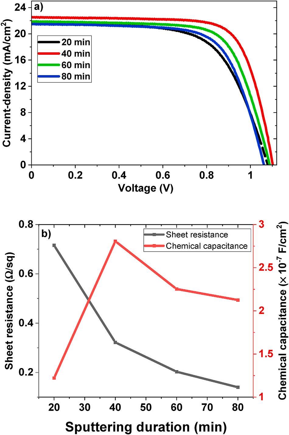
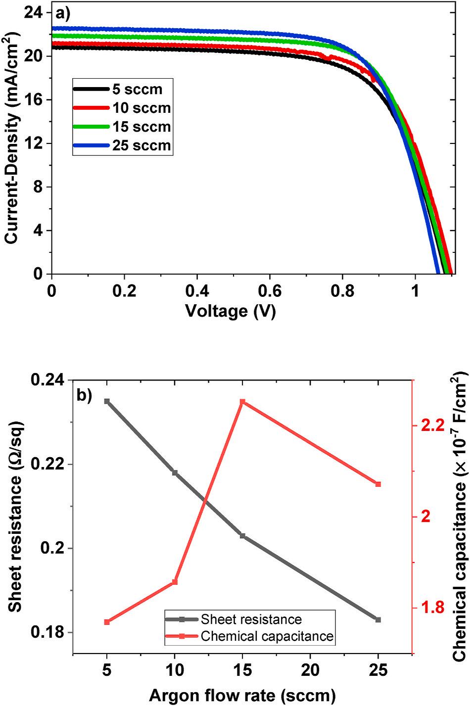
Table 2
Photovoltaic parameters of devices with Ag contacts deposited on the top of the perovskite/Spiro-OMETAD layers using different argon flow rates (the rows denoted “Best” represent the data obtained from the best solar cells of the batch; the rows denoted “Av” represent the average of all cells in a batch).
Argon flow rate (sccm) Voc (V) Jsc (mA/ cm2)
FF (%) Rs (Ω) Rp (kΩ) PCE (%)
5.0 Best 1.09 20.84 68.22 55 7.4 15.44 Av 1.09 ± 0.01 20.42 ± 1.18 64.71 ± 2.66 14.39 ± 1.21
10.0 Best 1.10 21.22 69.03 56 22.6 16.12 Av 1.08 ± 0.02 20.63 ± 0.73 65.82 ± 2.71 14.70 ± 0.97
15.0 Best 1.09 21.90 70.55 55 40.0 16.82 Av 1.08 ± 0.01 21.44 ± 0.61 69.08 ± 0.85 16.01 ± 0.52
25.0 Best 1.06 22.56 70.32 49 21.9 16.91 Av 1.06 ± 0.01 23.01 ± 0.99 63.27 ± 5.12 15.45 ± 0.97
shape JV curve at 4W.
Martin C. Eze: Major experimental work and data analysis, Conceptualization, Methodology, Data curation, Writing – original
Fig. 7. Effect of sputtering duration of magnetron sputtering deposition on (a) J-V characteristics of the best devices and (b) the chemical capacitance of the devices and the sheet resistance of Ag films deposited on pure glass substrates. The change in chemical capacitance represent the similar change in the charge carrier density.
Table 3
Photovoltaic parameters of devices with Ag contacts deposited on the top of the perovskite/Spiro-OMETAD layers using different sputtering duration (the rows denoted “Best” represent the data obtained from the best solar cell of the batch; the rows denoted “Av” represent the average of all cells in a batch).
Sputtering duration (min)
Voc (V) Jsc (mA/ cm2)
FF (%) Rs (Ω) Rp (kΩ) PCE (%)
20 Best 1.08 21.73 64.04 68 7.1 15.02 Av 1.08 ± 0.01
19.65 ± 1.06 65.27 ± 2.20 13.84 ± 0.56
40 Best 1.10 22.56 73.70 45 60.0 18.35 Av 1.09 ± 0.02
22.18 ± 0.93 70.25 ± 2.29 16.99 ± 0.98
60 Best 1.09 21.90 70.55 55 40.0 16.82 Av 1.08 ± 0.01
21.44 ± 0.61 69.08 ± 0.85 16.01 ± 0.52
21.28 ± 1.03 65.93 ± 1.76 14.53 ± 0.49
draft, Scholarship acquisition, Writing – review & editing. Godwin Ugwuanyi: Data curation, Writing – review & editing. Meng Li: Conceptualization, Writing – review & editing. Hyginus U. Eze: Data
Fig. 8. Effect of argon pressure of magnetron sputtering deposition on (a) J-V characteristics of the best devices and (b) the chemical capacitance of the devices and the sheet resistance of Ag films deposited on pure glass substrates. The change in chemical capacitance represent the similar change in the charge carrier density.
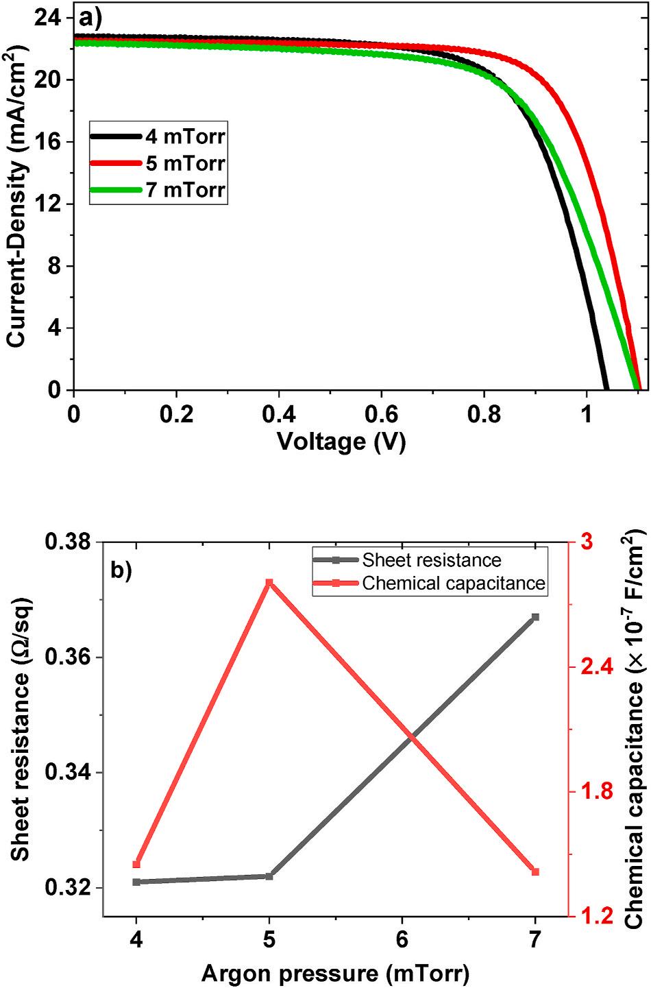
Table 4
Photovoltaic parameters of devices with Ag contacts deposited on the top of the perovskite/Spiro-OMETAD layers using different argon pressures (the rows denoted “Best” represent the data obtained from the best solar cells of the batch; the rows denoted “Av” represent the average of all cells in a batch).
Ar pressure (mTorr) Voc (V) Jsc (mA/ cm2)
FF (%) Rs (Ω) Rp (kΩ) PCE (%)
4.0 Best 1.04 22.86 69.70 46 14.4 16.57 Av 1.04 ± 0.01 21.56 ± 0.97 68.93 ± 1.19 15.52 ± 0.86
5.0 Best 1.10 22.56 73.70 45 60.0 18.35 Av 1.09 ± 0.02 22.18 ± 0.93 70.25 ± 2.29 16.99 ± 0.98
7.0 Best 1.10 22.42 66.57 64 29.3 16.43 Av 1.08 ± 0.01 20.24 ± 1.68 64.59 ± 1.76 14.19 ± 1.35
curation, Writing – review & editing. Guillermo M. Rodriguez: Methodology, Writing – review & editing. Alex Evans: Methodology. Victoria G. Rocha: Supervision, Resources, Writing – review & editing. Zhe Li: Supervision, Funding acquisition, Recourses, Conceptualization, Writing – review & editing. Gao Min: Supervision, Funding acquisition, Resources, Project administration, Conceptualization, Validation, Major review & editing.
The authors declare that they have no known competing financial interests or personal relationships that could have appeared to influence the work reported in this paper.
One of the authors (MCE) would like to thank the Federal Government of Nigeria for the financial support of his PhD study under the Petroleum Technology Development Fund PTDF/ED/PHD/EMC/1091/ 17. Dr D Sapsford and Mr J Rowland are thanked for assistance in XRD and UV–Vis spectroscopy. Dr E Brousseau is thanked for assistance in SEM. Dr Barbe Jeremy is thanked for the training offered to MCE. EPSRC and Welsh Government are acknowledged for partial support of facilities for fabrication and characterisation of solar cells under the projects EP/ K029142/1, EPK022156/1, and Ser Cymru II (Z Li).
Supplementary data to this article can be found online at https://doi. org/10.1016/j.solmat.2021.111185
[1] S. Wang, L. Pan, J.J. Song, W. Mi, J.J. Zou, L. Wang, et al., Titanium-defected undoped anatase TiO2with p-type conductivity, room-temperature ferromagnetism, and remarkable photocatalytic performance, J. Am. Chem. Soc. 137 (2015) 2975–2983, https://doi.org/10.1021/ja512047k
[2] N. Zhang, W. Sun, S.P. Rodrigues, K. Wang, Z. Gu, S. Wang, et al., Highly reproducible organometallic halide perovskite microdevices based on top-down lithography, Adv. Mater. 29 (2017) 9–10, https://doi.org/10.1002/ adma.201606205
[3] G.E. Eperon, S.D. Stranks, C. Menelaou, M.B. Johnston, L.M. Herz, H.J. Snaith, Formamidinium lead trihalide: a broadly tunable perovskite for efficient planar heterojunction solar cells, Energy Environ. Sci. 7 (2014) 982, https://doi.org/ 10.1039/c3ee43822h
[4] D. Li, F. Sun, C. Liang, Z. He, Effective approach for reducing the migration of ions and improving the stability of organic-inorganic perovskite solar cells, J. Alloys Compd. 741 (2018) 489–494, https://doi.org/10.1016/j.jallcom.2018.01.082
[5] M. Alidaei, M. Izadifard, M.E. Ghazi, V. Ahmadi, Efficiency enhancement of perovskite solar cells using structural and morphological improvement of CH3NH3PbI3 absorber layers, Mater. Res. Express 5 (2018), https://doi.org/ 10.1088/2053-1591/aaa616
[6] A. Kojima, K. Teshima, Y. Shirai, T. Miyasaka, Organometal halide perovskites as visible-light sensitizers for photovoltaic cells, J. Am. Chem. Soc. 131 (2009) 6050–6051, https://doi.org/10.1021/ja809598r
[7] N.J. Jeon, H. Na, E.H. Jung, T.Y. Yang, Y.G. Lee, G. Kim, et al., A fluoreneterminated hole-transporting material for highly efficient and stable perovskite solar cells, Nature Energy 3 (2018) 682–689, https://doi.org/10.1038/s41560018-0200-6
[8] Q. Jiang, Y. Zhao, X. Zhang, X. Yang, Y. Chen, Z. Chu, et al., Surface passivation of perovskite film for efficient solar cells, Nat. Photonics 13 (2019), https://doi.org/ 10.1038/s41566-019-0398-2
[9] M. Jeong, I.W. Choi, E.M. Go, Y. Cho, M. Kim, B. Lee, et al., Stable perovskite solar cells with efficiency exceeding 24.8% and 0.3-V voltage loss, Science 369 (2020) 1615–1620
[10] NREL. Best Research-Cell Efficiencies, National Renewable Energy Laboratory, vol. 1, 2020. https://www.nrel.gov/pv/cell-efficiency.html
[11] M. Saliba, T. Matsui, J.-Y.Y. Seo, K. Domanski, J.-P.P. Correa-Baena, M. K. Nazeeruddin, et al., Cesium-containing triple cation perovskite solar cells: improved stability, reproducibility and high efficiency, Energy Environ. Sci. 9 (2016) 1989–1997, https://doi.org/10.1039/C5EE03874J
[12] W.S. Yang, B. Park, E.H. Jung, N.J. Jeon, Iodide management in formamidiniumlead-halide – based perovskite layers for efficient solar cells, Science 356 (2017) 1376–1379, https://doi.org/10.1126/science.aan2301
[13] A.D. Jodlowski, C. Rold´ an-Carmona, G. Grancini, M. Salado, M. Ralaiarisoa, S. Ahmad, et al., Large guanidinium cation mixed with methylammonium in lead iodide perovskites for 19% efficient solar cells, Nature Energy 2 (2017) 972–979, https://doi.org/10.1038/s41560-017-0054-3
[14] P. Chen, Y. Bai, S. Wang, M. Lyu, J.-H. Yun, L. Wang, In situ growth of 2D perovskite capping layer for stable and efficient perovskite solar cells, Adv. Funct. Mater. 1706923 (2018) 1706923, https://doi.org/10.1002/adfm.201706923.
[15] Y. Cai, S. Wang, M. Sun, X. Li, Y. Xiao, Mixed cations and mixed halide perovskite solar cell with lead thiocyanate additive for high efficiency and long-term moisture stability, Org. Electron. 53 (2018) 249–255, https://doi.org/10.1016/j. orgel.2017.11.045
[16] Z. Zhang, Y. Zhou, Y. Cai, H. Liu, Q. Qin, X. Lu, et al., Efficient and stable CH3NH3PbI3-x(SCN)x planar perovskite solar cells fabricated in ambient air with low-temperature process, J. Power Sources 377 (2018) 52–58, https://doi.org/ 10.1016/j.jpowsour.2017.11.070
[17] F. Wang, Z. Ye, H. Sarvari, S.M. Park, A. Abtahi, K. Graham, et al., Humidityinsensitive fabrication of efficient perovskite solar cells in ambient air, J. Power Sources 412 (2019) 359–365, https://doi.org/10.1016/j.jpowsour.2018.11.013
[18] D.H. Kim, J.H. Heo, S.H. Im, Hysteresis-less CsPbI2Br mesoscopic perovskite solar cells with a high open-circuit voltage exceeding 1.3 v and 14.86% of power conversion efficiency, ACS Appl. Mater. Interfaces 11 (2019) 19123–19131, https://doi.org/10.1021/acsami.9b03413
[19] T. Wahl, J. Hanisch, E. Ahlswede, Comparison of the Al back contact deposited by sputtering, e-beam, or thermal evaporation for inverted perovskite solar cells, J. Phys. Appl. Phys. 51 (2018), https://doi.org/10.1088/1361-6463/aab0d8.
[20] Y. Mo, J. Shi, P. Zhou, S. Li, T. Bu, Y.-B. Cheng, et al., Efficient planar perovskite solar cells via a sputtered cathode, Solar RRL 3 (2019) 1900209, https://doi.org/ 10.1002/solr.201900209
[21] E. Baudet, M. Sergent, P. Nemec, C. Cardinaud, E. Rinnert, K. Michel, et al., Experimental design approach for deposition optimization of RF sputtered chalcogenide thin films devoted to environmental optical sensors, Sci. Rep. 7 (2017) 1–14, https://doi.org/10.1038/s41598-017-03678-w
[22] D. Benetti, R. Nouar, R. Nechache, H. Pepin, A. Sarkissian, F. Rosei, et al., Combined magnetron sputtering and pulsed laser deposition of TiO2 and BFCO thin films, Sci. Rep. 7 (2017) 2–10, https://doi.org/10.1038/s41598-017-02284-0
[23] S. Yang, Y. Yu, Z. Ni, L. Lei, M. Li, Q. Wei, et al., Influence of hole transport material/metal contact interface on perovskite solar cells, Nanotechnology 29 (2018) 255201, https://doi.org/10.1088/1361-6528/aab795
[24] L. Wang, G.R. Li, Q. Zhao, X.P. Gao, Non-precious transition metals as counter electrode of perovskite solar cells, Energy Storage Materials 7 (2017) 40–47, https://doi.org/10.1016/j.ensm.2016.11.007
[25] F. Behrouznejad, S. Shahbazi, N. Taghavinia, H. Wu, E.W. Diau, A study on utilizing different metals as the back contact of CH3NH3PbI3 perovskite solar cells, J. Mater. Chem. 4 (2016) 13488–13498, https://doi.org/10.1039/c6ta05938d
[26] I. Jeong, H. Jin Kim, B.S. Lee, H. Jung Son, J. Young Kim, D.K. Lee, et al., Highly efficient perovskite solar cells based on mechanically durable molybdenum cathode, Nanomater. Energy 17 (2015) 131–139, https://doi.org/10.1016/j. nanoen.2015.07.025
[27] Q. Jiang, X. Sheng, B. Shi, X. Feng, T. Xu, Nickel-cathoded perovskite solar cells, J. Phys. Chem. C 118 (2014) 25878–25883, https://doi.org/10.1021/jp506991x.
[28] P. Qin, Q. He, G. Yang, X. Yu, L. Xiong, G. Fang, Metal ions diffusion at heterojunction chromium oxide/CH3NH3PbI3 interface on the stability of perovskite solar cells, Surfaces and Interfaces 10 (2017) 93–99, https://doi.org/ 10.1016/j.surfin.2017.12.006
[29] S. Bao, J. Wu, X. He, Y. Tu, S. Wang, M. Huang, et al., Mesoporous Zn2SnO4 as effective electron transport materials for high-performance perovskite solar cells,
Electrochim. Acta 251 (2017) 307–315, https://doi.org/10.1016/j. electacta.2017.08.083
[30] M.H. Li, J.H. Yum, S.J. Moon, P. Chen, Inorganic p-type semiconductors: their applications and progress in dye-sensitized solar cells and perovskite solar cells, Energies 9 (2016) 1–28, https://doi.org/10.3390/en9050331
[31] H. Lee, S. Rhee, J. Kim, C. Lee, H. Kim, Surface coverage enhancement of a mixed halide perovskite film by using an UV-ozone treatment, J. Kor. Phys. Soc. 69 (2016) 406–411, https://doi.org/10.3938/jkps.69.406
[32] X. Li, S.M. Dai, P. Zhu, L.L. Deng, S.Y. Xie, Q. Cui, et al., Efficient perovskite solar cells depending on TiO2 nanorod arrays, ACS Appl. Mater. Interfaces 8 (2016) 21358–21365, https://doi.org/10.1021/acsami.6b05971
[33] Q. Jiang, T. Xu, Organic-Inorganic hybrid perovskite materials for “nova star” solar cells: state of Technology and outstanding challenges, Comments Mod. Chem. 36 (2016) 200–214, https://doi.org/10.1080/02603594.2015.1116985.
[34] L.-C. Chen, Z.-L. Tseng, J.-K. Huang, A study of inverted-type perovskite solar cells with various composition ratios of (FAPbI3)1 x(MAPbBr3)x, Nanomaterials 6 (2016) 183, https://doi.org/10.3390/nano6100183
[35] K. Poorkazem, T.L. Kelly, Improving the stability and decreasing the trap state density of mixed-cation perovskite solar cells through compositional engineering, Sustainable Energy & Fuels 1 (2018), https://doi.org/10.1039/C8SE00127H
[36] S. Haya, O. Brahmia, O. Halimi, M. Sebais, B. Boudine, Sol-gel synthesis of Srdoped SnO 2 thin films and their photocatalytic properties, Mater. Res. Express 4 (2017), https://doi.org/10.1088/2053-1591/aa8deb
[37] J. Jimenez-Lopez, W. Cambarau, L. Cabau, E. Palomares, Charge injection, carriers recombination and HOMO energy level relationship in perovskite solar cells, Sci. Rep. 7 (2017) 1, https://doi.org/10.1038/s41598-017-06245-5
[38] X. Hou, S. Huang, W. Ou-Yang, L. Pan, Z. Sun, X. Chen, Constructing efficient and stable perovskite solar cells via interconnecting perovskite grains, ACS Appl. Mater. Interfaces 9 (2017) 35200–35208, https://doi.org/10.1021/ acsami.7b08488
[39] Q. Sun, S. Zhou, X. Shi, X. Wang, L. Gao, Z. Li, et al., Efficiency enhancement of perovskite solar cells via electrospun CuO nanowires as buffer layers, ACS Appl. Mater. Interfaces (2018), https://doi.org/10.1021/acsami.7b19335 acsami.7b19335.
[40] Y. Chen, W. Wu, R. Ma, C. Wang, Perovskites fabricated with volatile anti-solvents for more efficient solar cells, J. Mol. Struct. 1175 (2018) 632–637, https://doi.org/ 10.1016/J.MOLSTRUC.2018.08.021
[41] J.F. Wang, L. Zhu, B.G. Zhao, Y.L. Zhao, J. Song, X.Q. Gu, et al., Surface engineering of perovskite films for efficient solar cells, Sci. Rep. 7 (2017) 1–9, https://doi.org/10.1038/s41598-017-14920-w
[42] J. Nelson, The Physics of Solar Cells, first ed., Imperial College Press, London, 2003
[43] J. Wang, J. Li, X. Xu, Z. Bi, G. Xu, H. Shen, Promising photovoltaic application of multi-walled carbon nanotubes in perovskites solar cells for retarding recombination, RSC Adv. 6 (2016) 42413–42420, https://doi.org/10.1039/ c6ra04743b