
BODY ANTENNA WITH DGS FOR BODY CENTRIC WIRELESS COMMUNICATION SYSTEM
Hitesh Joshi [1], Ravindra Prakash Gupta [2]Research Scholar, Pacific University, Udaipur (Raj.),India[1], Manda Institute of Technology, Bikaner(Raj), India[2]
ABSTRACT
This paper presents modified patch antenna for 3 GHz and 5 GHz operating frequencies. Here different approaches are studied by varying slot sizes, defected ground size, notch and also changing feed position. Insertion of slots gives dual frequency operation. Notch provides shifting of lower frequency band towards left hand side. Here combined effect of each techniques adopted gives desired result. Proposed antenna resonates for 3 and 5 GHz frequency. Simulation is done using IE3D software for various parameters. Return loss of final design was -12.17 dB for 3 GHz frequency and VSWR of 1.65. For 5 GHz simulation response was -10.04dB return loss and VSWR of 1.91. Proposed antenna is fabricated giving different details. Paper gives good agreement between measured and simulated results.
KEYWORDS
Body Antenna, Patch, slot, DGS, feed line, center, Body centric wireless communication
1. INTRODUCTION
Patch antenna is a important part of mixer as it is used as receiver of RF signal from space. In high-performance aircraft, spacecraft, satellite, and missile applications, where size, weight, cost, performance, ease of installation, and aerodynamic profile are constraints, low-profile antennas may be required. Presently there are many other government and commercial applications, such as mobile radio and wireless communications that have similar specifications. It works as body antenna as installation is quite easier.
Good body antenna requires thick substrate means lower dielectric constant this is because it fits according to the need of design. They are soft so easily drilling is possible. It provides better efficiency, larger bandwidth, loosely bound fields for radiation into space, but at the expense of larger element size. There are many configurations that can be used to feed microstrip antennas. There are four most popular feeding microstrip line, coaxial probe, aperture coupling, and proximity feed. In the proposed antenna microstrip feed line was used. The microstrip feed line is also a conducting strip, usually of much smaller width compared to the patch. The microstrip-line feed is easy to fabricate, simple to match by controlling the inset position and rather simple to model.
The standard FR-4 substrate material has been mostly used as low cost material for analog and digital circuit design for lower frequencies because of relative high dissipation loss and dielectric constant variation. Resin is combined with high-quality core materials like fine glass fabrics or aramid. Meanwhile, resin-based substrates with enhanced electrical properties are commercially available for high frequency applications ensuring low dissipation loss over a broad frequency range. The substrate height determines the width of the microstrip line for given characteristic impedance. The design of low impedance microstrip lines can result in very wide strips with cutoff frequencies of higher-order modes within or near the operating frequency range. With narrow microstrip lines on thick substrates, the risk of undesired parasitic effects occurs. When the substrate thickness h reaches a quarter-wavelength, then the dielectric-cladded metal plate forms an open-ended resonator in normal direction with respect to the substrate surface, which would be prone to radiating electromagnetic energy. For a high dielectric constant, the dielectricair interface acts like a magnetic wall for the resonating field.
2. DESIGN
Different dimensions can be calculated by standard formulas. For an efficient radiator, a practical width that leads to good radiation efficiencies is
where υ0 is the free-space velocity of light.
W
Determine the effective dielectric constant of the microstrip antenna using relation,
Once W is found, determine the extension of the length 3L by formula
" #$$ %.&'() * %. +,-
= 0.044 mm
The actual length (L)of the patch can be determined by
L= 26.525 mm
Leff = 27.376 mm
3. SOFTWARE AND STEPS
For Simulation IE3D software was used as it helps in 3D designing. IE3D is a full-wave electromagnetic simulator based on the method of moments, solution of integral equation which has an excellent accuracy for frequency domain analysis. It analyzes 3D and multilayer structures of general shapes. Thus, if the structure is simple like rectangular or circular means any regular shape, IE3D would be the best. Defining the ports is easy in IE3D software. IE3D has full-3D modeling for finite substrates and can handle many 3D problems. It has been widely used in the design of MICs, RFICs, patch antennas, wire antennas, and other RF/wireless antennas. Various parameters such as S11, VSWR, current distributions as well as the radiation patterns can be find out.
Figure 1 shows the steps of the computer aided circuit design of microwave circuits. The circuit analysis delivers the response function in terms of the component parameters, circuit topology, and independent excitations. The circuit analysis delivers the response of the circuit, and the result is compared with the design goals. If the agreement is not satisfying, then some relevant circuit parameters have to be changed in an iterative way.
This design phase is termed as optimization. Optimization describes an iterative change of network parameters, to obtain a specified circuit performance. It focuses on error minimization of actually reached circuit data and the specified objective function.
The iterative procedure of circuit analysis, specification comparison, and optimization is continued as long as the specifications have been met. Then the circuit is fabricated and measured. If the measurement result is not satisfying, then further modifications must be introduced. Such investigations are important to analyze the influence of processing tolerances on the circuit properties [6].
A. First Approach
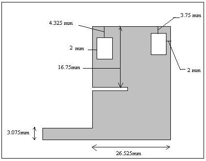
Two square slots of size 5mm each side were cut. Along with that on the top right corner was cut with dimension 2.52 mm and 4.52 mm. Here the position of microstrip line was at the standard position. Size of defected ground was 13mm width and 30 mm length.

Here blue layer is for the conducting layer and green layer for the
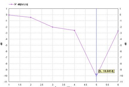
Observed VSWR was 1.91 at 5 GHz instead of 3GHz frequency. So some other modification was required.
B. Second Approach
Now here modification is done in two different plane i.e. on top plane and ground plane separately. For top plane two square slots of size 5mm x 5mm are made on upper portion Of the rectangular patch antenna. Also a rectangular slot is made at a distance of 16.75 mm from top margin. Dimension of this slot is 1 mm x 12.75mm.
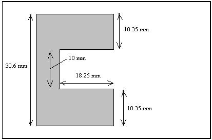
Ground plane is made defected. Here ground plane is shifted beneath the microstrip line feed with dimension of 30.6 mm width and 26.525 mm length. A rectangular defected structure of dimension 10 mm width and 18 mm length is made in the ground plane.
VSWR was found to be 1.65.
Also the position of feed line was changed from centre to lower edge. This will help in impedance matching helping to improve the performance of patch antenna. By changing the position of the line feed location there occur variations in the impedance on smith chart. It also varies the return loss of the antenna which affects the bandwidth of the antenna. Polarization is linear as feed was not placed diagonal corner but lower corner of patch.
The notch or shape which cuts in the patch affects the antenna parameter. Here we cut the square at both the radiating edge of the feed patch. The graph below shows the variation in return loss as well as variation in the impedance of the antenna.
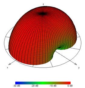
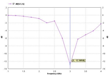
The value of S11 was good from the frequency 2.895 GHz to 3.105 GHz for which the value is equal to -10 dB. So bandwidth in this case was 210 MHz. VSWR is a measure of how many power is delivered to an antenna. This does not show that the antenna radiates all power it receives. VSWR measures the potential to radiate. A low VSWR means the antenna is wellmatched.
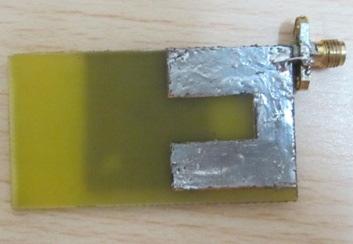
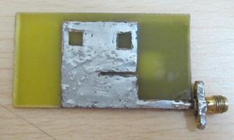
4. MEASURED RESULTS
Figure shows photographs of fabricated proposed antenna.
CONCLUSION
Modified design of patch antenna with defected ground structure (DGS) and slots on conducting plane provides simulation results having return loss of -12.90 dB and VSWR of 1.62 for 3 GHz. For 5 GHz value of return loss was -10.04 dB and VSWR of 1.91. This antenna can be operated for various application ranges because of dual mode. Measured return loss was -12.71 dB. Also very good results were found at 2.39 GHz frequency.

ACKNOWLEDGEMENT
Authors like to give their thanks to ‘Geetanjali Institute of Technical Studies’, Udaipur (Raj.), India for the support.
REFERENCES
[1] Pozar, D. M., Microwave Engineering, 3rd edition, John Wiley & Sons, Inc 2004.
[2] Balanis, C.A., Antenna Theory, 3rd edition, John Wiley & Sons, Inc 2004.
[3] Chen, X. Q., X. W. Shi, Y. C. Guo, and C. M. Xiao, “A novel dual band transmitter using microstrip defected ground structure,”Progress In Electromagnetics Research, PIER 83, 1–11, 2008.
[4] Oskouei, D., H. K. Forooraghi, and M. Hakak, “Guided and leaky wave characteristics of periodic defected ground structures,” Progress In Electromagnetics Research, PIER 73, 15–27, 2007.
[5] Fooks, E. H. and R. A. Zakarevicius, Microwave Engineering Using Microstrip Circuits, Prentice Hall, 1990.
[6] M. Wegmuller, J. P. von der Weid, P. Oberson, and N. Gisin, “High resolution fiber distributed measurements with coherent OFDR,” in Proc. ECOC’00, 2000, paper 11.3.4, p. 109.
[7] H. Oraizi and M. S. Esfahlan,” Miniaturization of Wilkinson power Dividers by using defected ground structure”, Progress In Electromagnetics Research Letters, Vol. 4, 113–120, 2008SR.
[8] ”Stripline – like Transmission Lines for Microwave Integrated Circuits”, Bharathi Bhat , Shiban K. Koul
[9] J. Clerk Maxwell, A Treatise on Electricity and Magnetism, 3rd ed., vol. 2. Oxford: Clarendon, 1892, pp.68–73.
Author’s Bibliography
Hitesh Joshi S/o Mr. D.S. Joshi is born on 12-10-1982. He completed his B. E in Electronics and Communication Engineering from Rajasthan University, Jaipur, India in year 2004, M.B.A. in HR from I.G.N.O.U. India in year 2009,M. Tech. in VLSI Design from Mewar University, Chittorgarh, India in year 2012 and Pursuing Ph. D. (Electronic and Communication) from Pacific University, Udaipur, India. Presently he is working as Principal in Shri USB College of Engineering & Management, Abu Road and Previously Principal in ,Shree Sadguru Seva Mandal Polytechnic College, Abu Road and Associate Professor and Asst. Prof at Gitanjali Institute of Technical Studies Udaipur, Maharishi Arvind Institute of Engg. & Tech. Jaipur. His area of interests includes Antenna Design, Body Antenna, Wireless Communication, Body Area Network, Body centric wireless communication. He has more than 12 years Academic/Research experience. He has guided several DST projects and dissertations in B. Tech and M. Tech courses. He had published numerous International and National papers.

Ravindra Prakash Gupta S/o Mr. S.P. Gupta was born on 27-10-1973. He completed his B. E in Electronics Engineering from Marathwada University, Aurangabad in year 1998, M. Tech. in Electronic and Communication from Malviya National Institute of Technology, Jaipur, India in year 2004 and Ph. D. (Electronic and Communication) from Bhagwant University, Ajmer, India in year 2012 Presently he is working as Principal and Professor at Manda Institute of Technology, Bikaner and previously at Maharishi Arvind College of Engineering and Research, Sirsi Road, Jaipur. His area of interests includes Signal Processing, Digital Communication, Wireless Communication, Wireless Sensor Networks, Design of Computer Network. He has more than 16 years Academic/Research experience. He has worked with the prestigious Military College of Telecommunication Engineering, Mhow, Indore, India. He is a Life-Member of Indian Society of Technical Education (ISTE), New Delhi and The Institution of Electronics and Telecommunication Engineers (IETE), New Delhi.. He has guided several projects and dissertations in B. Tech and M. Tech courses. He had published numerous International papers in India and abroad and guiding Ph. D. research scholars at reputed Universities. He has actively organized numerous National Conferences in the field of Engineering, Applied Sciences, Energy and Environment
