International Journal of Antennas (JANT) Vol.2, No.1, January 2016
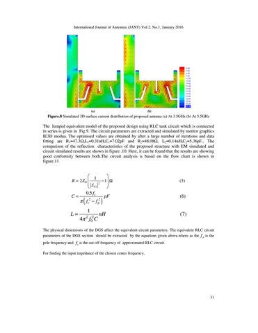
Figure.8 Simulated 3D surface current distribution of proposed antenna (a) At 3.5GHz (b) At 5.5GHz
The lumped equivalent model of the proposed design using RLC tank circuit which is connected in series is given in Fig.9. The circuit parameters are extracted and simulated by mentor graphics IE3D modua. The optimised values are obtained by after a large number of iterations and data fitting are R1=47.3Ω,L1=0.31nH,C1=7.02pF and R2=48.08Ω, L2=0.14nH,C2=5.36pF.. The comparison of the reflection characteristics of the proposed structure with EM simulated and circuit simulated results are shown in figure .10. Here, it can be found that the results are showing good conformity between both.The circuit analysis is based on the flow chart is shown in figure.11 1 R = 2Z0 S 11
C=
L=
2
− 1 Ω
(5)
pF
(6)
0.5 fc
(
π fc2 − f p2
1 2
4π f02C
)
nH
(7)
The physical dimensions of the DGS affect the equivalent circuit parameters. The equivalent RLC circuit parameters of the DGS section should be extracted by the equations given above,where as the f p is the pole frequency and f c is the cut off frequency of approximated RLC circuit. For finding the input impedance of the chosen center frequency,
31