
International Research Journal of Engineering and Technology (IRJET) e-ISSN: 2395-0056
Volume: 13 Issue: 03 | Mar 2026 www.irjet.net p-ISSN: 2395-0072
International Research Journal of Engineering and Technology (IRJET) e-ISSN: 2395-0056
Volume: 13 Issue: 03 | Mar 2026 www.irjet.net p-ISSN: 2395-0072
G. N Sandhya Devi1, T. Sri Rithvik2, S. Prem Chand3, V. Venkata Yaswanth4, Y. Praveen Pal5
1 Assistant Professor, Dept. of Electronics and Communication Engineering, Seshadri Rao Gudlavalleru Engineering College, Gudlavalleru, Andhra Pradesh, India
2,3,4,5 Students, Dept. of Electronics and Communication Engineering, Seshadri Rao Gudlavalleru Engineering College, Gudlavalleru, Andhra Pradesh, India
Abstract - Time-to-Digital Converters (TDCs) are widely used digital circuits for measuring very small-time intervals between signal events in high-precision systems. This project presents the design and implementation of a two-level TDC architecture that combines both coarse and fine time measurement techniques to achieve improved resolution and dynamic range. The coarse measurement is implemented using a counter-based TDC that counts clock cycles between start and stop signals, offering simplicity and a wide measurement range but limited resolution. To overcome this limitation, a fine measurement stage is introduced using a buffer delay line, which subdivides a single clock period into smaller intervals based on the known propagation delay of logic gates. The hybrid TDC combines these approaches to achieve improved resolution and an extended measurement range, making it suitable for applications such as time-of-flight measurements, digital communication systems, radar systems and precision instrumentation. However, the hybrid architecture results in higher power consumption due to increased switching activity. To address this issue, a flip-flop based clock gating technique is proposed as a power optimization extension. Simulation results demonstrate that the proposed clock gating approach significantly reduces power consumption while maintaining the functional performance of the system.
Key Words: Time-to-Digital Converter (TDC), CounterBased TDC, Buffer Delay Line TDC, Flip flop based clock gating, High-Resolution Timing Measurement.
Timemeasurementplaysanimportantroleinmanymodern electronic systems such as time-of-flight sensors, radar systems,high-speedcommunicationcircuits,andscientific instrumentation.Intheseapplications,theabilitytomeasure very small time differences between digital events is essential for achieving high accuracy and reliable system performance.Time-to-DigitalConverters(TDCs)aredigital circuits specifically designed to convert a time interval betweentwosignalsintoadigitalrepresentation[1]
Several architectural approaches have been developed to implementTime-to-DigitalConverterswithdifferenttradeoffs between resolution and hardware complexity. One commonlyusedapproachisthecounter-basedTDC,wherea digitalcountermeasuresthetimeintervalbycountingthe
numberofclock cyclesbetween thestartandstopsignals [3]. This architecture is simple and capable of measuring longtimeintervals;however,itsresolutionislimitedbythe periodofthereferenceclock.
To obtain finer timing resolution, delay-line based TDC architecturesareoftenused [2].Inthismethod,achainof delay elements such as buffers or inverters creates small propagationdelaysthatdivideaclockperiodintomultiple smallerintervals.Byobservinghowfarthesignalpropagates throughthedelaychain,itbecomespossibletodetermine finetimingdifferenceswithinaclockperiod. Inthiswork, both techniques are combined to form a hybrid Time-toDigital Converter architecture. The counter-based stage performscoarsetimemeasurementwhilethebufferdelay line stage provides fine time interpolation within a clock cycle. This combined approach improves the overall measurementaccuracywhilemaintainingawidedynamic range.
Time-to-DigitalConverters(TDCs)measurethetimeinterval between two digital events and convert it into a correspondingdigitalvalue.Thesecircuitsarewidelyusedin applications such as time-of-flight measurement systems, high-speed communication interfaces, and scientific instrumentationwhereaccuratetimeintervalmeasurement isrequired.TDCarchitecturesaretypicallycategorizedinto coarse measurement techniques and fine measurement techniques [1] Coarse TDCs generallyrelyonclock-based counterstomeasuretimeintervalsintermsofclockcycles, providingalargedynamicrangebutlimitedresolution.In contrast, fine TDC architectures utilize delay elements to measure small time differences within a clock period, enablinghighertimingresolution.
The counter-based TDC is used to perform coarse time intervalmeasurementbetweentwodigitalevents[3].Inthis approach, a synchronous counter begins counting clock pulses when the start signal becomes active. The counter incrementsoneveryrisingedgeofthereferenceclockand continuescountinguntilthestopsignalisreceived.Oncethe stopsignaloccurs,thecountervalueiscapturedandstored as the coarse measurement result. The measured time
International Research Journal of Engineering and Technology (IRJET) e-ISSN: 2395-0056
interval is proportional to the number of counted clock cyclesandtheclockperiod.
Thetimeintervalcanbecalculatedas:
T=N×Tclk
T=(Cstop –Cstart)×Tclk
Here,
N=Numberofclockcycles=(Cstop –Cstart)
Tclk=Clockperiod
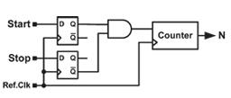
Fig.1: CounterbasedTDC
This architecture offers a wide measurement range and simple hardware implementation; however, its timing resolutionislimitedbytheclockperiod.
The design is described using Verilog HDL and simulated using Vivado to verify the counting operation and timing behavior.
To achieve finer time resolution, a buffer delay line based TDC is implemented. In this approach, a series of delay elements such as buffers or inverters are connected in sequencetoformadelaychain[2].Eachstageintroducesa smallpropagationdelay.Oncethestartsignalisapplied,it begins traveling through a sequence of delay elements arrangedinachain.
Whenthestopsignalisdetected,thestatesofalldelaystages aresampledatthesameinstantusingflip-flopsorregisters. The captured outputs form a pattern known as a thermometercode,whichindicateshowfarthesignal has propagatedthroughthedelayline.Thecountofactivestages (logic ‘1’) is converted into its equivalent binary representationtoobtainthefinemeasurement.
Thefinetimeintervalisdeterminedas:
Tfine =Nones ×Tdelay
Here,
Nones =Numberof1’sinthermometercode
Tdelay=Propagationdelayofonebufferstage
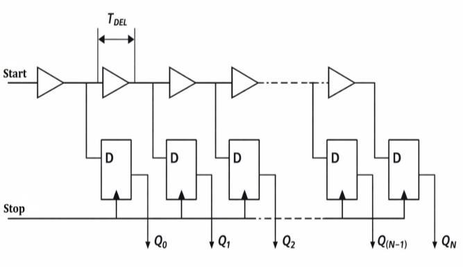
Fig.2: BufferdelaylineTDC
The design is described using Verilog HDL and simulated usingVivadotoverifythepropagationbehaviorofthedelay and generation of the thermometer code. This method provideshightimeresolution,typicallyinthepicosecondor sub-nanosecondrange.
Intheproposeddesign,bothcoarseandfinemeasurement techniquesarecombinedtoformahybridTDCarchitecture [4] The coarse measurement stage determines the time intervalbycountingcompleteclockcyclesbetweenthestart andstopevents.Atthesametime,thedelaylinestructure measuresthefractionalportionofthetimeintervalwithina singleclockcycle.
Duringoperation:
1. Thecounterbeginscountingclockcyclesafterthe startsignalisdetected
2. The delay chain monitors the signal progression within a single clock cycle to capture fine timing information.
3. Atthemomentthestopsignalisreceived,boththe counteroutputanddelay-linestatesarerecorded together.
Thetotalmeasuredtimeintervalisobtainedbycombining thecoarseandfinemeasurementsas:
Volume: 13 Issue: 03 | Mar 2026 www.irjet.net p-ISSN: 2395-0072 © 2026, IRJET | Impact Factor value: 8.315 | ISO 9001:2008
International Research Journal of Engineering and Technology (IRJET) e-ISSN: 2395-0056
Volume: 13 Issue: 03 | Mar 2026 www.irjet.net p-ISSN: 2395-0072
total =(Ccoarse×Tclk)+(Cfine×Tdelay)
Here,
Ccoarse =Numberofclockcycles(N)
Cfine=Numberof1’sinthermometercode(Nones)
Tclk=Clockperiod(e.g.,10ns=10,000ps)
Tdelay=Propagationdelayofonebufferstage(e.g.,100ps)
Thishybridarchitectureimprovesmeasurementaccuracyby combining thewiderange ofcounter-based measurement withthehighresolutionofdelay-lineinterpolation
The entire design is implemented using Verilog HDL and simulated in the Vivado environment, where waveform analysis is used to verify the functionality of both measurement stages. The simulation results showing the coarse count, thermometer code, and fine count are presentedintheresultssection
2.4 Power Optimization Using Flip-Flop Based Clock Gating
Although hybrid TDC architectures provide improved measurementresolution,theymayconsumehigherpower due to continuous switching activity in the clock network and delay line circuitry. To address this issue, a flip-flop basedclockgatingtechniqueisintroduced.
In this approach, the system clock is controlled using a gatingcircuitconsistingofanANDgateandaflip-flopbased enablesignal.TheclockisallowedtopropagatetotheTDC circuitry only when the measurement process is active. Whenthesystemremainsidle,theclocksignalisdisabled, preventingunnecessaryswitchingactivity.
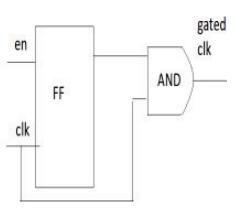
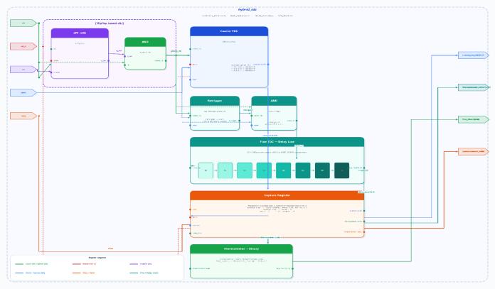
Byreducingredundantclocktransitions,theproposedclock gating mechanism significantly lowers dynamic power consumptionwhilemaintainingthefunctionalbehaviorand timingcharacteristicsoftheTDCsystem.
The simulation waveforms, schematic and various parametersofTDCarchitectureareshownbelow.
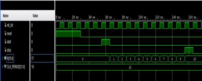
The waveform illustrates the working behavior of the counter-based TDC during coarse time measurement. The ref_clksignalprovidesthereferenceclockwithaperiodof 10 ns. When the start signal becomes active, the counter begins incrementing on each rising edge of the clock. The countervalueincreasessequentiallyfrom1to10untilthe stopsignaloccurs.Sincethecounterrecords10clockcycles, themeasuredtimeintervaliscalculatedasT=10×10ns= 100ns.Thisconfirmsthatthecounter-basedTDCcorrectly measures the time difference between the start and stop signals.
International Research Journal of Engineering and Technology (IRJET) e-ISSN: 2395-0056
Volume: 13 Issue: 03 | Mar 2026 www.irjet.net p-ISSN: 2395-0072
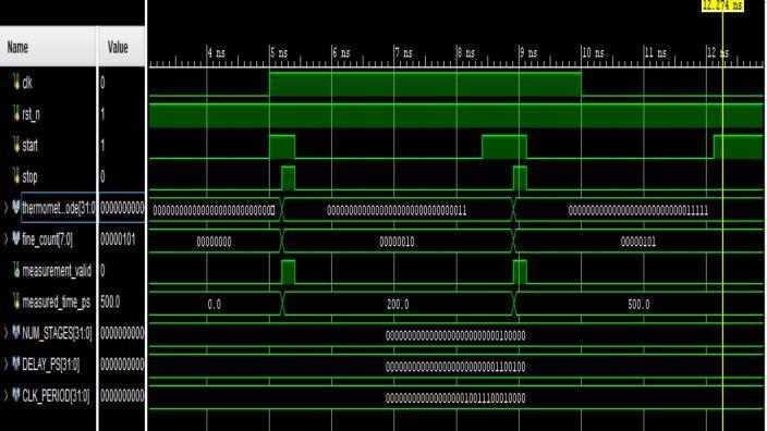
Thewaveformillustratesthefinetimemeasurementusinga bufferdelayline.Whenthestartsignalisapplied,thesignal propagatesthroughmultipledelaystages,eachintroducinga delayofapproximately100ps
At the arrival of the stop signal, for example, the thermometercodeshowsfive1’sproducingafinecountof5 Therefore,themeasuredfinetimeintervalis 5×100ps= 500 ps, confirming the correct operation of the delay-line basedTDC
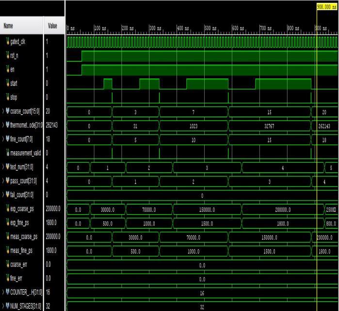
ThewaveformillustratestheoperationofthehybridTimeto-Digital Converter that combines coarse counter measurement and fine delay-line interpolation. When the start signal becomes active, the coarse counter begins countingtheclockcyclesofthegatedclock,whilethedelay linemeasuresthefractionalportionoftheinterval.
Forexample,thecoarsecounterrecordsvaluessuchas3,7, 15,and20clockcycles,correspondingto30ns,70ns,150 ns, and 200 ns respectively for a 10 ns clock period. The
delaylinesimultaneouslyproducesfinecountssuchas5,10, 15,and18,representing500ps,1000ps,1500ps,and1800 pswitha100psdelayperstage.Thetotalmeasuredtimeis obtained by combining the coarse and fine values, confirmingcorrecthybridTDCfunctionality.
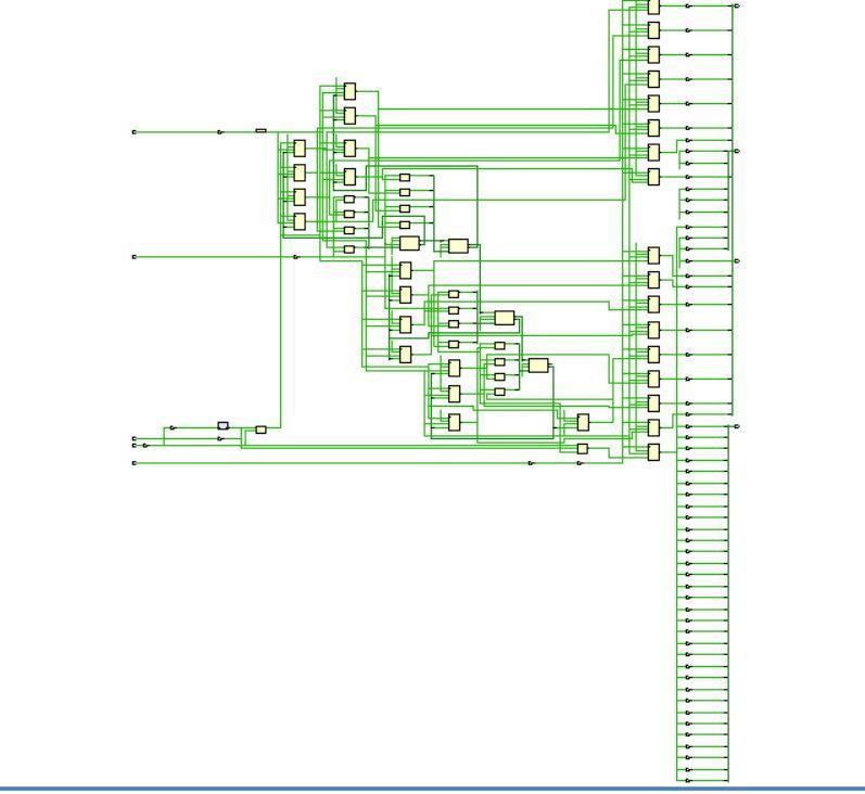
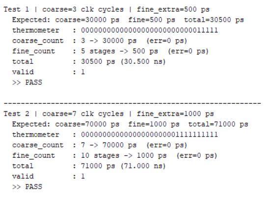
Fig.9: SchematicofHybridTDC
International Research Journal of Engineering and Technology (IRJET) e-ISSN: 2395-0056
Volume: 13 Issue: 03 | Mar 2026 www.irjet.net p-ISSN: 2395-0072
PowerofHybridTDC
AreaanddelayofHybridTDC


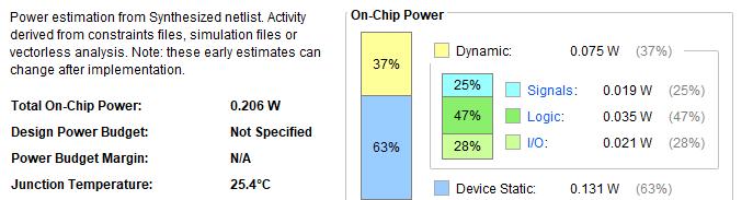
Fig.12: PowerofHybridTDCwithflipflopbasedclock gating
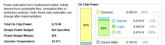
Thesynthesisresultsclearlyindicatethattheimplemented clock gating technique significantly improves power efficiency. Before optimization, the synthesized design consumed a total on-chip power of 8.76 W, where the dynamicpowercontributed8.595W(98%) andthestatic powerwas0.165W(2%).Afterapplyingtheflip-flopbased clockgatingtechnique,thetotalon-chippowersignificantly decreasedto0.206W.Intheoptimizeddesign,thedynamic powerreducedto0.075W,whilethestaticpowerbecame 0.131W.Thisreductionoccursbecausetheclockisenabled only during active measurement periods, preventing unnecessaryswitchinginidleconditions.
Overall,theproposedoptimizationreducesthetotalpower from 8.76 W to 0.206 W, which corresponds to approximately97.6%reductioninpowerconsumptionwhile maintaining the same functional operation and timing performanceofthehybridTDCsystem.
Table 1: Comparisonofparametervalues
Area[LUT’s] 18 19
In this work, a hybrid Time-to-Digital Converter (TDC) architecture has been designed and implemented by combiningacounter-basedcoarsemeasurementstagewith abufferdelaylinebasedfinemeasurementstage.Thecoarse measurementstagedeterminesthetimeintervalbycounting the clock cycles between the start and stop events, which allowsthesystemtomeasurelargetimeintervals.However, thetimingresolutionofthismethodislimitedbytheclock period. To improve resolution, a delay-line structure is utilizedtocapturefinetimingvariationswithinasingleclock cycle.
By combining both approaches, the hybrid architecture provides improved timing resolution while maintaining a wide measurement range. The proposed design was implemented using Verilog HDL and simulated using the Vivadodesignenvironment.Simulationresultsverifiedthe correct operation of the coarse counter, delay-line stages, andhybridmeasurementmechanism.
Although the hybrid architecture improves measurement accuracy,itincreasesswitchingactivityintheclocknetwork, whichresultsinhigherpowerconsumption.Toaddressthis issue, a flip-flop based clock gating technique was incorporatedintothedesign.Theclock gatingmechanism enablestheclockonlyduringactivemeasurementperiods and disables it when the circuit is idle. As a result, unnecessary switching activity is reduced and dynamic powerconsumptionissignificantlylowered. Parameter
International Research Journal of Engineering and Technology (IRJET) e-ISSN: 2395-0056
Experimentalresultsshowthattheproposedoptimization reducespowerconsumptionfromapproximately8.76Wto 0.206 W without affecting the functional performance or timingcharacteristicsofthesystem.Therefore,theproposed hybridTDCwithclockgatingprovidesanefficientsolution for high-resolution and low-power time interval measurementapplications.
[1] H. Xia, X. Yu, J. Zhang, and G. Cao, “A review of advancementsandtrendsintime-to-digitalconverters basedonFPGA,”IEEETransactionsonInstrumentation andMeasurement,vol.73,pp.1–25,2024
[2] Z. Soni, A. Patel, D. K. Panda, and A. B. Sarbadhikari, “Comparativestudyofdelaylinebasedtime-to-digital converterusingFPGA,”InternationalResearchJournal ofEngineeringandTechnology(IRJET),vol.4,no.9,pp. 1169–1175,Sep.2017.
[3] G. W. Roberts and M. Ali-Bakhshian, “A brief introduction to time-to-digital and digital-to-time converters,”IEEETransactionsonCircuitsandSystems II:ExpressBriefs,vol.57,no.3,pp.153–157,Mar.2010
[4] R. Machado, J. Cabral, and F. S. Alves, “Recent developmentsandchallengesinFPGA-basedtime-todigital converters,” IEEE Transactions on InstrumentationandMeasurement,vol.68,no.11,pp. 4205–4218,Nov.2019.
[5] B.K.Swann,B.J.Blalock,L.G.Clonts,D.M.Binkley,J.M. Rochelle,E.Breeding,andK.M.Baldwin,“100-pstimeresolutionCMOStime-todigitalconverterforpositron emission tomography imaging applications,” IEEE J. Solid-StateCircuits,vol.39,no.11,pp.1839–1852,Nov. 2004.
[6] M.Fahim,A.S.Elwakil,andS.Mirabbasi,“ALow-Power High-ResolutionTime-to-DigitalConverterUsingTime Amplification,” IEEE Transactions on Circuits and SystemsII,2015.
[7] Dehghani,M.Saneei,andA.Mahani,“AHigh-Resolution Time-to-Digital Converter Using a Three-Level Resolution,”InternationalJournalofElectronics,2014.
[8] P. Dudek, S. Szczepański, and J. V. Hatfield, “A highresolution CMOS time-to-digital converter,” IEEE JournalofSolid-StateCircuits,2000.
[9] J.Wu,“Severalkeyissuesonimplementingdelayline based TDCs using FPGAs,” IEEE Transactions on NuclearScience,vol.57,no.3,pp.1543–1548,2010.
[10] R. Szplet, A. Czuba, and J. Kalisz, “Subpicosecond resolutiontime-to-digitalconverter,”IEEETransactions onInstrumentationandMeasurement,2010.
[11] M.LeeandA.A.Abidi,“A9b,1.25psresolutioncoarsefine time-to-digital converter in 90 nm CMOS,” IEEE JournalofSolid-StateCircuits,2008.
[12] Niclass,M.Sergio,andE.Charbon,“A100-psresolution CMOStime-to-digitalconverter,”IEEEJournalofSolidStateCircuits,2008.
Volume: 13 Issue: 03 | Mar 2026 www.irjet.net p-ISSN: 2395-0072 © 2026, IRJET | Impact Factor value: 8.315 | ISO 9001:2008 Certified Journal | Page1125