International Research Journal of Engineering and Technology (IRJET) e ISSN: 2395 0056

Volume: 09 Issue: 06 | Jun 2022 www.irjet.net p ISSN: 2395 0072

International Research Journal of Engineering and Technology (IRJET) e ISSN: 2395 0056
Volume: 09 Issue: 06 | Jun 2022 www.irjet.net p ISSN: 2395 0072
1Assistant Professor/EEE, K L N College of Engineering, Pottapalayam, Tamilnadu, India 2Professor/EEE, K L N College of Engineering, Pottapalayam, Tamilnadu, India 3 4 5 UG Scholars, K L N College of Engineering, Pottapalayam, Tamilnadu, India ***
Abstract - DC DC conversion is the central stem of power electronics and is advancing quickly Many newtopologies are still created every year. The most common design of DC DC converters is typically, a converter with high gain, in orderto increase the output voltage of the photovoltaic and to obtain a high conversion efficiency. The SEPICconverter is a converter topology which is used to provide a regulated output voltage from an input voltage that varies above and below the output voltage. However, comparing to conventional DC DC converter topologies, SEPIC converters can increase by 5 times of the input voltage. A SEPIC converter of type is designed and evaluated in this paper. Conventional DC DC SEPIC Buck Boost type converter is utilized forindustrial applications like DC motor control, LED light drives, etc., SEPIC converter is much suitable for high voltage applications. The DC DC SEPICconverter is controlled to extract the maximum power from a Source to charge (or) control the Load. The SEPIC converter will operate in Continuous Conduction Mode in order to increase the Efficiency of the Converter. Analysis is made for both Open Loop and Closed Loop of theConverter in MATLAB/Simulink
Key Words: Converter, SEPIC Efficiency, High-Voltage Application, Pulse Width Modulation, CCM, DCM, BuckBoost, Closed loop.
These days, there are many purposes behind the advancementofelectricvehicles(EVs).Themostimportant reasons are increasing of fuel cost, lacking in energy resources and reduce the greenhouse gas emission. The advantagesofusingtheEVscanbestatedas,beingasource ofthecleanenergy,havinghighefficiencywhencomparedto theconventionalvehiclesandproducinglessnoisethanthe conventional vehicles. The EVs that are widely used in worldwide,canbeeitherahybridEVsorbatteryEV's.Many researches had proposed many converters for charging & controllingapplicationsofEV.Someofthemarelistedbelow;
PiyushChoudharyandSomNathMahendrahasproposeda DC DCcukconverter[1]forsolarphotovoltaicarraywhich
hasaninductorcurrentof20%and50%more.Anefficiency of 90% and more is achieved. They both has made the calculationsandanalysis,inCCMmodeoperation,transfer function,statespaceanalysis,simulationofcukconverterare done.
DanilaShirly.A.R,SudhilayaM,PriyadharshiniY,ShamniJ and Poorani J has proposed a paper which predominantly focuses on the design and implementation of efficient landsmanDC DCconverter[3]withpowerlossminimization using particle swarm optimization (PSO) a hybrid soft computingtechnique.But,theboostingofoutputvoltageis only2timesoftheinputvoltage.
P.Ramesh Babu, S.Ram Prasath and R.Kiruthika has putforthapaperofsimulationandperformanceanalysisof CCM zeta converter [2] with PID controller. They have designed, analyzed, simulated, close loop, continuous conduction code of zeta converter in their paper. The converter works in continuous current mode (CCM) as it were.But,Theboostingofinputvoltageisn'tunreasonably much high. In any case, the converter has lower Output voltageRippleandhashighproductivity.
AliaM.Khatab,Mostafa I.MareiandHadiM.Elhelwhas proposeda paperofanelectricvehiclebatterycharger[4] based on zeta converter fed from a PV array. This paper proposesabatterychargerforanelectricvehicle(EV)inview ofzetaconverter.Theperturbandobserve(P&O)maximum powerpointTracking(MPPT)techniqueisusedtoobtainthe maximum power from the PV array. The proposed P&O techniqueisusedforgeneratingthedutycycleforthezeta converterisworkingproperly.ButTheoutputcurrenthas highripple.
H.Suryoatmojo,I.Dilianto,Suwito,R.Mardiyanto,E.Setijadi and D.C.Riawan have proposed a paper named design and analysis of high gain modified SEPIC converter for photovoltaic applications. The proposed converter has the advantage of the SEPIC converter, like consistent input current.Theproposedcircuitstructurelikewiseworksonthe elements, like high voltage gain and high conversion
International Research Journal of Engineering and Technology (IRJET) e ISSN: 2395 0056
Volume: 09 Issue: 06 | Jun 2022 www.irjet.net p ISSN: 2395 0072
productivity. The proposed converter only applicable for 100W devices only. This converter has 2 more storage elementscomparingtoproposedconverter.
FaizanHameed,KhalidIqbalbothhasProposedapaperof ZETAConverterbasedchargecontrollerforefficientuseof solar energy in street lighting system. Purpose of circuit’s designedistochargethebatterybetweenupperandlower voltagelimitsinadditiontocontinuouscheckingthestatusof battery charge to add or release current accordingly. This proposed converter only applicable for low power rated devicesonly.Theconverterhashighoutputcurrentripple. Principal contrast between the strategy utilized in the proposedsystemanddifferentmethodsutilizedinthepastis thatZETAconverteritselfwillgoaboutaschargeregulator what'smorewiththis,specificpropertiesofZETAconverter willbeusedtooptimizestreetlightingsystemtoreducethe powerlossesandcost.
SurajS,JijeshJJ,SarunSomanhasproposedaconverter analysis of dual phase dual stage boost converter for photovoltaic applications. The converter discussed in this paperisderivedbycombiningtheconceptofinterleavingand cascadingofboostconverters.Theconverterisintendedfora powerratingof200Wwithyieldvoltageof192Vforaninput voltageof12Vgotfromphotovoltaicsourceatanexchanging frequencyof50KHz.Thisresultsexhibitthatthisconverter achievesapredominantperformanceoverotherdc dcboost convertersbyofferingimprovedefficiencyandvoltagegain, whilehavinglowerinputcurrentripple.
SEPIC converter has a lot of advantages which can be summarized as follows, it has a simple design, which composesfromfourenergystorageelements;twoinductors andtwocapacitors.Theresultcurrentcanbeconstantand liberated from the ripples because of the presence of an inductor at the result side. Operating as a buck boost convertermeansthat,theSEPICconverterhastheabilityto increaseanddecreasetheoutputvoltagethaninputvoltage. Whencomparedtotheconventionalbuck boostconverter, theoutputvoltageisnotinverted.Ithaslittlesettlingtime, lowexchangingpressureandittendstobeassociatedwith highfrequencytransformers.
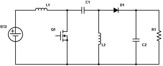
ThecircuitconfigurationoftheproposedDC DCconverteris showninfigure1.Itoperates inainputvoltageof16 24 V. The power circuit strategy ispresentedwithtwo inductors,twocapacitors,oneDIODEandoneMOSFETswitch operatingataswitchingfrequencyof 30kHz.
Theproposedconverterisdesignedfor300Wapplications. Theregulatedoutputvoltageandoutputcurrentwillbe60 Vand5Arespectively.
The design specifications of theproposed converter are shownin
TheequationtofindthedutycycleDis,
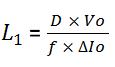
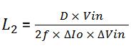
TheequationtodeterminetheinductorsL1andL2is,
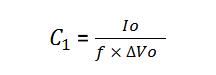
TheequationtodeterminethecapacitorC1is,
Where, △Io=2%ofoutputcurrent, △Vin=5%ofinputvoltage, △Vo=5%ofoutputvoltage
So,thesearethedesignequationofthisproposedconverter. Usingthisequationsthecomponentsvaluesarederived.
Table -1: DesignSpecificationofTheConverter
VALUES
SupplyVoltage(Vin) 16V 24V Inductor(L1) 540µH Inductor(L2) 2.7µH Capacitor(C1) 93µF Capacitor(C2) 4700µF
OutputPower(Po) 300W
Output Voltage (Vo) 60V
OutputCurrent(Io) 5A
Switchingfrequency(fs) 30kHz
International Research Journal of Engineering and Technology (IRJET) e ISSN: 2395 0056
Volume: 09 Issue: 06 | Jun 2022 www.irjet.net p ISSN: 2395 0072
Fig 2: OpenloopsimulationdiagramofDC DCSEPIC converter
Figure 2 shows the open loopsimulation diagram of the proposedconverter.Thishaspulsegeneratorwhichgivesthe gatepulsetotheMOSFETswitchofproposedconverter.The duty cycle of the switch controls the output voltage. So by varyingthedutycycle,Theoutputvoltagecanbevaried.
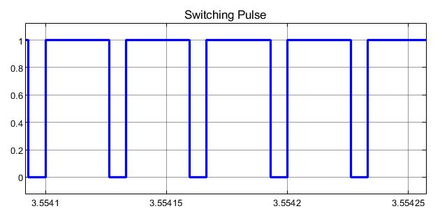
Fig 5:SwitchingPulseWaveformofDC DCSEPIC Converter
Figure5showstheswitchingpulsewaveformoftheproposed DC DC SEPIC converter which is generated by pulse generator. Here the switching frequency(fs) is 30KHz. The dutycycleofisgivenbythispulsegenerator.
4.2 Closed Loop Simulation of DC-DC SEPIC Converter using PI Controller
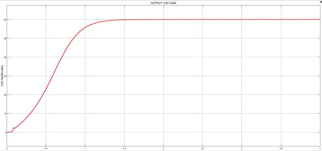
Fig 3:OutputvoltagewaveformofopenloopDC DCSEPIC converter
Figure3shows theoutputvoltagewaveformoftheDC DC SEPICconverterunderopenloop.Thedesiredoutputvoltage of60Visnotobtainedinopenloopcontrol,insteadanoutput voltageof51.5Visobtained.
Fig 6: ClosedLoopSimulationDiagramofDC DCSEPIC ConverterusingPIController
Figure 6 shows the closed loop simulation diagram of the proposedconverter.Inopenloop,theexpectedoutputsare notobtained.So,movingtoclosedloopsystem.Thiscircuit hasafeedbackcircuit,whichiscontrolledbyPIcontroller. ThePIcontrolleristhemostcommonlyusedinclosedloop systemsbecauseofitsperformanceintermsofsimplicity.It produces an error signal by comparing the desired output signalwiththeactualoutputsignal.
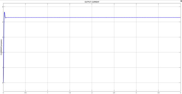
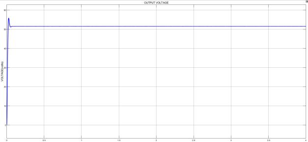
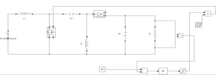
Fig 4:OutputcurrentwaveformofopenloopDC DCSEPIC converter
Figure4showstheoutputcurrentwaveformoftheDC DC SEPICconverterunderopenloop.Thedesiredoutputcurrent is5A.Butinopenloop4.5Aofcurrentisonlyobtained.
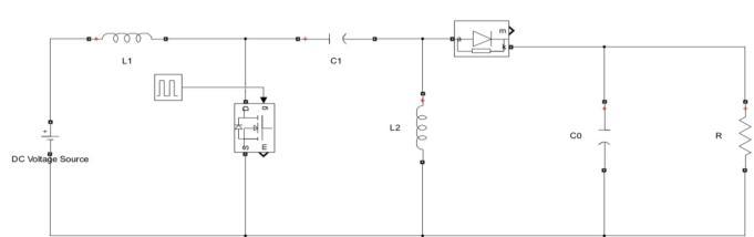
Fig 7:OutputVoltageWaveformofClosedloopDC DC SEPICConverter
Figure7shows theoutput voltagewaveformoftheDC DC SEPIC Converter under Closed loop. The desired output voltage of60Visobtainedat 1.5seconds. Then theoutput voltagebecomesstableandconstantinclosedloopsystem. TheallowableripplevoltageofDCconvertersis5%ofoutput
International Research Journal of Engineering and Technology (IRJET) e ISSN: 2395 0056
Volume: 09 Issue: 06 | Jun 2022 www.irjet.net p ISSN: 2395 0072
voltage.Inthisproposedconverter,itisveryminimumwhich lessthanits1%ofoutputvoltage.
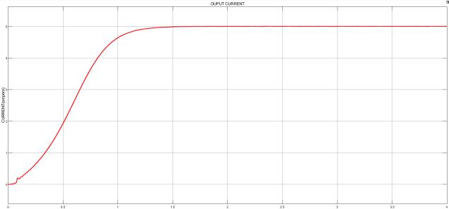
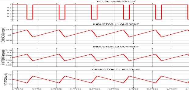
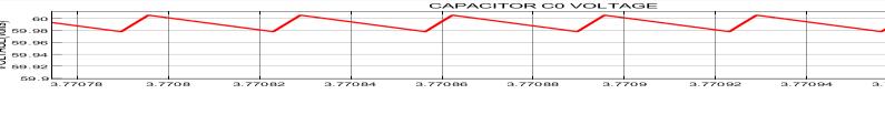
Table 2: Open loopanalysisofconstantinputvoltage variabledutycycle
Vin Iin Vout Iout D Efficiency
16 0.07851 3.201 0.2668 20 67.99%
16 0.2162 6.04 0.5033 30 87.87%
16 0.5661 9.807 0.8172 40 88.48%
16 1.285 15.04 1.253 50 91.65%
16 2.875 22.62 1.885 60 92.72%
Fig 8: OutputCurrentWaveformofClosedloopDC DC SEPICConverter
Figure8showstheoutputCurrentwaveformoftheDC DC SEPIC Converter under Closed loop. The desired output Current of 5A is obtained in Closed loop control. The allowable ripple current of DC converters is 2% of output current.Inthisproposedconverter,itisveryminimumwhich lessthanits0.5%ofoutputcurrent.Sobythis,theconverter isjustifiedasaripplefreeconverter.
16 6.782 34.52 2.876 70 91.49% 16 18.15 54.1 4.509 80 84.02%
Table.2 gives the analysis of constant input voltage and variable duty cycle under open loop condition. The input voltageiskeptconstant16Vthenvaryingthedutycycleby pulse generator the output voltage is varied. The output voltage is both less and greater than the input voltage correspondingtothedutycycle.Bythistable,theproposed converterachievethebothbuckandboostoperation.
Table 3: Closed loopanalysisofvariableinputvoltage constantoutputvoltage
Vin Iin Vout Iout Efficiency
16 22.97 60 5 84.58% 18 19.43 60 5 85.38% 20 16.98 60 5 87.48% 22 15.11 60 5 89.88% 24 13.61 60 5 91.18%
Fig 9: Waveforms of Switching pulse, InductorL1 Current, Inductor L2 Current, Capacitor C1 Voltage, Capacitor C2 Voltage under Closed loop
Figure 9 shows the waveforms of switching pulse, inductorL1current,inductorL2current,capacitorC1voltage, capacitor C2 voltage of DC DC SEPIC converter. When, MOSFET switch is turned ON, the inductor L1 and L2 are chargingandthecapacitorC1 andC2 aredischarging.When, MOSFET Switch is turned OFF, the inductorL1and L2are dischargingandthecapacitorC1 andC2 aregettingcharged. Thisproposedconverteroperatesin continuousconduction mode(CCM)whensimulatedunderclosedloop.
Table.3 gives the analysis of Variable Input Voltage and Constant Output Voltage under Closed loop. The input voltage is varied from 16 24V and the output reference voltage is 60V that is kept constant. By varying the input voltage, the efficiency of the proposed converter is also varied. There is a gradual increase in efficiency when the input voltage is increased gradually. The input current is reduced,asincreaseininputvoltage.
Table -4: Closed loopanalysisofconstantinputvoltage variableoutputvoltage
Vin Iin Vout Iout Efficiency
16 13.64 48 4 88.91%
16 17.83 54 4.501 84.34%
16 22.97 60 5 84.58% 16 29.28 66 5.5 77.09% 16 33.86 72 5.928 72.13%
International Research Journal of Engineering and Technology (IRJET) e ISSN: 2395 0056
Volume: 09 Issue: 06 | Jun 2022 www.irjet.net p ISSN: 2395 0072
Table.4 gives the analysis of constant input voltage and variableoutputvoltage.Theinputvoltageiskeptconstant and the output reference voltage is varied. The proposed converter is provide the expected output voltages. But, abovethedesignedoutputvoltage(60V)theefficiencyofthe converterisreduced.Theinputcurrentisalsoincreasedby increasingtheoutputreferencevoltage.
Table 5: Closed loopanalysisofconstantinputvoltage constantoutputvoltage variableLoad
Vin Iin Vout Iout Efficiency % of resistive load
16 50.71 60 8.283 63.98% 60%
16 37.56 60 7.143 72.02% 70%
16 30.82 60 6.25 76.68% 80%
16 25.76 60 6.00 78.89% 90%
16 22.97 60 5 84.25% 100%
16 19 60 4.287 84.78% 120%
16 16.7 60 3.837 85.40% 130%
16 15.33 60 3.572 86.35% 140%
Table .5 gives the analysis of closed loop constant input voltageandconstantoutputvoltagewithvariableresistive load. The input voltage and output voltage both are kept constant. The resistive load is only varied. The full load resistance value is 12Ω. The converter is also tested in overloadedcondition.Hereupto140%offullloadistested, whichis16.8Ω.Theconverterworksproperlyandgivesthe expected output voltage and efficiency is also slightly increased.
Inthispaper,theDesign, AnalysisandSimulationofDC DC SEPIC Converterhave been carried out for (16 22V) input and 60V output. Both open loop and closed loop analysis have been done for the designedconverter. The proposed converter not able to achieve the expected voltage and current in open loop system. So, moving to closed loop system.Theclosedloopsystemgivestherequiredvoltage (60V) and current (5A). The efficiency of the proposed converter is 85%. By taking varies analysis, the proposed converter can able to operate in both buck and boost operation.Theproposedconvertercanabletodobothstep upandstepdowntheinputvoltage.TheProposedconverter operates in Continuous Conduction Mode (CCM). The outputCurrenthas lowrippleand Thisconverterhashigh Efficiency.
[1] PiyushChoudharyandSomNathMahendra"Feedback controlandsimulationofDC DCCukconverterforsolar photovoltaic array" 2016 IEEE Uttar Pradesh Section International Conference on Electrical,Computer and Electronics Engineering (UPCON) Indian Institute of Technology(BanarasHinduUniversity)Varanasi,India, Dec9 11,2016.
[2]P.RameshBabu, S.RamPrasath and R.Kiruthika "Simulation and Performance Analysis of CCM Zeta Converter with PID Controller" 2015 International Conference on Circuit, Power and Computing Technologies[ICCPCT].
[3]DanilaShirly.A.R,SudhilayaM,PriyadharshiniY,ShamniJ and Poorani J " Improving Efficiency and Power Loss Minimization in Landsman DC DC Converter using ParticleSwarmOptimizationTechnique(PSO)"20212nd International Conference for Emerging Technology (INCET)Belgaum,India.May21 23,2021.
[4]AliaM.Khatab,MostafaI.MareiandHadiM.Elhelw"An Electric Vehicle Battery Charger Based on Zeta Converter Fed froma PV Array" 978 1 5386 5186 5/18/$31.00©2018IEEE.
[5]H.Suryoatmojo, I.Dilianto, Suwito, R.Mardiyanto, E.SetijadiandD.C.Riawan."DesignandAnalysisofHigh Gain Modified SEPIC Converter for Photovoltaic Applications". 2018 IEEE International Conference on Innovative Research and Development (ICIRD) 11 12 May2018,BangkokThailand.
[6] Faizan Hameed, Khalid Iqbal "ZETA Converter based charge controller for efficient use of solar energy in streetlightingsystem".InternationalJournalofAdvanced Research in Electrical,ElectronicsandInstrumentation Engineering,Vol.5,Issue6,June2016.
[7]E. Sanchis Kilders, A. Ferreres, Maset,Ejea,V.Esteve,J. Jordán, A. Garrigós, J. Calvente "Soft Switching Bidirectional Converter for Battery Discharging Charging".0 7803 9547 6/06/$20.00©2006IEEE.
[8]SurajS,JijeshJJ,SarunSoman "AnalysisofDualPhase Dual Stage Boost Converter for Photovoltaic Applications".InternationalJournalonAdvancedScience EngineeringandInformationTechnology·June2020.
[9]J.BarsanaBanu,M.BalasinghMoses"Modelling,control, andimplementationofthesoftswitchingdc dcconverter for battery charging /discharging applications". International Journal of Engineering and Technology · February2018.
International Research Journal of Engineering and Technology (IRJET) e ISSN: 2395 0056
[10]ManoharanPremkumar,UmashankarSubramaniam , Hassan Haes Alhelou and Pierluigi Siano “Design and Development of Non Isolated Modified SEPIC DC DC ConverterTopologyforHigh Step Up”Energies2020,13, 3960.
[11] ROHM Semiconductor “Calculation of Power Loss (Synchronous)“ No.AEK59 D1 0065 2 2016.10 Rev. 003.
[12] Praveen Kumar K , Purushothaman D S “ImplementationofModifiedSEPICConverterforStand AlonePVApplications”InternationalJournalofAdvanced ResearchinElectrical,ElectronicsandInstrumentation EngineeringVol.5,SpecialIssue5,March2016.
[13] Dr N Rathina Prabha, Dr J Gnanavadivel, K S Krishna Veni “Performance Investigation of Single Switch Dual Output DC DC SEPIC Converter for PV Applications” International Journal of Advanced Science and Technology(2020).
[14] Saurabh Kumar, Rajat Kumar, Navdeep Singh “PerformanceofClosedLoopSEPICConverterwithDC DC Converter for Solar Energy System” 2017 4th InternationalConferencePower,ControlandEmbedded Systems.
[15] Radha Kushwaha and Bhim Singh “ Interleaved LandsmanConverterFedEVBatteryChargerwithPower FactorCorrectionDOI10.1109/TIA.2020.2988174,IEEE.
[16] Rajan Kumar, Bhim Singh “Solar PV Array fed water pumping system using SEPIC Converter based BLDC Motor drive” 2014 18th National Power Systems Conference.
[17]NehaAdhikari,BhimSingh“Performanceevaluationof a low power solar PV energy system with SEPIC Converter”2011IEEENinthInternationalConferenceon PowerElectronicsandDriveSystems.
[18] R. Thangasankaran, Ms. S. Shanthini and Dr. S. Parthasarathy " Design And Analysis of AC DC Interleaved Negative Output Cuk Converter for Power Quality Enhancement". International Journal of EngineeringResearch&Technology(IJERT).
Volume: 09 Issue: 06 | Jun 2022 www.irjet.net p ISSN: 2395 0072 © 2022, IRJET | Impact Factor value: 7.529 | ISO 9001:2008 Certified Journal |