International Research Journal of Engineering and Technology (IRJET) e ISSN: 2395 0056

Volume: 09 Issue: 05 | May 2022 www.irjet.net p ISSN: 2395 0072

International Research Journal of Engineering and Technology (IRJET) e ISSN: 2395 0056
Volume: 09 Issue: 05 | May 2022 www.irjet.net p ISSN: 2395 0072
2
1Dept. Of E&IE, Siddaganga Institute of Technology (SIT), Tumkur, India.
2Associate Professor, Dept. Of E&IE, Siddaganga Institute of Technology (SIT), Tumkur, India. ***
Abstract - VLSI designers' major goal in today's technological environment is to optimize power, time delay, and area. Minimizing power consumption and time delay using traditional VLSI design approaches is a challenging work for designers. This can be avoided by transitioning to a new technological age, i.e., by shifting fromconventional CMOS design to Dynamic Style of design. This paper discusses about the implementation of 2x1 Mux using various Dynamic Logic Techniques and their comparative analysis are observed using Mentor Graphics Tools with 130nm Technology. This paper also discusses Schematic Design, Output Waveforms, andDelay Calculations for both Single gated and Double gated logics, as well as the various design techniques such as Conventional CMOS Logic, Pseudo NMOS Logic, Complementary CMOS (C2 MOS) Logic, Domino Logic, and Low Power Feed Through (LPFTL) Logic.
Key Words: VLSI Design, CMOS, Dynamic Gate, Pseudo NMOS,C2MOS,LPFTEL,MentorGraphics.
Since the previous decade, VLSI engineers have taken a consistentapproachtothedevelopmentofvariousdevices that consume less power, run at high speeds, and take up less space. Because low power portable gadgets are so importanttoconsumersintoday'ssociety.Designersfacea hurdleinbuildingadevicethatmeetsallofthecustomers' needs while considering all of these factors. Traditional design strategies are insufficient for creating an efficient system.Asaresult,variousadvanceddesigntechniquesare requiredtoprovideuserswithabetterexperience.
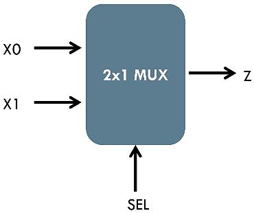
A multiplexer is a digital device that has N select lines, 2 powerNinputlines,andoneoutput.Ataninstantdepending uponthecontrolsignalattheselectlineonlyoneinputline is selected. Multiplexer is also known as a many to one digitalswitch.Asimple2x1Muxmoduleanditstruthtableis shownintheFig.1belowandTable1respectively.
Fig 1: GenericDiagram2×1Multiplexer. Table 1: TruthTableof2x1Multiplexer.
SEL X0 X1 Z 0 0 0 0 0 0 1 0 0 1 0 1 0 1 1 1 1 0 0 0 1 0 1 1 1 1 0 0 1 1 1 1
Atotaloftendifferentdesignstylesarebeingimplemented, simulated,andcomparedinthispaperwhichareCMOSlogic, COMSlogicwithDoubleGate,PseudoNMOSlogic,Pseudo NMOS logic with Double Gate, C2MOS logic, C2MOS logic withDoubleGate,Dominologic,DominologicwithDouble Gate. LP FTL logic, and LP FTL logic with Double Gate. All MultiplexersaredesignedusingFieldEffectTransistors.
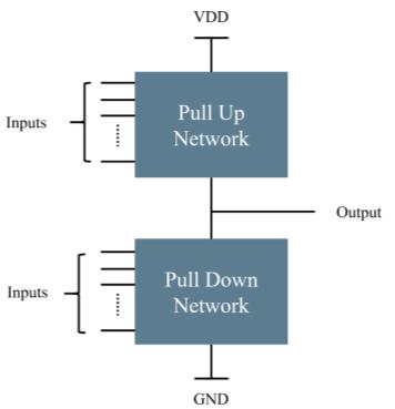
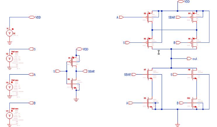
In conventional CMOS logic, two networks (Pull Up NetworkandPull DownNetwork)arecoupledatoneoutput node.PMOSdevicesmakeformaPull UpNetwork,whereas NMOSdevicesmakeupaPull DownNetwork.WhenthePull DownNetworkisturnedON,theoutputisconnectedtothe ground(Logic0),andwhenthePull UpNetworkisturned ON,theoutputisconnectedtotheVDD(Logic1).Ageneric
International Research Journal of Engineering and Technology (IRJET) e ISSN: 2395 0056
Volume: 09 Issue: 05 | May 2022 www.irjet.net p ISSN: 2395 0072
representationofconventionalCMOSlogicisasshowninFig. 2.
Analysis of power consumption and time delay are performedinmentorgraphics130nmtechnology.Fig.3and Fig.4representstheSchematicrepresentationofsinglegated anddoublegatedConventionalCMOSLogic2x1Multiplexer respectively.Powerconsumptionandtimedelayobservedby thisschematicdesignaretabulatedinTableIIunderresults section.
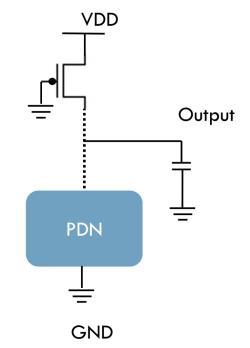
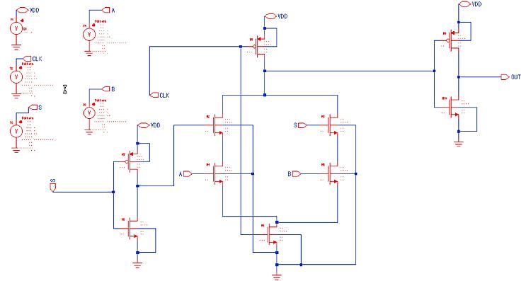
A Pseudo NMOS logic design also consists of Pull Up NetworkandPull DownNetworkconnectedatoutputnode. ButincaseofPseudoNMOSlogicPull UpNetworkisalwaysa PMOSdevicewhosegateterminalisconnectedground.And thePull DownNetworkremainssameasConventionalCMOS logic.A generic representation of PseudoNMOSlogic isas showninFig.5.
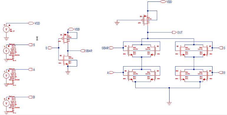
Compared to CMOSlogic Pseudo NMOSlogic consist of fewertransistors.Only(N+1)FETsarerequiredforNinput logic.SincethegroundedgateatPull UpNetwork,thepFET has been biased active. Schematic representation of single gatedanddoublegatedPseudoNMOSLogic2x1Multiplexer areasshowinFig.6andFig.7respectively.
Fig 2: ModulerepresentationofConventionalCMOS Logic.
Fig 5: ModulerepresentationofPseudoNMOSLogic.
Fig 3: SchematicrepresentationofConventionalCMOS Logic2x1Multiplexer.
Fig-6: PseudoNMOSLogicSchematicDiagramfor2×1 Multiplexer.
Fig 4: SchematicrepresentationofConventionalCMOS LogicDoubleGated2x1Multiplexer.
Fig 7: PseudoNMOSLogicSchematicDiagramfor DoubleGate2×1Multiplexer.
© 2022, IRJET | Impact Factor value: 7.529 | ISO 9001:2008 Certified Journal | Page2127
International Research Journal of Engineering and Technology (IRJET) e ISSN: 2395 0056
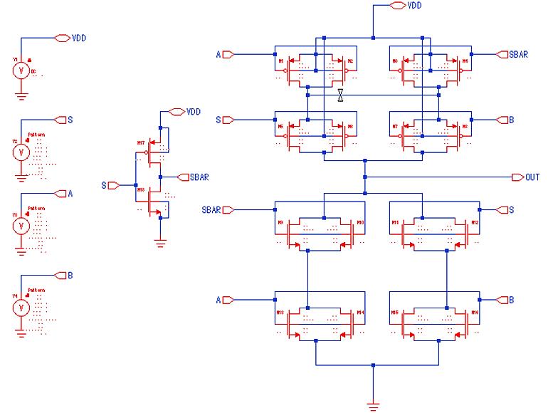
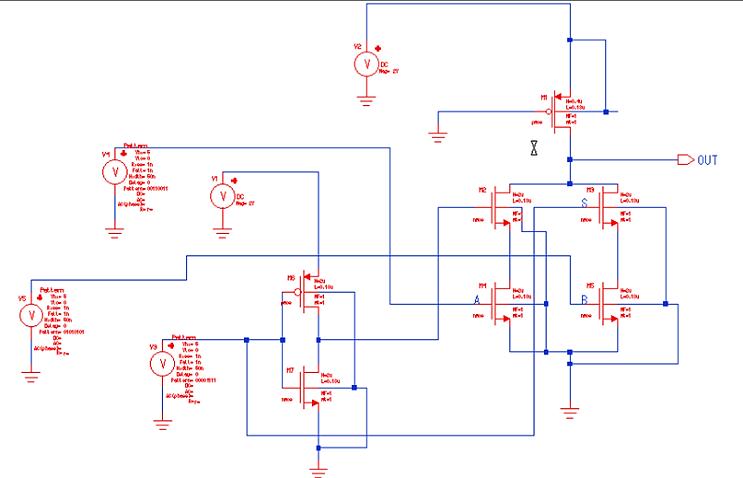
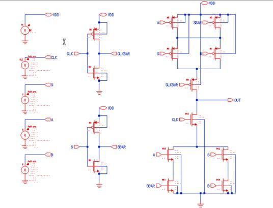
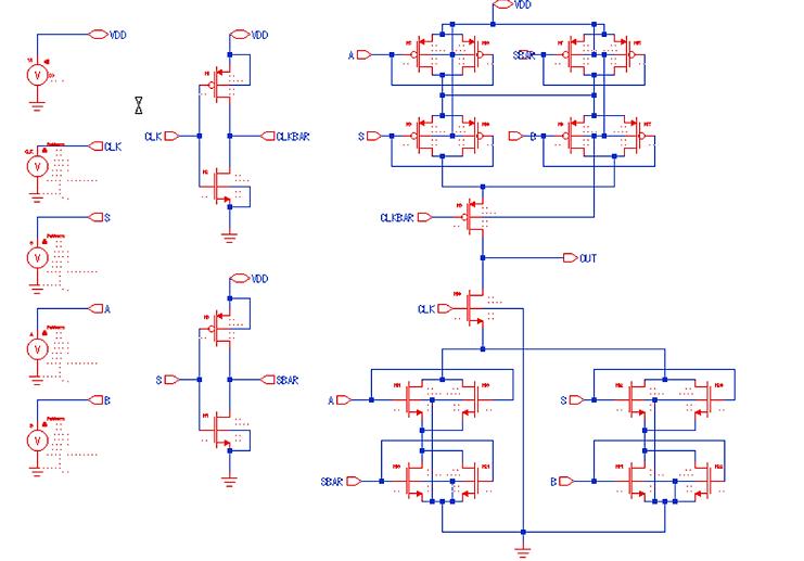
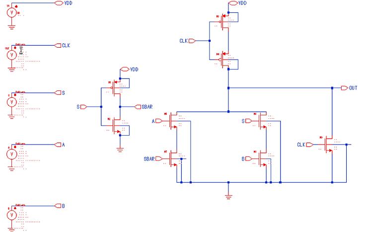
C2MOS(CSquareMOS)standsforClockedCMOSlogic. C2MOSlogicisessentiallyamodificationofstaticCMOSlogic, withanadditional PMOStransistorwhosegateterminalis connectedtotheComplimentedClocksignal(CLK_bar)and anNMOStransistorwhosegateterminalisconnectedtothe actual Clock signal (CLK). Like static CMOS logic Pull Up Networks are made up of PMOS transistors, whereas Pull DownNetworksaremadeupofNMOStransistors,CLK_bar and CLK are complementary clock signals that should preferablynotoverlap.Fig.8representsthebasicstructureof C2MOSlogic.
WhenCLK=1andCLK_bar=0bothMnandMptransistor areinONstate,sinceboththetransistorsareONthatimplies there is short circuit between Pull Up and Pull Down Network, hence current starts flowing which offers a low impedanceandthenetworkisnowreducedtostaticCMOS circuit. Depending up on the inputs circuit will generate outputeitherLogic1orLogic0.
Fig 10: C2MOSSchematicDiagramforDoublegate2×1 Multiplexer.
Domino logic is a design style that eliminates the cascading problem observed in dynamic CMOS logic. In a dominoCMOSlogic,adynamicCMOSlogichasbeencascaded withastaticCMOSinverter.AbasicstructureofDominologic isasshowninFig.11.
Fig 8: BasicStructureofC2MOSLogic.
When CLK=0 and CLK bar=1 Since both Mn and Mp transistors are turned OFF, the Pull Up and Pull Down Networksareseparatedfromtheoutputnode.Asa result, inputshavenoinfluenceontheoutputnode,whichisnowin ahigh impedancestate.UntilCLK=1,theoutputisstoredon thecapacitorCout.Schematicrepresentationofbothsingle gatedanddoublegatedC2MOSLogic2x1Multiplexerareas showinFig.9andFig.10respectively.
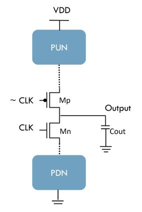
Fig 11: BasicStructureofDominoLogic. RegardlessoftheinputsinthePull DownNetwork,when CLK=0, pre charge transistor Mp is switched ON and evaluation transistor Mn is turned OFF. Cx capacitor pre chargestoVDDatnodeX,thusVx=VDD.ThisvalueofVxis nowappliedtoastaticCMOSinverter,resultinginVout=0vat theinverter'soutput.
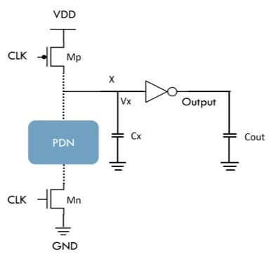
WhenCLK=1pre chargetransistorMpisswitchedOFF andevaluationtransistorMnisturnedON.NowifthePull DownNetwork isOFF,thenpre chargevoltageofVx=VDD willberetainedonCxcapacitorandVout=0vwillberetained onCout.IftheinputsaresuchthatPull DownNetworkisON, then Cx discharges to 0V via Pull Down Network and Mn transistor, therefore Vx=0V. Node X is conditionally discharged to ground based on Pull Down Network. A discharge of Cx results in a output of Vout=VDD (Logic 1). Schematic representation of both single gated and double gatedDominoLogic2x1MultiplexerareasshowinFig.12 andFig.13respectively.
Fig-9: C2MOSSchematicDiagramfor2×1Multiplexer.
Volume: 09 Issue: 05 | May 2022 www.irjet.net p ISSN: 2395 0072 © 2022, IRJET | Impact Factor value: 7.529 | ISO 9001:2008 Certified Journal |
International Research Journal of Engineering and Technology (IRJET) e ISSN: 2395 0056
chargestologichighorremainsatlogiclowdependingonthe inputs to the PDN block. Schematic representation of both singlegatedanddoublegatedLPFTL2x1Multiplexerareas showinFig.15andFig.16respectively.
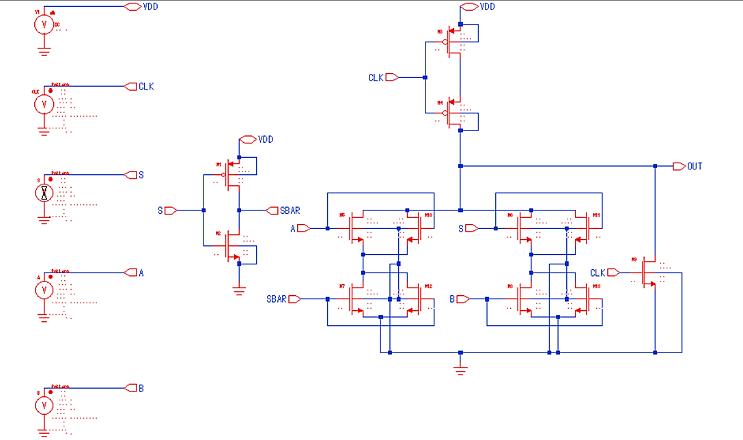
Fig 12: DominoLogicSchematicDiagramfor2×1 Multiplexer.
Fig 13: DominoLogicSchematicDiagramforDouble gate2×1Multiplexer.
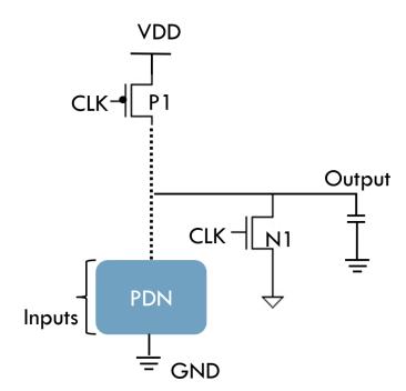
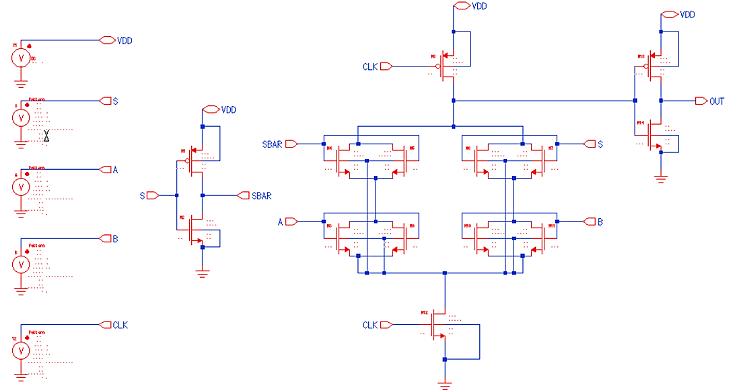
LPFTL was proposed to enhance domino logic performance.Dominologichadvariousrestrictions,which wereeliminatedinFTL.APull DownNetwork,aPMOSload transistorP1,andaresettransistorN1areusedincircuits design.InputsareappliedatthePull DownNetwork.Clock signal isconnectedtothegateinputsofloadtransistorP1 and reset transistor N1. A basic structure of LPFTL is as showninFig.14.
Fig 15: LPFTLSchematicDiagramfor2×1Multiplexer.
Representation.
Thecircuitoperatesintwostages:resetandevaluation. The clock is high during the reset phase, therefore load transistorP1isturnedOFFandresettransistorN1isturned ON, and the output is reset to a low logic level. The load transistor P1 is ON and the reset transistor N1 is OFF throughout the evaluation phase, and the output either
Fig 16: LPFTLSchematicDiagramforDoublegate2×1 Multiplexer.
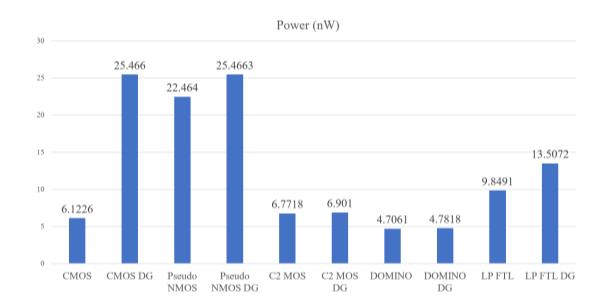
Inthissectionresultsofvariousdesignstylesarebeing simulated,observed,andtabulatedintheTableII.Also,the plotwithrespecttoPowerConsumptionandTimeDelayare depictedinFig.37&Fig.38.
Fig. 17, 19, 21, 23, 25, 27, 29, 31, 33, & 35 shows the output waveform for conventional CMOS, Double gated CMOS,PseudoNMOS,DoublegatedPseudoNMOS,C2MOS, DoublegatedC2MOS,Domino,DoublegatedDomino,LPFT,& DoublegatedLPFTlogic2X1Multiplexerrespectively.Fig.18, 20, 22, 24, 26, 28, 30, 32, 34, & 36 shows the Time delay observedforconventionalCMOS,DoublegatedCMOS,Pseudo NMOS, Double gated Pseudo NMOS, C2MOS, Double gated C2MOS,Domino,DoublegatedDomino,LPFT,&Doublegated LPFTlogic2X1Multiplexerrespectively.
Volume: 09 Issue: 05 | May 2022 www.irjet.net p ISSN: 2395 0072 © 2022, IRJET | Impact Factor value: 7.529 | ISO 9001:2008 Certified Journal |
International Research Journal of Engineering and Technology (IRJET) e ISSN: 2395 0056
Fig 17: OutputwaveformforconventionalCMOSlogic 2x1MUX.
Fig 21: OutputwaveformforPseudoNMOSlogic2x1 MUX.
Fig 18: TimedelayobservedforconventionalCMOS logic2x1MUX.
Fig-22: TimedelayobservedforPseudoNMOSlogic 2x1MUX.
Fig 19: OutputwaveformfordoublegatedCMOSlogic 2x1MUX
Fig 23: OutputwaveformfordoublegatedPseudo NMOSlogic2x1MUX.
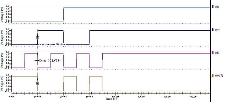
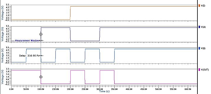
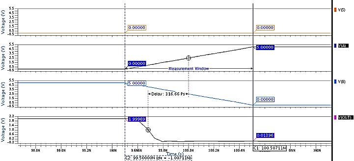
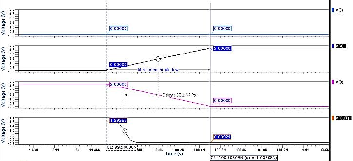
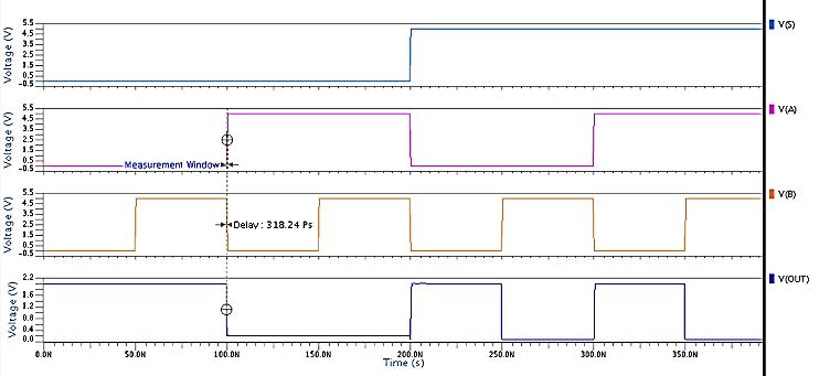
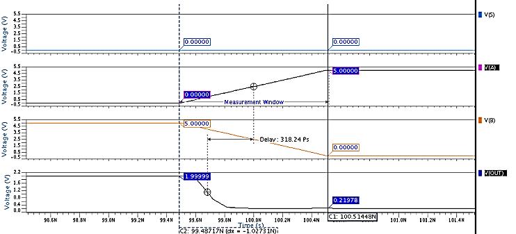
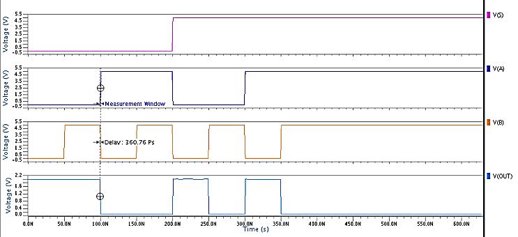
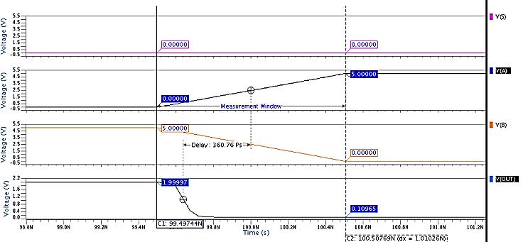
Fig 20: TimedelayobservedfordoublegatedCMOS logic2x1MUX.
Fig-24: TimedelayobservedfordoublegatedPseudo NMOSlogic2x1MUX.
Volume: 09 Issue: 05 | May 2022 www.irjet.net p ISSN: 2395 0072 © 2022, IRJET | Impact Factor value: 7.529 | ISO 9001:2008 Certified Journal |
International Research Journal of Engineering and Technology (IRJET) e ISSN: 2395 0056
Fig 25: OutputwaveformforC2MOSlogic2x1MUX
Fig 30: TimedelayobservedforDominologic2x1 MUX.
Fig 26: TimedelayobservedforC2MOSlogic2x1MUX.
Fig 31: OutputwaveformfordoublegatedDomino logic2x1MUX.
Fig 27: OutputwaveformfordoublegatedC2MOS logic2x1MUX.
Fig-32: TimedelayobservedfordoublegatedDomino logic2x1MUX.
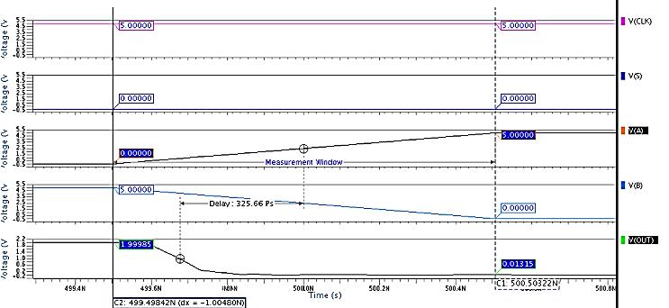
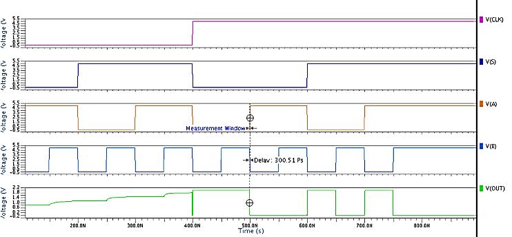
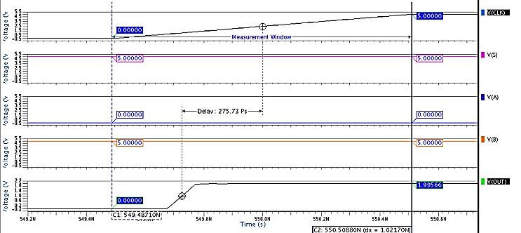
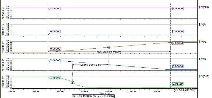
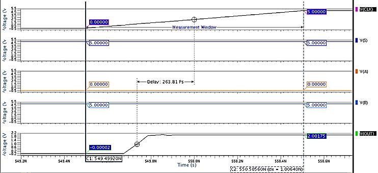
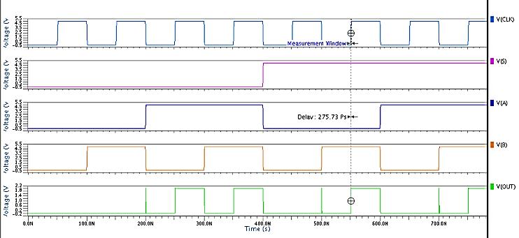
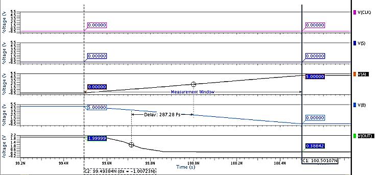
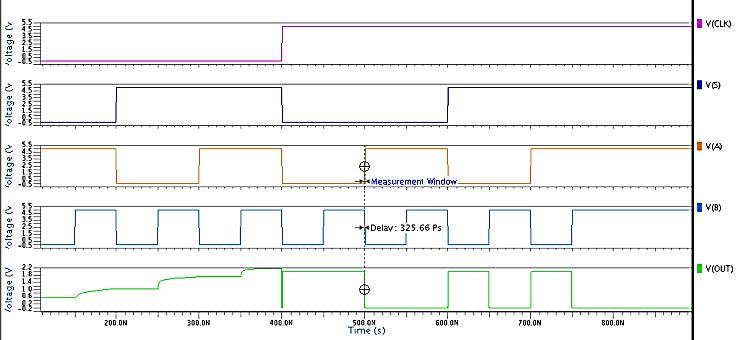
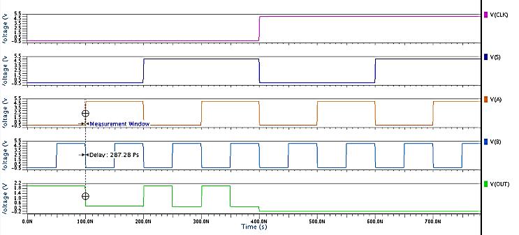
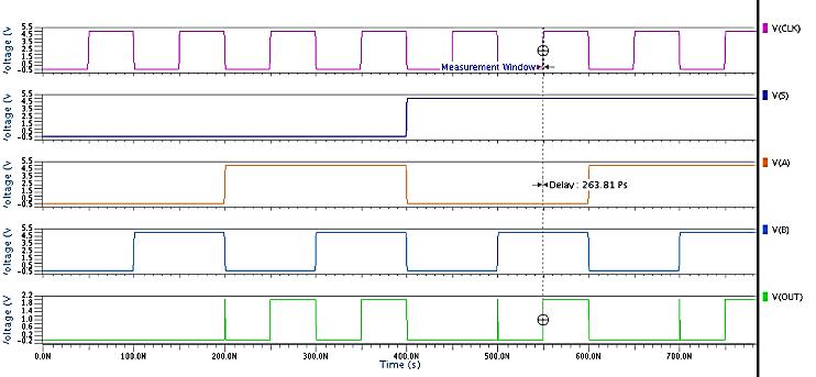
Fig 28: TimedelayobservedfordoublegatedC2MOS logic2x1MUX.
Fig 33: OutputwaveformforLPFTL2x1MUX.
Fig-29: OutputwaveformforDominologic2x1MUX.
Fig-34: TimedelayobservedforLPFTL2x1MUX.
Volume: 09 Issue: 05 | May 2022 www.irjet.net p ISSN: 2395 0072 © 2022, IRJET | Impact Factor value: 7.529 | ISO 9001:2008 Certified Journal |
International Research Journal of Engineering and Technology (IRJET) e ISSN: 2395 0056
Volume: 09 Issue: 05 | May 2022 www.irjet.net p ISSN: 2395 0072
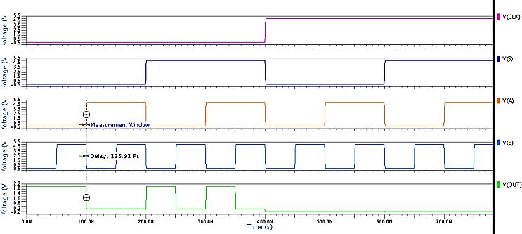
Fig-35: OutputwaveformfordoublegatedLPFTL2x1 MUX.
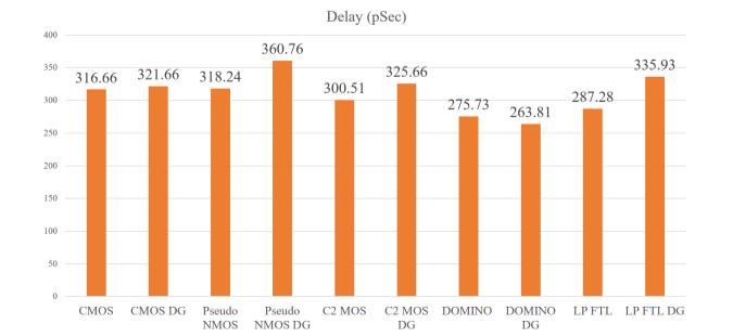
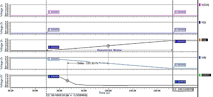
Fig-38: PlotofDelayin(pSec)fordifferentDesign Styles.
Implementation and Comparative Analysis of 2x1 Multiplexers Using Different Dynamic Logic Techniques is focusedondesigningandsimulationof2x1Multiplexerusing designtechniquessuchasConventionalCMOSLogic,Pseudo NMOSLogic,C2MOSLogic,DominoLogic,andLPFTLLogic usingMentorGraphis130nmtechnologyenvironmentandto analysetheeffectivelogicforimplementationof2x1Mux[1].
Fig 36: TimedelayobservedfordoublegatedLPFTL 2x1MUX.
Table 2: ObservedResultsOf2x1MultiplexerUsing DifferentDesignStyles
Sl.No. Design Power (nW) Delay (pSec) 1 CMOS 6.1226 316.66 2 CMOSDG 25.466 321.66 3 Pseudo NMOS 22.464 318.24 4 Pseudo NMOSDG 25.4663 360.76 5 C2MOS 6.7718 300.51 6 C2MOSDG 6.901 325.66 7 DOMINO 4.7061 275.73 8 DOMINODG 4.7818 263.81 9 LPFTL 9.8491 287.28 10 LPFTLDG 13.5072 335.93
Onsuccessfulsimulationofthedesign,resultsareplotted andtabulatedasshowninFig.37&Fig.38andTableII.By thisevidenceimplementationof2X1MuxusingDominoLogic yieldsLowPower(i.e.,4.7061nWinsinglegateddesignand 4.7818nWindoublegateddesign)andLessTimeDelay(i.e., 275.73pSecinsinglegateddesignand263.81pSecindouble gateddesign)whencomparedtootherDesignStyles.
[1] Mohit Vyas, Soumya Kanti Manna, Shyam Akashe, “DesignOfPowerEfficientMultiplexerUsingDualGate FinfetTechnology’’inproceedingofIEEEInternational ConferenceonCommunicationNetworks(ICCN),2015.
[2] AdityaWaingankar,AshaWaskar,YashVesvikar,Pratik Rathod,Mahalaxmi Palinge, “Logic Circuits Using Finfet:Comparative Analysis”, IJSRD ISSN:2321 0613, January2016.
[3] Neelam Bedwal, Renu Mehla, Archna Aggarwal, Bal Krishan, “Review on Alternatives for Conventional Transistor Technology”, International Journal of InnovativeResearchinComputerandCommunication EngineeringVol.4,Issue4,April2016.
[4] Ajay Kumar Dadori, Kavita Khare, T.K Gupta and R.P. Singh, “Leakage Power Reduction Technique by using FinFETTechnology”,November2015.
Fig-37: PlotofPowerinnWfordifferentDesignStyles.