International Research Journal of Engineering and Technology (IRJET)
e-ISSN: 2395-0056
Volume: 07 Issue: 08 | Aug 2020
p-ISSN: 2395-0072
www.irjet.net
Design and Verification of Peripheral Component Interconnect Express (PCIe) 3.0 K U Prasad Bhat1, Hrishikesh Ravish2, Anirudha V3, Prabhavathi P4, Kumaraswamy K V5 1,2,3Student,
Department of Electronics and Communication Engineering, BNMIT, Bengaluru, India Professor, Department of Electronics and Communication Engineering, BNMIT, Bengaluru, India 5Senior Technical Manager, Trident Techlabs Pvt. Ltd, Bengaluru, India ---------------------------------------------------------------------***---------------------------------------------------------------------4Associate
Abstract - PCIe (Peripheral Component Interconnect
Express), is a common motherboard interface standard for hard drives, SSDs, Ethernet and Wi-Fi connections as well as graphic cards with a computing system. PCIe provides multiple direct links that allows multiple devices to communicate with each other simultaneously. Many different versions of PCIe are developed in order to increase speed, bandwidth and data width. Hence, this project aims at developing a soft IP for PCIe 3.0 standard protocol. This had been modeled in Verilog HDL, simulated in Questa Simulator and synthesized in Precision RTL. PCIe 3.0 soft IP is developed as per FPGA design methodology with a clock frequency of 100 MHz, for Xilinx Vivado device. Equivalence Check was performed using FormalPro. Finally, the proposed design was checked for DO254 standard.
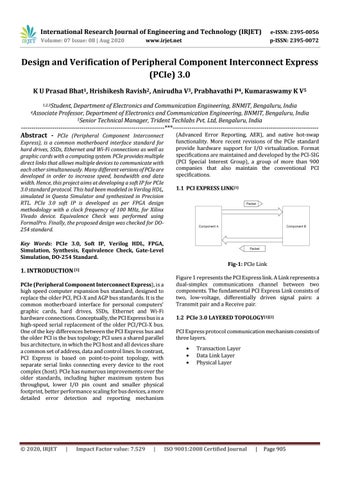
(Advanced Error Reporting, AER), and native hot-swap functionality. More recent revisions of the PCIe standard provide hardware support for I/O virtualization. Format specifications are maintained and developed by the PCI-SIG (PCI Special Interest Group), a group of more than 900 companies that also maintain the conventional PCI specifications. 1.1 PCI EXPRESS LINK[1]
Key Words: PCIe 3.0, Soft IP, Verilog HDL, FPGA, Simulation, Synthesis, Equivalence Check, Gate-Level Simulation, DO-254 Standard. Fig-1: PCIe Link
1. INTRODUCTION [1] PCIe (Peripheral Component Interconnect Express), is a high speed computer expansion bus standard, designed to replace the older PCI, PCI-X and AGP bus standards. It is the common motherboard interface for personal computers' graphic cards, hard drives, SSDs, Ethernet and Wi-Fi hardware connections. Conceptually, the PCI Express bus is a high-speed serial replacement of the older PCI/PCI-X bus. One of the key differences between the PCI Express bus and the older PCI is the bus topology; PCI uses a shared parallel bus architecture, in which the PCI host and all devices share a common set of address, data and control lines. In contrast, PCI Express is based on point-to-point topology, with separate serial links connecting every device to the root complex (host). PCIe has numerous improvements over the older standards, including higher maximum system bus throughput, lower I/O pin count and smaller physical footprint, better performance scaling for bus devices, a more detailed error detection and reporting mechanism
© 2020, IRJET
|
Impact Factor value: 7.529
|
Figure 1 represents the PCI Express link. A Link represents a dual-simplex communications channel between two components. The fundamental PCI Express Link consists of two, low-voltage, differentially driven signal pairs: a Transmit pair and a Receive pair. 1.2 PCIe 3.0 LAYERED TOPOLOGY[1][2] PCI Express protocol communication mechanism consists of three layers.
Transaction Layer Data Link Layer Physical Layer
ISO 9001:2008 Certified Journal
|
Page 905