10 minute read
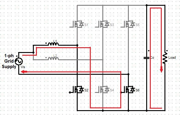
Fig.5: Totem pole Bridgeless Interleaved PFC circuit

International Research Journal of Engineering and Technology (IRJET) Volume: 07 Issue: 05 | May 2020 www.irjet.net e-ISSN: 2395-0056 p-ISSN: 2395-0072
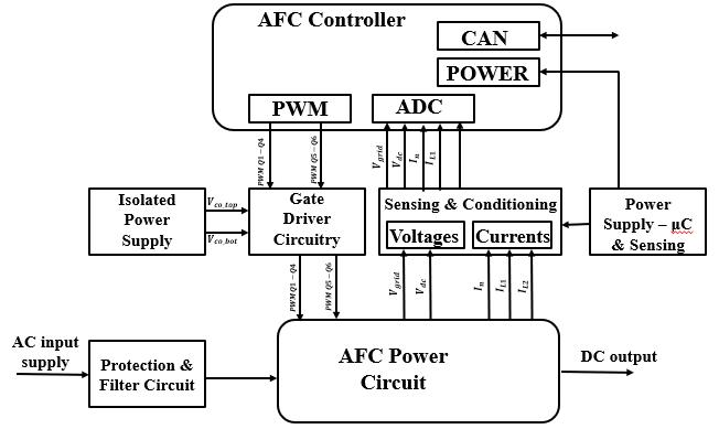
Voltage sensing and current sensing circuits sense the voltage level and currentlevelthrough the circuit and sends the signal to the control. Feedback signals from the temperature sensor, voltage and current measurement are loaded to the controller to monitor the health of the converter. The gating pulses to the switches in the circuit is given by the gate driver circuit. DC-link capacitance of the dc-to-ac converter reduces the ripples. Controller used is of automotive standards with required number of GPIOs, ADCs, and DACs. It constantly monitors the overall operation of the system. Microcontroller has the CAN port that communicates with the BMS (Battery Management System) using CAN controller. The microcontroller provides the necessary control signals to the driver circuit based on the BMS output.
Advertisement
2.1 Structure
Fig.4: Block Diagram of AFC Circuit.
1.5 Synchronous Rectification
In many applications diodes are used for rectification. Due to the diode conduction losses the overall power loss increases. The conduction losses are high in applications having higher current ratings. The equivalent forward voltage drop of MOSFET is very less compared to diode forward voltage drop. Hence, diodes are replaced by MOSFETs.
2. METHODOLOGY
Active Front –End Converter (AFC) is used to convert the grid supply (230 V, 1-ϕ, 50Hz) to DC (400 V) supply. The topology used is interleaved bridgeless totem – pole. The input current has large harmonic distortion, and it pollutes the grid. Hence PFC circuit is used to reduce the harmonics, and to meet the International standards of power factor and harmonic content requirement. The conventional PFC has the diodes that restricts the bidirectional action of the converter. In this topology, for two-way operation, transistors and diodes operation are included in the rectifier bridge. Hence, the name bridgeless PFC converter. This reduces the number of semiconductor and therefore the conduction losses. And the diodes are replaced by the slow switching Mosfet, enabling the flow of negative current. It now operates in Bidirectional mode. This also helps in synchronous rectification. Interleaving the totem – leg increases the overall efficiency of the converter and reduces the stress on the semiconductor switches. When compared to other mentioned topologies, the converter presented here has advantages of higher efficiency, smaller common mode noise, reduced ripples in ac input current, less reverse recovery current, a smaller no.of elements, simple control and simple gate drive design. Totem-pole bridge-less interleaved converter is as shown in the Fig.5 below. The
Power Switches ( to ) Filter Inductances ( ) DC link Capacitance ( )
critical components are:
Fig.5: Totem pole Bridgeless Interleaved PFC circuit.

2.3 Operation
Fig.5 shows the proposed bi-directional interleaved bridge-less totem pole PFC converter has six Mosfet. Two interleaved boost converters are reactor , switches & and reactor ,switches & which are operated with phase-shiftof 180⁰. In every phase, the top switch and the bottom switch operates complementing each otherwith a short dead-band period. Diodes for linerectification are substitutedwith twoswitches( and ) to be used for synchronous-rectification, this adds to the reductionin power losses and improving efficiency.
International Research Journal of Engineering and Technology (IRJET) Volume: 07 Issue: 05 | May 2020 www.irjet.net e-ISSN: 2395-0056 p-ISSN: 2395-0072
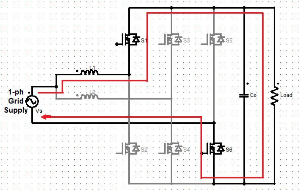
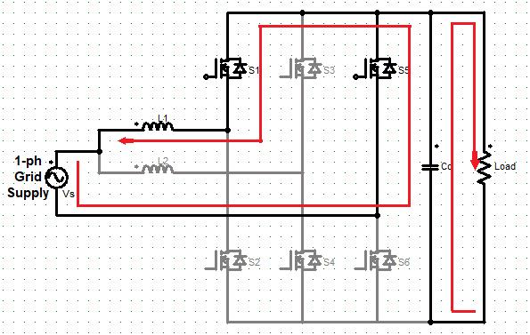
(a)
In the first half-period of supply, as seen in Fig.6(a), is closed, linking the positive side of grid supply to ground. And when is closed, the inductor
(b)
beforehand is on in order to avoid over-shoot in the current. After the deadband, is closed, seen in Fig.6(b), creatinga free-wheeling path forcurrentthrough inductor The ON time of is calculated by the duty cycle of boost converter, whereas the ON time of switch, is complimentary to . In the second half-period of supply, is closed,
is closed after is opened with a dead-band period, which allows synchronous-rectification and createsa free-wheeling path forcurrentthrough inductor,
gets charged.
Then is opened, a dead band periodis provided and dischargesthestoredenergy in thedc-linkcapacitor. as seenin Fig.6(d).
(d)
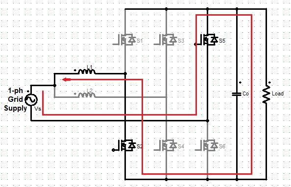
Fig.6: Different Modes of Operation of the Proposed Topology for G2V mode.
In the second half-period of supply, the ON time of switch, is calculated by dc-to-dc converter duty cycle. Switch and switch are used in the other phase, operatedwith phase-shiftof 180⁰in regards withswitches & The working of other boost interleaved phase is same as that of first phase, improving the effective operatingfrequency to double.
2.2 Controller
The controller structure of the AFC unit is as shown below in Fig.7. As seen in the Fig.7, there are three controllers or compensators (two current and one voltage) in the control loop. The AFC control loops design consists of the current-loop in the inner side, and the voltage-loop controller outer side. The inner current-loop controllers are fast controllers and the outer voltage-loop

(c)
controllers are slow controllers. joining the positive side of grid supply to dc-link. Then is closed, as seenin Fig.6(c), the source charges the reactor .
Fig.7: Control Diagram of AFC Circuit. Initially, the analog approach is followed for the compensator design, where the whole design is made in the continuous-time domain (s-domain). Finally, the parameters of the compensators are converted back into the discrete domain by using Bilinear transformation.
International Research Journal of Engineering and Technology (IRJET) Volume: 07 Issue: 05 | May 2020 www.irjet.net e-ISSN: 2395-0056 p-ISSN: 2395-0072
The other important hardware components in the AFC are: Driver circuit to provide gate-pulses to the power devices. Sensing circuits (current and voltage). EMI filters and protection circuit. Snubbers across the power devices (if required).
DESIGN OF CONVERTER
The most commonly used rectifier is the diode bridge rectifier. One of the major concerns about selecting the topology of the rectifier is the distortions in line current due to the source inductance. These harmonic components are responsible for the distortion of the voltage at the PCC and produce undesirable effects. Due to which power factor becomes worst. The reactors ( ) helps improve the power factor and the diodes and smoothing capacitors convert ac-to-dc.
The specifications of the AFC are as follows: InputACVoltage - 230 V Output DC Voltage - 400 V Output Power - 6.6 kW Line Frequency - 50 Hz Switching Frequency - 100 kHz Maximum DC Voltage - 600 V And consider, Efficiency - 93 % Power factor - 0.95
3.1 Inductor Calculation
Input Current is given as,
(1)
of rated current is considered as over current, then
ripple is considered in the maximum input current.
(2) Then with the current ripple, filter inductances are given by the equation as follows: (3)
Since, is varying. is maximum when
Hence, we can write
(4)
+20 % margin is assumed for the inductor from calculated value Hence, filter inductance value is RMS current rating of the inductor is given as,
(5)
A the
+30 % margin is assumed for the inductor value from the calculated value
A
A
Therefore, filter inductors of current rating A. is selected with
3.2 DC Link Capacitor Calculation
ripple is considered in the minimum output voltage. (6)
= 20 V DC link capacitor value using ripple voltage is given as,
(7)
DC link capacitor value using hold up time is given as,
Hold-up time is considered as 5 ms. (8)
International Research Journal of Engineering and Technology (IRJET) Volume: 07 Issue: 05 | May 2020 www.irjet.net e-ISSN: 2395-0056 p-ISSN: 2395-0072
Therefore, DC link capacitor of with voltage rating . is selected
4. Simulation and Results
The simulations of the on-board charger are carried out in MATLAB Simulink software. This section shows the simulations of the active front-end converter and the results obtained in the Simulink software.
4.1 Simulation Circuit
To validate the effectiveness of the designed controller and to check the performance of the AFC circuit, the selected AFC topology is simulated in MATLAB Simulink. Table.1 shows the components values considered for the MATLAB simulation of the circuit.
Table.1: Parameters of the AFC Circuit Considered for the MATLAB Simulations.
Parameters
AFC Inductors AFC DC-link Capacitors Switching Frequency Sampling Frequency
Bandwidth of Current Controller Bandwidth of Voltage Controller Grid Voltage Grid Frequency Power Rating of AFC Normal DC-link Voltage
Symbols
and C
Values
780 μH 3700 μF
100 kHz 100 kHz 10 kHz
5 Hz
230 V-rms 50 Hz 6600 W 450 V
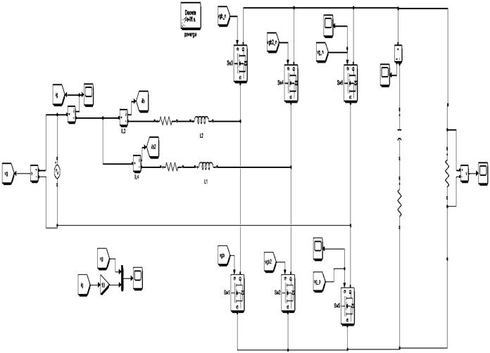
Fig.8 shows the AFC simulation circuit in grid-tovehicle mode. The input to the AFC circuit in Fig.8is 230 V, 50 Hz AC supply. the AFC converts AC supply to the form required by the batteries i.e., DC supply. Two reactors are used at the input to reduce the harmonics in the input supply and DC-link capacitor is used at load to decrease the ripples in the DC output of the AFC. The components values are designed in the previous section. The simulation results are used as the basis for hardware implementation. Fig.8: AFC Simulation Circuit in G2V Mode.
The practical AFC converter would always operate in CV mode, except during vehicle to load (V2L) mode. In voltage control mode, the dc-link voltage is regulated by the AFC and the current drawn from the grid would depend upon the load on the dc link. Hence, in the CV (constant voltage) mode, the reference current would be producedby the voltage controller.
Fig.9: AFC Volatge Control Loop with Inner Current Control Loop.
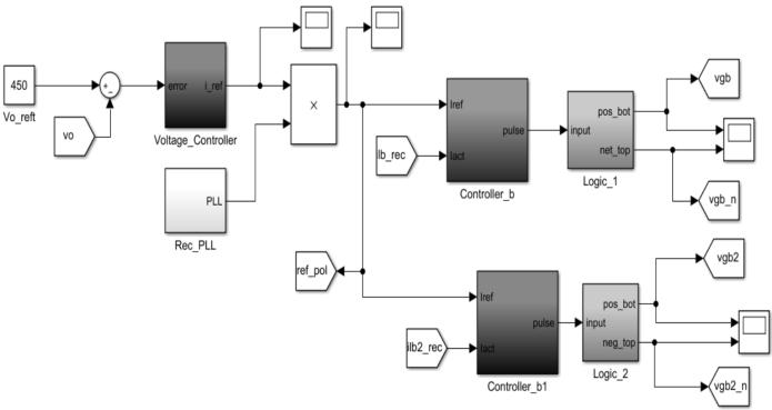
The snapshot of the voltage control loop (at a high level) built-in MATLAB is shown in Fig.9. As seen, the rectified output of the PLL (i.e. rectified unit sine wave), which is in synchronous with the fundamental component of the grid frequency, is multiplied by the peak current reference value, which is generated by the voltage controller block.
4.2 Simulation Results
The results of the simulation circuits presented are included in the following section. The simulation results include the results of the AFC operation in current control mode and voltage control mode.
International Research Journal of Engineering and Technology (IRJET) Volume: 07 Issue: 05 | May 2020 www.irjet.net e-ISSN: 2395-0056 p-ISSN: 2395-0072
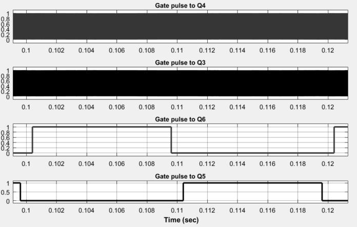
4.2.1 Current Control Mode
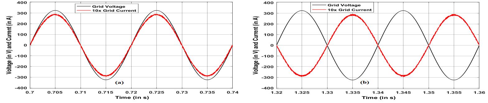
The switching pattern of all the switches G2V mode are shown inFig.10. As seen in these figures, there is a deadtime of around 800 μs between the low-frequency pulses. Fig.10: Switching Pattern of the Switches in AFC Circuit in G2V Mode. values of current references are shown in Fig.11. Fig.11: & in G2V Mode with a Different Values of the Inductor Current. From Fig.10, it is noticed that the grid current follows the reference current with minimum overshoot and settling time. Furthermore, the results in Fig.11 successfully demonstrates the UPF operation. The steady-state waveforms of grid voltage and current (two cycles of grid frequency) during G2V mode at rated condition (i.e. 6.6 kW) is shown in Fig.12. Fig.12: Steady-State Waveforms of the and at Rated Power Conditions During G2V Mode.
The simulations result of the AFC circuit in voltage control mode, where the dc-link voltage regulated by the AFC is as
The grid voltage ( in Black) and scaledup value of the grid current (10xin Red) for different
shown in Fig. 13. Fig.13: Simulation Result Showing dc-link Voltage with a
Reference Value of 450V and Under Load Changing Conditions.
Also, from Fig.13, it is be inferred that voltage ripple in dc-link is limited to below 20V at rated conditions (i.e. at 6.6kW output power).
5. CONCLUSION
The active front-end converter with the aim to charge the electric vehicle battery of 6.6kW is designed. Bridgeless PFC converter is selected that reduces the number of semiconductor switches and also reduces the conduction losses. Totem-pole legs are interleaved so as to increase the overall efficiency and decrease the stress on the switches. The diodes are replaced by the semiconductor switches in order to obtain synchronous rectification. Overall, the converter implemented is totem-pole boost interleaved PFC converter. Converter is designed and simulations results are also shown. Results show the UPF operation of presented converter and the regulatedoutput voltage at the desired value (450 V). The presented converter along with the DC-to-DC converter can be implemented in the design of OBC for EV. And this high efficiency electric vehicle can be used as immediate alternate solution for conventional vehicle.
REFERENCES
[1]
[2] N. Mars, F. Krouz, F. Louar and L. Sbita, "Comparison study of different dynamic battery model," 2017 International Conference on Green Energy Conversion Systems (GECS), Hammamet, 2017, pp. 1-6. doi: 10.1109/GECS.2017.8066241 M. A. Hannan, M. M. Hoque, A. Hussain, Y. Yusof and P. J. Ker, "State-of-the-Art and Energy Management
