International Research Journal of Engineering and Technology (IRJET)
e-ISSN: 2395-0056
Volume: 07 Issue: 02 | Feb 2020
p-ISSN: 2395-0072
www.irjet.net
SILICON BASED MOLECULAR ELECTRONIC Akshat Kumar1, Vishal Jangid2, Abhishek Saxena3 1Student, 2Student,
3Professor,
Dept. of Electronics & Communication, Arya Institute of Engg. & Technology Dept. of Electronics & Communication, Arya Institute of Engg. & Technology
Dept. of Electronics & Communication, Arya Institute of Engg. & Technology College, Jaipur, Rajasthan --------------------------------------------------------------------***-------------------------------------------------------------------Abstract - Molecular electronics on silicon has distinct advantages over its metallic counterpart. We describe a theoretical formalism for transport through semiconductormolecule heterostructures, combining a semi-empirical treatment of the bulk silicon bandstructure with a firstprinciples description of the molecular chemistry and its bonding with silicon. Using this method, we demonstrate that the presence of a semiconducting band-edge can lead to a novel molecular resonant tunneling diode (RTD). 1. INTRODUCTION (RTD) that shows negative differential resistance (NDR) when the molecular levels are driven by an STM potential into the semiconducting band-gap. The peaks appear for positive bias on a pdoped and negative for an n-doped substrate. Charging in these devices is compromised by the RTD action, allowing possible identification of several molecular highest occupied (HOMO) and lowest unoccupied (LUMO) levels. Recent experiments by Hersam et al. [1] support our theoretical predictions.
silicon require a formulation that can account for the bandgap, surface band-bending and surface reconstruction. One problem commonly encountered is that standard quantum chemical basis sets describe molecular energy levels well but provide a very poor description of the semiconductor bandstructure. We present a scheme that can be used to integrate the two distinct systems seamlessly and present results that combine ab initio treatments of the molecule with a semiempirical description of the silicon bands. The same approach can be used to integrate the molecule with more advanced treatments of the silicon substrate. Our results show that we can expect to see NDR using molecules like styrene or TEMPO (2,2’,6,6’-tetramethyl1-piperidynyloxy) on p-silicon at realistic positive sub-
1.1 Theory Traditionally molecular electronic efforts, both theoretical [2, 3] and experimental [4, 5, 6, 7, 8], have been driven by thiol-gold chemistry to molecules bonded to gold substrates. However several recent experiments have demonstrated the feasibility of attaching various molecules on clean silicon surfaces [9]. The development of molecular electronics on silicon is particularly important for two reasons. Firstly, it will enable the development of integrated devices that can utilize the powerful infrastructure provided by the silicon-based IC industry. Secondly, unlike gold, silicon has a bandgap that one can take advantage of to design a new class of resonant tunneling devices with possible applications in logic [10] and low-power memory [11]. In view of these significant potential payoffs we believe it is worthwhile at this time to develop models that can be used to analyze the electrical characteristics of such silicon-based molecular devices. The purpose of this paper is to present (i) a general formulation suitable for modeling silicon-based molecular devices; (ii) realistic principles for designing RTDs based on such structures; and (iii) showing ways to map out the molecular energy spectrum that is not realizable in normal experiments with gold contacts. Molecular devices on
© 2020, IRJET
|
Impact Factor value: 7.34
|
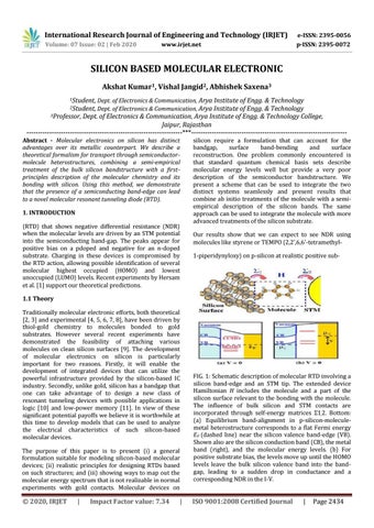
FIG. 1: Schematic description of molecular RTD involving a silicon band-edge and an STM tip. The extended device Hamiltonian H includes the molecule and a part of the silicon surface relevant to the bonding with the molecule. The influence of bulk silicon and STM contacts are incorporated through self-energy matrices Σ1,2. Bottom: (a) Equilibrium band-alignment in p-silicon-moleculemetal heterostructure corresponds to a flat Fermi energy EF (dashed line) near the silicon valence band-edge (VB). Shown also are the silicon conduction band (CB), the metal band (right), and the molecular energy levels. (b) For positive substrate bias, the levels move up until the HOMO levels leave the bulk silicon valence band into the bandgap, leading to a sudden drop in conductance and a corresponding NDR in the I-V.
ISO 9001:2008 Certified Journal
|
Page 2434