International Research Journal of Engineering and Technology (IRJET)
e-ISSN: 2395-0056
Volume: 07 Issue: 01 | Jan 2020
p-ISSN: 2395-0072
www.irjet.net
A Review- FPGA based Architectures for Image Capturing Consequently Processing and Display using VGA Monitor Rohit Raj1, Navneet Singh2 1,2Assistant Professor, Gurdasidevi Institute of Management & Technology, Budhlada- India
---------------------------------------------------------------------***----------------------------------------------------------------------
Abstract - This paper present the accomplishment with
present of image processing submission on field programmable gate array (FPGA). To develop the performance time, Xilinx AccelDSP, software for generate hardware description language (HDL) from a high-level MATLAB description has been used. The designs were implemented on Spartan 3E Starter Board device. Before inscription a processing parts of Image implementation all information regarding data inclusive digital format has been applied. Since we use FPGA as a central part and more give emphasis to on the FPGA, so all the data used in Digital arrangement. A normal nearby boundary, VGA has been broadly old. This controller is industrial using VHDL based in the IEEE standards, to make sure the portability with any user. The structure preserve present whichever illustration. The results illustrate that this anticipated algorithm gives superior performance with diminutive processing time, diminutive power consumption and remembrance usage. Key Words: VGA Controller, VHDL, Image Processing, Xilinx AccelDSP, MATLAB, FPGA, Sparten 3E Starter Board.
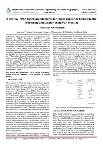
guide to the improvement of electronic system level (ESL) intend and corroboration. The ES design and verification enable embedded system design, authentication, and debug for designing hardware and software implementation of custom system-on-FPGA. The Xilinx AccelDSP instrument is a highly developed ESL drawing tool which transforms a MATLAB floating-point design keen on a hardware module that can be implementing in a Xilinx FPGA. The AccelDSP Synthesis Tool skin tone an easy to use Graphical User Interface (GUI) that wheel an integrated environment with other design tools such as MATLAB, Xilinx ISE tools, and other industry customary HDL simulators and logic synthesizers. This term paper present the devise and execution of FPGA- base structural design for image giving out by employ Xilinx AccelDSP tool. As the Image or any physical data/information always have a flavour of analog, As we are more emphasize on the FPGA as a central part, so all the information/data should be in Digital format. So there we need to convert these information/image/data to digital format.
1. INTRODUCTION The purpose of FPGAs to image processing is a quickly growing research area given recent increase in the power and size of FPGAs. The potential velocity gains make it a smart topic, even though there are many challenges to implement working algorithms on FPGAs. Most new comers consider simply porting an obtainable software algorithm to an FPGA implementation. This project aims to help those wishing to use FPGAs to accelerate image processing algorithms during several of the pitfall, and present a collection of performance to cause in a well-ordered realization, both computationally and in terms of source necessities. Reconfigurable hardware in the figure of Field Programmable Gate Arrays (FPGAs) offers many routine and recital benefits for executing video processing applications. FPGAs normally consist of coherent blocks and some amount of Random Access Memory (RAM/SRAM), all of which are energetic by a huge array of interconnects. All logic in FPGA can be rewired, or reconfigured with different purpose as many times as expensive likes. The advantage of FPGA is its capability to perform operation in corresponding, resulting in remarkable improvement in effectiveness. The foremost gain of FPGA-based proposes be the litheness to acquire improvement of the inherently parallel nature of many image processing problems. The intricacy of generate a aim beginning a set of rations and form increase as the system becomes complex. This difficulty © 2020, IRJET
|
Impact Factor value: 7.34
|
Fig. I: General block diagram on which our effort go.
2. NEED OF FPGA FOR COMPLETION FPGA stands for Field- Programmable Gate Array and an IC that can be programmed following it is manufactured, hence it’s called Field Programmable. Even although the general purpose processors are in receipt of faster every day, image processing applications call for more computational processors, such system can be implement on digital signal processors, it has very expensive Application Specific Integrated Circuits or on FPGA. The plus of FPGA verify by way of the propose of the FPGA conclusion be improved alternative than DSP and ASIC stand on completion. FPGAs are generally programmed
ISO 9001:2008 Certified Journal
|
Page 1643
International Research Journal of Engineering and Technology (IRJET)
e-ISSN: 2395-0056
Volume: 07 Issue: 01 | Jan 2020
p-ISSN: 2395-0072
www.irjet.net
using HDL which uses a low level hardware oriented programming model to fully utilize their potential performance. Although program FPGAs with HDL is moment intense method also additional thorny for great system propose. This circumstance has been changing over with high level programming tools such as Handel-C, AccelDSP and finally Xilinx System Generator for DSP etc. while representation dispensation have for all time been a tough stand toward work scheduled by using FPGA, making this more complicated and interested. The FPGA incorporated giving out structural design exposed in Fig. (II) Consists of four units, initialization unit (INU), and data transfer unit (DTU), image processing unit- IPU and memory management unit- MMU. It manages the entity image to be stored in external memory while the interconnected settings information related to sensor exposure time, frame size, filter selection etc. be store within the domestic remembrance. Initialization part- INU access the basic setting store in the MMU designed for structure initialization when system is ongoing. Image processing unit- IPU does the pipelined operation of the image take into custody, obstacle and understanding.
Fig. II: Block diagram of FPGA incorporated processing Architecture
3. XILINX ACCEL DSP DESIGN FLOW FOR PERFORMANCE ON FPGA The AccelDSP software is the Matlab signal processing model synthesis tool from Xilinx, which allows an algorithm developer to transform a MATLAB floating-point design into a hardware component that can be implemented in silicon. Its most attractive characteristic is that a synthesizable RTL HDL model and a Test bench can be achieved to make certain bit-true, cycle-accurate propose confirmation. The tool also provides script that appeal to and control downstream tools such as HDL simulators, RTL logic synthesizers and implementation tools. Three AccelDSP implementation flows are obtainable as illustrated s h o w n in Fig. (III). The default synthesis flow is called the ISE Synthesis Flow where the main idea is to create an implementation using ISE software and verify the design using HDL gate-level simulation. The next run is call the System Generator flow. In this flow, an IP core is shaped for export and integrates with a larger System Generator design. The third flow, HW Co- Sim, is similar to the ISE flow but the purpose is to simulate the design in hardware platform like a Virtex-4, a Virtex-5, or a Spartan-3E DSP display place. This flood proves to facilitate the design will lope in the object hardware. The AccelDSP IP Core Generators provide a undeviating lane to hardware performance for complex MATLAB built-in and toolbox functions, which when used with the AccelDSP synthesis tool, produces synthesizable and pre-verified intellectual property cores that enables and make easy algorithmic synthesis for Xilinx FPGAs. exposed in the drawing flow diagram Fig. (III) AccelDSP verifies the generated module on each step to be as true as the previous one, or to be personally satisfactory with a small difference during the conversion from floating point design to fixed point. The M-Code mean by and large consists of two parts: a writing and purpose box file. The script files works to generate stimuli, feeds the stimulus to the purpose in a stream loop and verify the output from the function. Moreover, the script file also serves as a source file for future test bench auto invention. AccelDSP firstly analyze the floating-point design to perform the compatibility confirmation of the given MATLAB code to the AccelDSP coding style guidelines. It generates architectures to effort through stream records. The stream reproduction toward create the unlimited flow of records ingoing and parting the suggest is definite in MATLAB with the script-file. It is also important to check that all important variables are observed since the output is used to verify the fixed point model. Subsequently a fixed-point design is achieved. Then the same script file is used to verify the fixed-point design; by compare it with the saved output outcome of the golden model, to make certain the correctness of the design. If the results are unproductive, the user has to go back and interpret the design with more directions or to control or change the floating-point design. This iteration is performed until the user is fulfilled with the results.
© 2020, IRJET
|
Impact Factor value: 7.34
|
ISO 9001:2008 Certified Journal
|
Page 1644
International Research Journal of Engineering and Technology (IRJET)
e-ISSN: 2395-0056
Volume: 07 Issue: 01 | Jan 2020
p-ISSN: 2395-0072
www.irjet.net
The after that step is to generate an RTL design and a test bench at the same time. Model Sim or other simulation tools are used to simulate the generated RTL design, which compares the test bench output with the saved fixed-point simulation output. The verification passes if all values are the same. This design flow genuinely speeds up the conversion process from a MATLAB model to a RTL hardware version.
4. INITIALIZATION UNIT (INU) When the initialization unit receives the initiate signal, addresses are generating to MMU, instructions in MMU are sent to Initialization unit. The instructions are decoded to generate different signals to the related units for necessary initial settings.
Fig. IV: Block chart of Initialization part.
5. IMAGE PROCESSING UNIT (IPU)
Fig. V: Building block systematize and data links of IPU It shows the sort out and data relations of Image Processing Unit to supplementary unit while bright as to the inside part. Picture dealing out Unit contain three parts to be strict:1. 2. 3.
image capture 2-D convolve 2-D sorters.
Fig. III: Since scheme necessity and algorithm growth to Xilinx AccelDSP synthesis design flow option implements.
© 2020, IRJET
|
Impact Factor value: 7.34
|
ISO 9001:2008 Certified Journal
|
Page 1645
International Research Journal of Engineering and Technology (IRJET)
e-ISSN: 2395-0056
Volume: 07 Issue: 01 | Jan 2020
p-ISSN: 2395-0072
www.irjet.net
6. Memory administration Unit and Data transmit Unit The remaining two units, Memory Management Unit (MMU) and Data transfer Unit (DTU) are describing at this end. MMU consists of two module, restriction module and image module. Parameter component include an internal memory for storing the parameter initialization settings. Image module takes care of the entity image storing from IPU or the state formally form external memory to PC through Data Transfer Unit (DTU). The associates stuck between MMU, DTU, PC, INU, IPU and external memory shown in Fig.(VI).
7.1 VGA Edge Port VGA boundary sends equivalent display signals to display through DB-15 linker which is directly connected to Monitor or LCD by monitor cable. There are 15 pinholes which are irregularly separated into 3 lines, and there are 5 on each line.
Fig. VII: VGA interface port
7.2 VGA Monitor Organizer Arch.
Fig. VI: Correlation among MMU, DTU, INU and IPU
7. VGA MONITOR VGA (Video Graphics array) as a typical interface has already been applications extensively. There are a lot of FPGA-based VGA controller designs on which, though there are still larger defects such as low-resolution display and display modules occupy large resource. The design of resourceful hardware architecture for VGA Monitor using VHDL as a logical means to describe the completion of highresolution VGA control module and a resource -conserving twine present unit devise, and give two major module of scheming thought moreover common sense diagram. It ensures a high-resolution display, the storage resources needed by the display decreased extensively. Such a design can in actual fact solve the problems cause by inadequate bandwidth in the display what more it can diminish the strain of the CPU.VGA (video graphics array) is a video display standard. It provides a simple method to connect a system with a monitor for presentation information or images. As a standard display interface, VGA has been broadly used. Present is more and more need in displaying the result of the process in real time as the fast growth of embedded system, particularly the expansion of high speed image processing.
© 2020, IRJET
|
Impact Factor value: 7.34
|
Fig. VIII: VGA observe manager architecture. Here are two clock domains in this aim: system clock and pixel clock. The system clock is the source clock for the side of bus interface while the pixel clock is worn for the side of VGA interface. The pixel clock frequency is necessary according to the display customary. It can be ambitious by an on-chip clock generator or an off-chip clock generator.
8. CONCLUSIONS Here I’ll make an effort to do the same concept by using completely from HDLs i.e. VHDL and its implementation through FPGA by greatest using EDA Tool(s) Electronic design automation i.e. Xilinx ISE. As FPGAs are reconfigurable this can be utilize in Real time Embedded Systems for protection, computerization etc. By with FPGAs as a innermost unit the designer may not be accepted to review the various structural designs of processor based systems for a same set of problem. The same design can be taken for ASIC flow and the chip can be
ISO 9001:2008 Certified Journal
|
Page 1646
International Research Journal of Engineering and Technology (IRJET)
e-ISSN: 2395-0056
Volume: 07 Issue: 01 | Jan 2020
p-ISSN: 2395-0072
www.irjet.net
Mass- Manufactured to construct the chip to the market at lower cost and higher profit. In this we have existing wellorganized hardware architecture for VGA monitor controller which has a high potential to be used. The adorned characteristic, make the design suitable and capable to meet different necessities of besieged application. At the equivalent time together image and text personality display at the same time. Special of use at all resulting RAM memory. Simply by means of On Chip embedded array memory it displays the facial outer shell of communally image and character display in the screen.
REFERENCES [1] Said, Yahia, Taoufik Saidani, and Mohamed Atri. "FPGA-based architectures for image processing using high-level design." WSEAS Trans. Signal Process 11 (2015): 38-44. [2] Deepika, K., M. Jabeen, and K. Sridivya. "Implementation of image processing algorithms using xilinx system generator." J Innov Electron Commun Eng 5.1 (2015): 24-29. [3] Chang, Chi-Jeng, Pei-Yung Hsiao, and Zen-Yi Huang. "Integrated operation of image capturing and processing in FPGA." IJCSNS International Journal of Computer Science and Network Security 6.1A (2006): 173-179. [4] Gonzales, Rafael C., and Richard E. Woods. "Digital image processing." (2002). [5] Crookes, D., et al. "Design and implementation of a high level programming environment for FPGA-based image processing." IEE Proceedings-Vision, Image and Signal Processing 147.4 (2000): 377-384.
[10] Crookes, D., et al. "Design and implementation of a high level programming environment for FPGA- based image processing." IEE Proceedings-Vision, Image and Signal Processing 147.4 (2000): 377-384. [11] Lakshminarayanan, G., et al. "Design and implementation of FPGA based wavepipelined fast convolver." 2000 TENCON Proceedings. Intelligent Systems and Technologies for the New Millennium (Cat. No. 00CH37119). Vol. 3. IEEE, 2000. [12] Benkrid, Khaled, Danny Crookes, and Abdsamad Benkrid. "Towards a general framework for FPGA based image processing using hardware skeletons." Parallel Computing 28.7-8 (2002): 1141-1154. [13] Bouridane, Ahmed, et al. "A high level FPGA-based abstract machine for image processing." Journal of systems architecture 45.10 (1999):809-824. [14] Taright, Yamina, and Michel Hubin. "FPGA implementation of a multilayer perceptron neural network using VHDL." ICSP'98. 1998 Fourth International Conference on Signal Processing (Cat. No. 98TH8344). Vol. 2. IEEE, 1998. [15] Raj, Rohit, Monika Aggarwal, and Gaurav Mittal. "Review on HDL Implementation of Digital Image Display on VGA." International Journal of Computer Applications 975: 8887. [16] Zhu, Yi-Dan, and Yi-Bing Fang. "Image acquisition and VGA display system based on FPGA [J]." Journal of Computer Applications 5.9 (2011): 1258-1261.
[6] Hiraiwa, Jorge, Enrique Vargas, and Sergio Toral. "An FPGA based embedded vision system for real-time motion segmentation." Proceedings of 17th International Conference on Systems, Signals and Image Processing. Brazil. 2010. [7] Wasu, Renuka A., and Vijay R. Wadhankar. "Design and Implementation of VGA Controller on FPGA." International Journal of Innovative Research in Computer and Communication Engineering 3.7 (2015). [8] Chiuchisan, Iuliana. "A new FPGA-based real-time configurable system for medical image processing." 2013 E-Health and Bioengineering Conference (EHB). IEEE, 2013. [9] Gawhane, Dhiraj R., et al. "Design and Implementation of a Digital Image Processor for Image Enhancement Techniques using Verilog Hardware Description Language." International Journal of Computer Technology and Applications 5.1 (2014): 87. © 2020, IRJET
|
Impact Factor value: 7.34
|
ISO 9001:2008 Certified Journal
|
Page 1647