International Research Journal of Engineering and Technology (IRJET)
e-ISSN: 2395-0056
Volume: 06 Issue: 05 | May 2019
p-ISSN: 2395-0072
www.irjet.net
Design and Simulation of Comparator Architectures for Various ADC Applications Disha Gaude1, Bathini Poornima2, K. M. Sudharshan3, Prashant V. Joshi4 1,2,3,4Dept.
of Electronics and communication Engineering, REVA University, Bengaluru, India ----------------------------------------------------------------------***---------------------------------------------------------------------
Abstract - This paper presents design and simulation of different CMOS comparators. The designs are simulated and studied in 180 nm Technology with Cadence Virtuoso Tool with supply voltage 3.3 V and reference voltage of 3V. The clock used in comparator has a frequency of 1 M Hz. The comparators are mostly used in converting analog signals to digital signals for processing. Comparators are used in the applications requiring less power dissipation, good accuracy and high resolution.
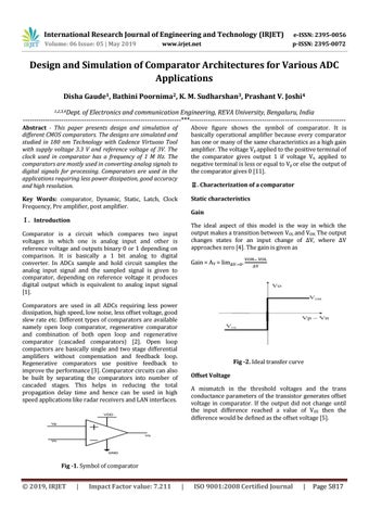
Above figure shows the symbol of comparator. It is basically operational amplifier because every comparator has one or many of the same characteristics as a high gain amplifier. The voltage Vp applied to the positive terminal of the comparator gives output 1 if voltage Vn applied to negative terminal is less or equal to Vp or else the output of the comparator gives 0 [11].
Key Words: comparator, Dynamic, Static, Latch, Clock Frequency, Pre amplifier, post amplifier.
Static characteristics
Ⅱ. Characterization of a comparator
Gain
Ⅰ. Introduction
The ideal aspect of this model is the way in which the output makes a transition between VOL and VOH. The output changes states for an input change of ΔV, where ΔV approaches zero [4]. The gain is given as
Comparator is a circuit which compares two input voltages in which one is analog input and other is reference voltage and outputs binary 0 or 1 depending on comparison. It is basically a 1 bit analog to digital converter. In ADCs sample and hold circuit samples the analog input signal and the sampled signal is given to comparator, depending on reference voltage it produces digital output which is equivalent to analog input signal [1].
Gain = AV =
Comparators are used in all ADCs requiring less power dissipation, high speed, low noise, less offset voltage, good slew rate etc. Different types of comparators are available namely open loop comparator, regenerative comparator and combination of both open loop and regenerative comparator (cascaded comparators) [2]. Open loop compactors are basically single and two stage differential amplifiers without compensation and feedback loop. Regenerative comparators use positive feedback to improve the performance [3]. Comparator circuits can also be built by separating the comparators into number of cascaded stages. This helps in reducing the total propagation delay time and hence can be used in high speed applications like radar receivers and LAN interfaces.
Fig -2. Ideal transfer curve Offset Voltage A mismatch in the threshold voltages and the trans conductance parameters of the transistor generates offset voltage in comparator. If the output did not change until the input difference reached a value of V OS then the difference would be defined as the offset voltage [5].
Fig -1. Symbol of comparator
© 2019, IRJET
|
Impact Factor value: 7.211
|
ISO 9001:2008 Certified Journal
|
Page 5817