International Research Journal of Engineering and Technology (IRJET)
e-ISSN: 2395-0056
Volume: 06 Issue: 05 | May 2019
p-ISSN: 2395-0072
www.irjet.net
Impact of Buffer Mole Fraction on AlGaN/ GaN HEMT with Different Gate Voltage Abdul Shekkeer KM1, Taru Doni2, Ravisankar Varma K3, Shalom Frandev3 1,2,3,4Dept.of
Basic and Applied Science, National Institute of Technology Arunachal Pradesh, India ---------------------------------------------------------------------***---------------------------------------------------------------------
Abstract - The effect of buffer mole fraction on AlGaN/GaN field plated High Electron Mobility Transistor (HEMT) with
composite AlGaN/GaN buffer were investigated. The sandwich of AlGaN and GaN mainly depends on Al mole fraction as it defines the band gap and lattice constant of AlGaN. Increasing mole fraction will results in increased drain current. This can be explained by the fact that the increasing mole fraction leads to higher polarization. The analytical relation between 2DEG density and the barrier potential (at the AlN/GaN interface) and other parameters in the HEMT is summarizing by the equations (1 & 2). And with the help of silvaco software we simulate and show the output of I-V curve of drain current vs drain voltage and source current vs drain voltage. Key Words: HEMT, AlGaN, GaN, 2DEG, Mole fraction
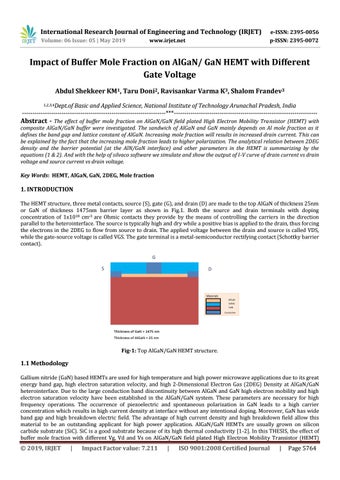
1. INTRODUCTION The HEMT structure, three metal contacts, source (S), gate (G), and drain (D) are made to the top AlGaN of thickness 25nm or GaN of thickness 1475nm barrier layer as shown in Fig.1. Both the source and drain terminals with doping concentration of 1x1018 cm-3 are Ohmic contacts they provide by the means of controlling the carriers in the direction parallel to the heterointerface. The source is typically high and dry while a positive bias is applied to the drain, thus forcing the electrons in the 2DEG to flow from source to drain. The applied voltage between the drain and source is called VDS, while the gate-source voltage is called VGS. The gate terminal is a metal-semiconductor rectifying contact (Schottky barrier contact).
Fig-1: Top AlGaN/GaN HEMT structure.
1.1 Methodology Gallium nitride (GaN) based HEMTs are used for high temperature and high power microwave applications due to its great energy band gap, high electron saturation velocity, and high 2-Dimensional Electron Gas (2DEG) Density at AlGaN/GaN heterointerface. Due to the large conduction band discontinuity between AlGaN and GaN high electron mobility and high electron saturation velocity have been established in the AlGaN/GaN system. These parameters are necessary for high frequency operations. The occurrence of piezoelectric and spontaneous polarization in GaN leads to a high carrier concentration which results in high current density at interface without any intentional doping. Moreover, GaN has wide band gap and high breakdown electric field. The advantage of high current density and high breakdown field allow this material to be an outstanding applicant for high power application. AlGaN/GaN HEMTs are usually grown on silicon carbide substrate (SiC). SiC is a good substrate because of its high thermal conductivity [1-2]. In this THESIS, the effect of buffer mole fraction with different Vg, Vd and Vs on AlGaN/GaN field plated High Electron Mobility Transistor (HEMT)
Š 2019, IRJET
|
Impact Factor value: 7.211
|
ISO 9001:2008 Certified Journal
|
Page 5764