International Research Journal of Engineering and Technology (IRJET)
e-ISSN: 2395-0056
Volume: 06 Issue: 05 | May 2019
p-ISSN: 2395-0072
www.irjet.net
RELIABILITY ENHANCEMENT OF LOW-POWER SEQUENTIAL CIRCUITS USING POWER GATING TECHNOLOGY Deepa Jose1, Juby Raju2, Saju A3 1PG
Scholar, Dept of ECE, MCET, Kerala professor, Dept of ECE, MCET, Kerala 3Research Scholar, VTU, Karnataka ---------------------------------------------------------------------***--------------------------------------------------------------------2Associate
Abstract – This paper deals with low-power ASIC designs with power gating technology. They compromises with high performance and low area and power consumption, taking advantage of both latch and flip-flop features. While the circuit reliability and robustness against different process, voltage, and temperature variations are considered as critical issues with current technologies, no significant reliability study was proposed for traditional transmission gate pulsed latch circuits. In this paper, present a study on the effect of different PVT variations on the behavior traditional transmission gate pulsed latch circuits with power gating technology , while keeping their main advantages of high performance, low power, and small area. The proposed designs have negligible power overhead when running at nominal supply voltage, and they have higher yield per unit power when compared with the traditional design at different voltages and temperatures. The proposed circuit is implemented using Tanner v13 in 45 nm technology.
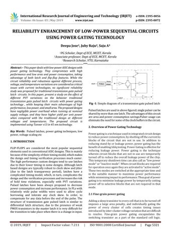
Fig -1: Simple diagram of a transmission gate pulsed latch Pulsed latches are used in above figured; single pulser can be shared by more than one latch. The advantages of this circuit are area and power consumption savings.Pulser usage can eliminate the need for some of the clock buffers in the circuit. 2. Overview of Power Gating Technology
Key Words: Pulsed latches, power gating techniques, low power, voltage scaling etc
Power gating is a technique used in integrated circuit design to reduce power consumption, by shutting off the current to blocks of the circuit that are not in use. In addition to reducing stand-by or leakage power, power gating has the benefit of enabling Iddq testing. Power Gating is effective for reducing leakage power. Power gating is the technique wherein circuit blocks that are not in use are temporarily turned off to reduce the overall leakage power of the chip. This temporary shutdown time can also call as "low power mode" or "inactive mode". When circuit blocks are required for operation once again they are activated to "active mode". These two modes are switched at the appropriate time and in the suitable manner to maximize power performance while minimizing impact to performance. Thus goal of power gating is to minimize leakage power by temporarily cutting power off to selective blocks that are not required in that mode.
1. INTRODUCTION FLIP-FLOPS are considered the most popular sequential elements used in conventional ASIC designs. This is mainly because of the simplicity of their timing model, which makes the design and timing verification processes much easier. The high performance custom designs tend to use latches due to their lower timing in some designs. Although latch based designs are typically robust to clock skew and jitter (due to the latch transparency period), latches have a complicated timing model, which, in turn, complicates the design and the verification processes and increases the risk of hold time violations, especially with PVT variations. Pulsed latches have been always proposed to decrease power consumption and increase performance. In PLs with relatively wide pulse widths were used to allow cycle borrowing and tolerate any clock skew. In order, to compensate for any data before the end of the pulse. The structure of transmission gate pulsed latch is similar to differential latch structure, due to the presence of weak PMOS transistors in the master latch it is very difficult for the transition to take place when there is a change in input.
Š 2019, IRJET
|
Impact Factor value: 7.211
2.1 Fine-grain power gating Adding a sleep transistor to every cell that is to be turned off imposes a large area penalty, and individually gating the power of every cluster of cells creates timing issues introduced by inter-cluster voltage variation that are difficult to resolve. Fine-grain power gating encapsulates the switching transistor as a part of the standard cell logic.
|
ISO 9001:2008 Certified Journal
|
Page 5321