International Research Journal of Engineering and Technology (IRJET)
e-ISSN: 2395-0056
Volume: 06 Issue: 03 | Mar 2019
p-ISSN: 2395-0072
www.irjet.net
Design of an Inductive Source Degenarative Low Noise Amplifier using 180nm CMOS Technology M. Kiran Kumar1, Amrita Sajja2, Katti Blessy Beulah3 ,K. Sree Deepthi 4, Ravalika D5 1,2Assistant
Professor, Dept. of ECE Anurag Group Of Institutions,Hyderabad scholar & Anurag Group Of Institutions, Hyderabad
3,4,5Research
---------------------------------------------------------------------***--------------------------------------------------------------------Abstract - In this paper attributes a design of cascaded narrowband low noise amplifier (LNA) operated at 2.4GHz using inductive source degeneration with a shunt connected inductor and resistance transformer matching. This design implementing with CMOS transistor from gpdk180nm technology. By introducing inductive source degeneration will degrade the gain while improving the stability and maintaining the noise figure of the overall system. With shunt connected transformer provides narrow band characteristic and good input and output return loss on the desired frequency band. The LNA achieves input and output return loss of less than -20 dB, gain 25dB and noise figure less than 0.6dB respectively.
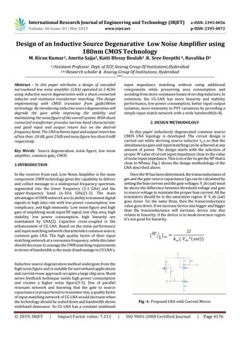
input impedance matching without using additional components while preserving area consumption and avoiding from more resistance losses of on-chip inductors. In extension, the CG-LNA has more linearity and stability performance, low power consumption, better input-output isolation, more immunity to PVT variations by providing a simple input match network with a wide bandwidth[6-8]. 2. DESIGN METHODOLOGY In this paper inductively degenerated common source CMOS LNA topology is developed. The circuit design is carried out while deriving source inductor L_s so that the simultaneous gain and input matching can be achieved at any amount of power. The design starts with the selection of proper W value of circuit input impedance close to the value of noise input impedance. This is in order to get the NF that is close to NFmin. Fig.1 shows the design methodology of the LNA described above.
Key Words: Source degeneration, noise figure, low noise amplifier, common gate, CMOS 1.INTRODUCTION In the receiver front end, Low Noise Amplifier is the main component. UWB technology gives the capability to deliver and collect message in a widespread frequency spectrum, segmented into the lower frequency (3-5 GHz) and the upper-frequency band (6-10.6 GHz)[1-3]. The main advantages of UWB network are its ability to transmit digital signals in high data rate with low power consumption, low complicacy, and high immunity. Low noise figure and high gain of amplifying weak input RF signal, low chip area, high stability, low power consumption, high linearity are maintained by LNA[2]. Capacitor cross-coupled is the enhancement of CG LNA. Based on the noise performance and input matching network characteristics common source, common gate LNA. The high quality factor of their input matching network at a resonance frequency, while this later should decrease to assuage the UWB matching requirements in terms of bandwidth is the main disadvantage in CS LNA's.
Once the W has been determined, the transconductance of gm and the gate-source capacitance Cgs can be calculated by setting the bias current and the gate voltages. V_ds (sat) must be above the difference between threshold voltage and gate to source voltage to maintain the proper bias current. All the transistors should be in the saturation region. If V_ds (sat) goes down for the same Ibias; then the transconductance value goes down. If we increase device size bigger and bigger than the transonductance will increase; device size also relates to linearity; if the device is in weak inversion region it’s not good for linearity.
Inductive source degeneration method undergoes from the high noise figure and is suitable for narrowband applications and current reuse approach occupies a large chip area. Shunt series feedback technique needs high power consumption and creates a higher noise figure[3-5]. Due of parallel resonant network and knowing that the gate to source capacitance is proportional to transistor size, a quality factor of input matching network of CG LNA would decrease when the technology should be scaled down and bandwidth shows wideband demeanor. So CG LNA has a constant wideband
Š 2019, IRJET
|
Impact Factor value: 7.211
Fig -1: Proposed LNA with Current Mirror
|
ISO 9001:2008 Certified Journal
|
Page 4176